NSC CX9210-VNG Datasheet
© 2000 National Semiconductor Corporation www.national.com
Geode™ CS9210 Graphics Companion DSTN Controller
April 2000
Geode™ CS9210 Graphics Companion
DSTN Controller
General Description
The CS9210 graphics companion is suitable for systems
that use either the GXLV or GXm processor along with the
CS5530 I/O companion; all members of the National
Semiconductor
®
Geode™ family of products. The
CS9210 converts the digital RGB output streamto thedigital graphics input stream required by most industry standard DSTN color flat panel LCDs. It can drive all standard
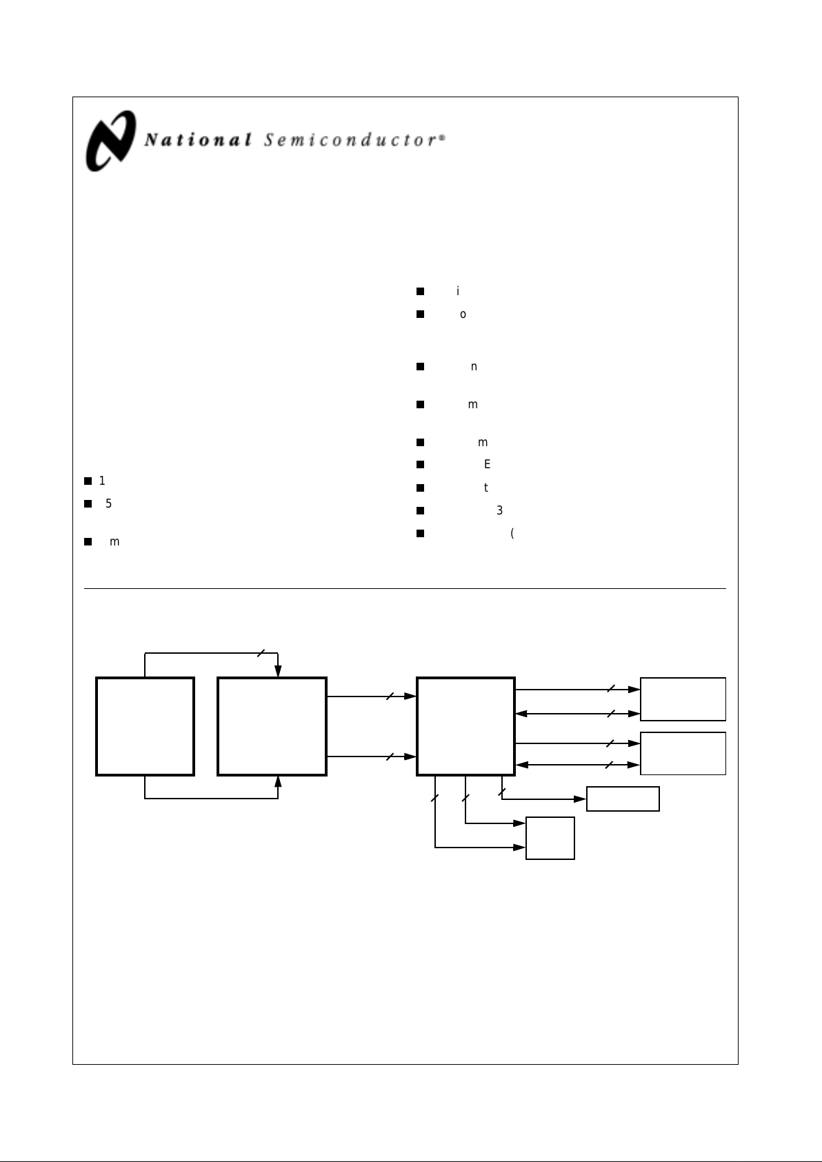
DSTN flat panels up to a 1024x768 resolution. The system connection example shows how the CS9210 interfaces with the rest of the system components.
Features
18-bit color support for digital pixel input
65 MHz pixel clock operation supports up to 1024x768
panels
SimultaneousCRTand DSTN display with up to 75 Hz
refresh rate
2X display refresh modes, up to 120 Hz
Supports most SVGA DSTN panels and the VESA
FPDI (Flat Panel Display Interface) Revision 1.0
Specification
TFT panel support provided by use of one connector;
allows a pass-through mode for the digital pixel input
Programmableframe rate modulation (FRM), up to 32
levels
Programmabledither, up to 16 levels
Supports EDO memory, 16-bit interface
Configuration via a serial programming interface
Low-power, 3.3V operation
144-pin LQFP (Low-profile Quad Flat Pack)
Geode™ CS9210 System Connection Example
DRAM Data
Addr Control
13
16
LCD Power
3
Control
Clocks
316
Panel Data
DSTN
PixelPort
24
PixelData
LCD
18
Geode™
GXm
Geode™
Geode™
CS9210
Graphics
CS5530
DRAM-B
256Kx16 bit
or
GXLV
Processor
DRAM-A
256Kx16 bit
Addr Control
13
DRAM Data
16
4
Serial
Configuration
I/O
Companion
Companion
Video Port (YUV)
National Semiconductor is a registered trademark of National Semiconductor Corporation.
Geode is a trademark of National Semiconductor Corporation.
For a complete listing of National Semiconductor trademarks, please visit www.national.com/trademarks.

www.national.com 2 Revision 3.2
Table of Contents
Geode™ CS9210
1.0 ArchitectureOverview..............................................3
2.0 SignalDefinitions..................................................4
2.1 PINASSIGNMENTS .......................................................4
2.2 SIGNALDESCRIPTIONS ...................................................8
2.2.1 PixelPortInterfaceSignals ...........................................8
2.2.2 SerialInterfaceSignals ..............................................9
2.2.3 FlatPanelInterfaceSignals ...........................................9
2.2.4 MemoryInterfaceSignals ...........................................10
2.2.5 ResetandInternalTestPins .........................................11
2.2.6 PowerandGroundPins .............................................11
3.0 Functional Description . . . . . . . . . . . . . . . . . . . . . . . . . . . . . . . . . . . . . . . . . . . . 12
3.1 MODESELECTION .......................................................12
3.2 2XREFRESHMODE ......................................................14
3.3 TIMINGSIGNALSANDPANELCLOCK .......................................15
3.4 SIMULTANEOUSDISPLAY .................................................15
3.5 MAXIMUMFREQUENCY...................................................16
3.6 RESET PROCEDURES . . . . . . . . ............................................16
3.7 SERIALINTERFACE ......................................................16
3.8 COLORGENERATION ....................................................18
3.8.1 FrameRateModulation(FRM)........................................18
3.8.1.1 ChoosingFRMSequences ..........................................18
3.8.1.2 RemovalofFlickering ..............................................20
3.8.2 Dithering.........................................................20
3.8.2.1 N-BitDitheringSchemes ............................................21
3.8.3 CombiningFRMandDithering........................................22
3.8.3.1 ModifiedFRMandDithering .........................................22
3.9 PROGRAMMINGTHEFRMANDDITHERMEMORIES...........................22
3.9.1 AddressingtheFRMMemories .......................................22
3.9.2 AddressingtheDitheringMemories....................................23
4.0 RegisterDescriptions .............................................24
5.0 ElectricalSpecifications ...........................................30
5.1 ABSOLUTEMAXIMUMRATINGS............................................30
5.2 RECOMMENDEDOPERATINGCONDITIONS..................................30
5.3 DCCHARACTERISTICS ..................................................31
5.4 ACCHARACTERISTICS ...................................................32
5.4.1 PixelPortTiming ..................................................33
5.4.2 SerialInterfaceTiming ..............................................34
5.4.3 FlatPanelTiming ..................................................35
5.4.4 MemoryInterfaceTiming ...........................................36
6.0 MechanicalPackageOutline .......................................37
Appendix A Support Documentation . . . . . . . . . . . . . . . . . . . . . . . . . . . . . . . . . . . . 38
A.1 REVISIONHISTORY ......................................................38
Revision 3.2 3 www.national.com
Geode™ CS9210
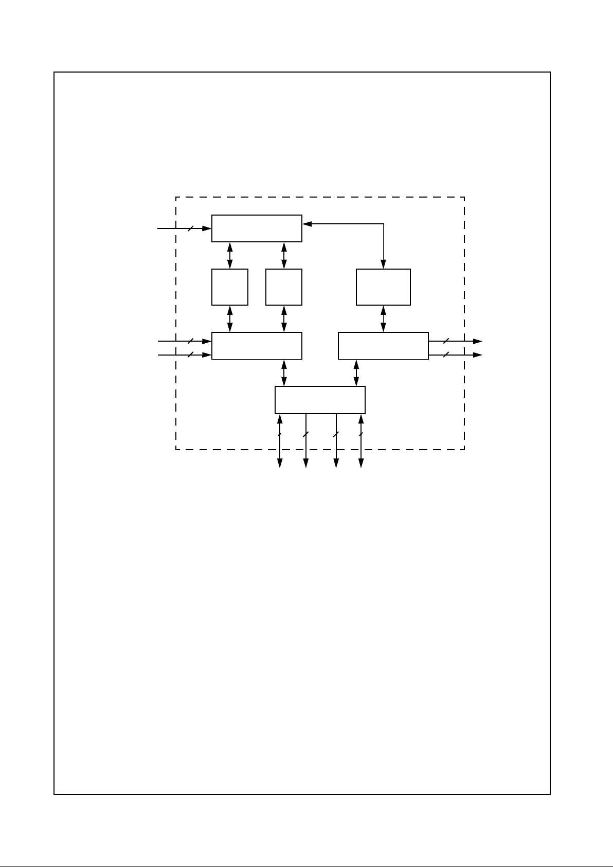
1.0 Architecture Overview
The major functional blocks, as shown in Figure 1-1, of
the Geode CS9210 graphics companion:
• Serial Interface
• DitherMemory
• FRM Memory
• Control Registers
• DSTN Formatter
• Display Controller
• DRAM Controller
Figure 1-1. Internal Block Diagram
Serial Interface
DSTN Formatter
Dither
Memory
FRM
Memory
Control
Registers
Display Controller
DRAM Controller
Pixel Control
6
Pixel Data
18
Serial Configuration
4
Panel Control
Panel Data
6
16
13 13
DRAM
Bank A
DRAM
Bank B
16 16
DRAM Data
DRAM Data
Addr Ctrl
Addr Ctrl
www.national.com 4 Revision 3.2
Geode™ CS9210
2.0 Signal Definitions
This section defines the signals and external interface of
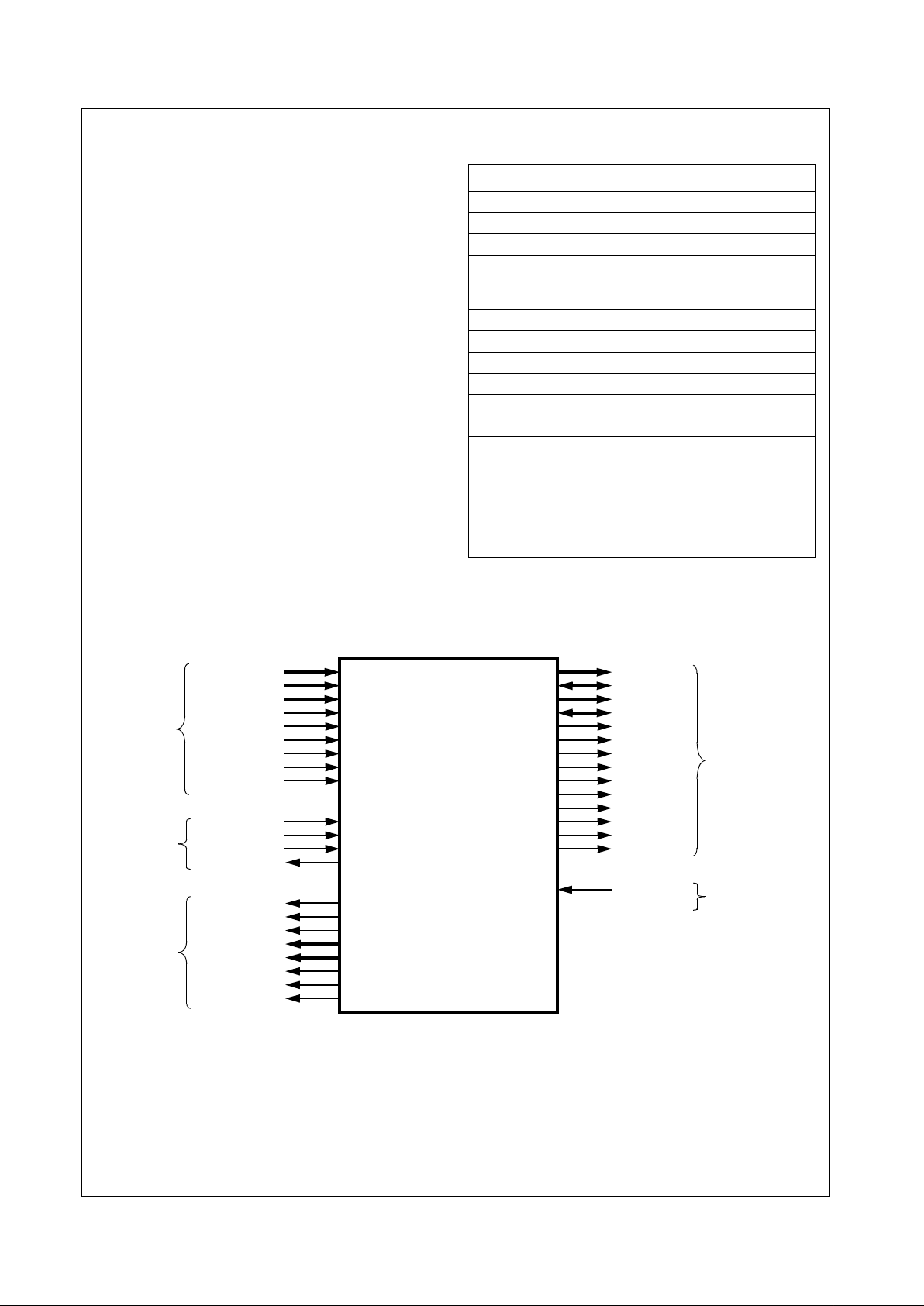
the Geode CS9210. Figure 2-1 shows the pins organized
by their functional groupings (internal test and electrical
pins are not shown).
2.1 PIN ASSIGNMENTS
The tables in this section use several common abbreviations. Table 2-1 lists the mnemonics and their meanings.
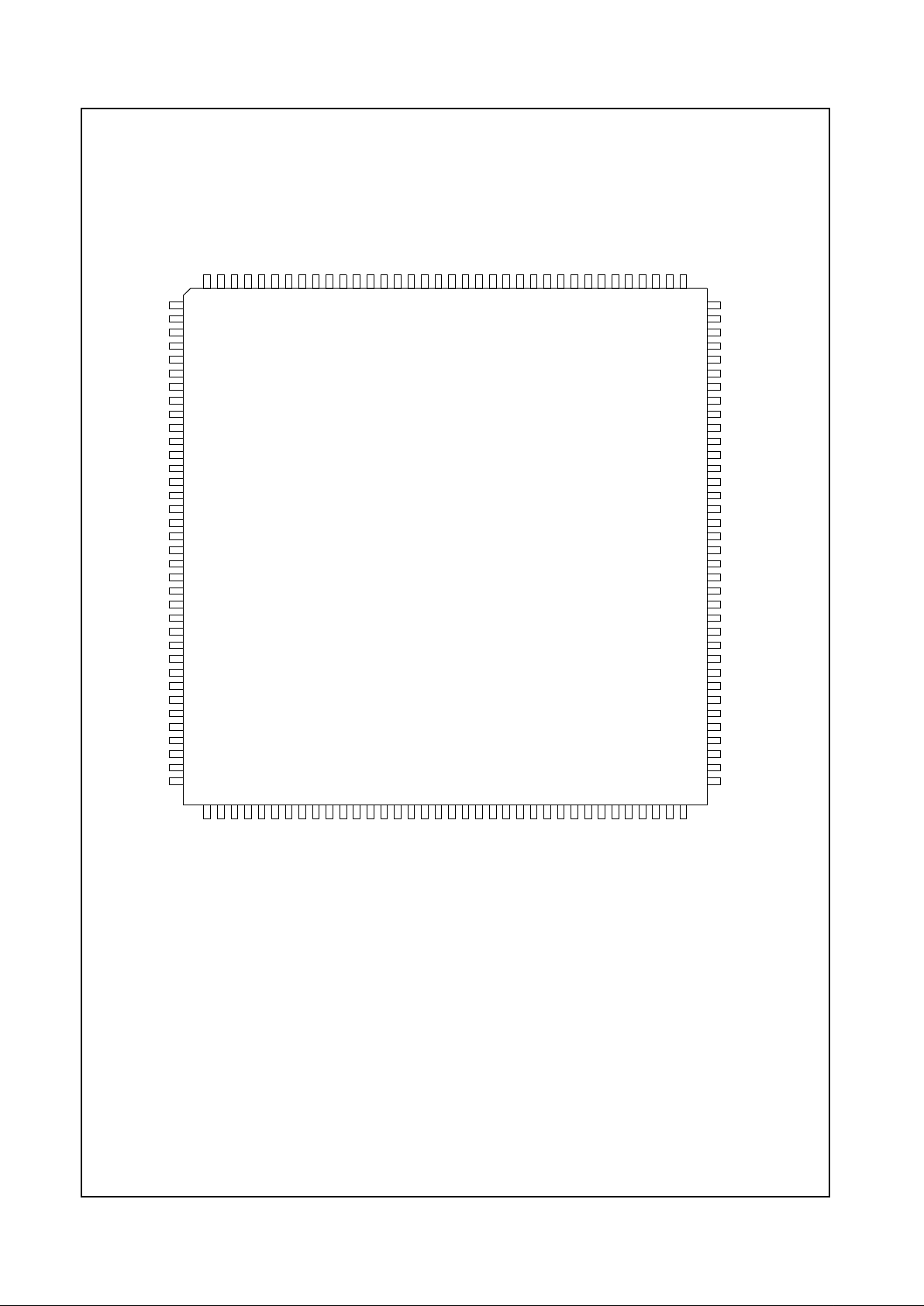
Figure 2-2 shows the pin assignment for the CS9210 with
Tables 2-2 and 2-3 listing the pin assignments sorted by
pin number and alphabetically by signal name, respectively.
In Section 2.2 “Signal Descriptions” a description of each
signal within its associated functional group is provided.
Figure 2-1. CS9210 S ignal Groups
Table 2-1. Pin Type Definitions
Mnemonic Definition
I Standard input pin.
I/O Bidirectional pin.
O Totem-pole output.
OD Open-drain output structure that
allows multiple devices to share the
pin in a wired-OR configuration
PU Pull-up resistor
PD Pull-down resistor
smt Schmitt Trigger
t/s Tri-state signal
VDD (PWR) Power pin.
VSS (GND) Ground pin
# The "#" symbol at the end of a signal
name indicates that the active or
asserted state occurswhen the signal
is at a lowvoltage level.When "#" is
not present after the signal name, the
signal is asserted when at a highvolt-
age level.
RED[5:0]
GREEN[5:0]
BLUE[5:0]
ENA_DISP
ENA_VDDIN
ENA_LCDIN
DOTCLK
FP_HSYNC
FP_VSYNC
SCLK
SDIN
SCS
SDO
LP
SHFCLK
FLM
UD[11:0]
LD[11:0]
DISPOFF#
FP_VDDEN
FP_VCONEN
MA_A[9:0]
MD_A[15:0]
MA_B[9:0]
MD_B[15:0]
OEA#
OEB#
RASA#
RASB#
LCASA#
UCASA#
LCASB#
UCASB#
RESET#
Memory
Interface
Reset
Interface
Flat Panel
Interface
Pixel Port
Interface
Geode™ CS9210
Graphics
Serial
Interface
WEA#
WEB#
Companion
Revision 3.2 5 www.national.com
Signal Definitions (Continued)
Geode™ CS9210
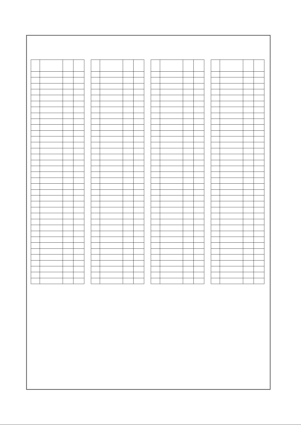
Figure 2-2. 144-Pin LQFP Pin A ssignment Diagram
Order Number: CS9210-VNG
1
2
3
4
5
6
7
8
9
10
11
12
13
14
15
16
17
18
19
20
21
22
23
24
25
26
27
28
29
30
31
32
33
34
35
36
3738394041424344454647484950515253545556575859606162636465666768697071
72
108
107
106
105
104
103
102
101
100
99
98
97
96
95
94
93
92
91
90
89
88
87
86
85
84
83
82
81
80
79
78
77
76
75
74
73
144
143
142
141
140
139
138
137
136
135
134
133
132
131
130
129
128
127
126
125
124
123
122
121
120
119
118
117
116
115
114
113
112
111
110
109
Geode™ CS9210
Graphics Companion
VDD
VSS
FP_HSYNC
GREEN1
GREEN2
GREEN3
GREEN4
GREEN5
RED0
RED1
RED2
RED3
RED4
RED5
SCLK
SDIN
VDD
VSS
VSS
DOTCLK
SCS
SDO
MA_A9
MA_A8
MA_A7
MA_A6
MA_A5
MA_A4
MA_A3
MA_A2
MA_A1
MA_A0
MD_A15
MD_A14
MD_A13
VDD
VDD
VSS
MD_B6
MD_B5
MD_B4
MD_B3
MD_B2
MD_B1
MD_B0
OEB#
UCASB#
LCASB#
RASB#
WEA#
RASA#
LCASA#
VDD
VSS
OEA#
UCASA#
MD_A0
MD_A1
MD_A2
MD_A3
MD_A4
MD_A5
MD_A6
MD_A7
MD_A8
MD_A9
MD_A10
MD_A11
MD_A12
VSS
VDD
VDD
LD11
LD10
LD9
LD8
LD7
LD6
LD5
LD4
LD3
LD2
LD1
LD0
MA_B9
MA_B8
MA_B7
MA_B6
VDD
VSS
VSS
MA_B5
MA_B4
MA_B3
MA_B2
MA_B1
MA_B0
MD_B15
MD_B14
MD_B13
MD_B12
MD_B11
MD_B10
MD_B9
MD_B8
MD_B7
VDD
VSS
SHFCLK
UD0
UD1
UD2
UD3
UD4
UD5
UD6
UD7
UD8
UD9
UD10
UD11
FLM
TEST
VDD
VSS
LP
VSS
FP_VCONEN
FP_VDDEN
DISPOFF#
RESET#
ENA_LCDIN
ENA_VDDIN
ENA_DISP
BLUE0
BLUE1
BLUE2
BLUE3
BLUE4
BLUE5
GREEN0
FP_VSYNC
VDD
WEB#
Top View
www.national.com 6 Revision 3.2
Signal Definitions (Continued)
Geode™ CS9210
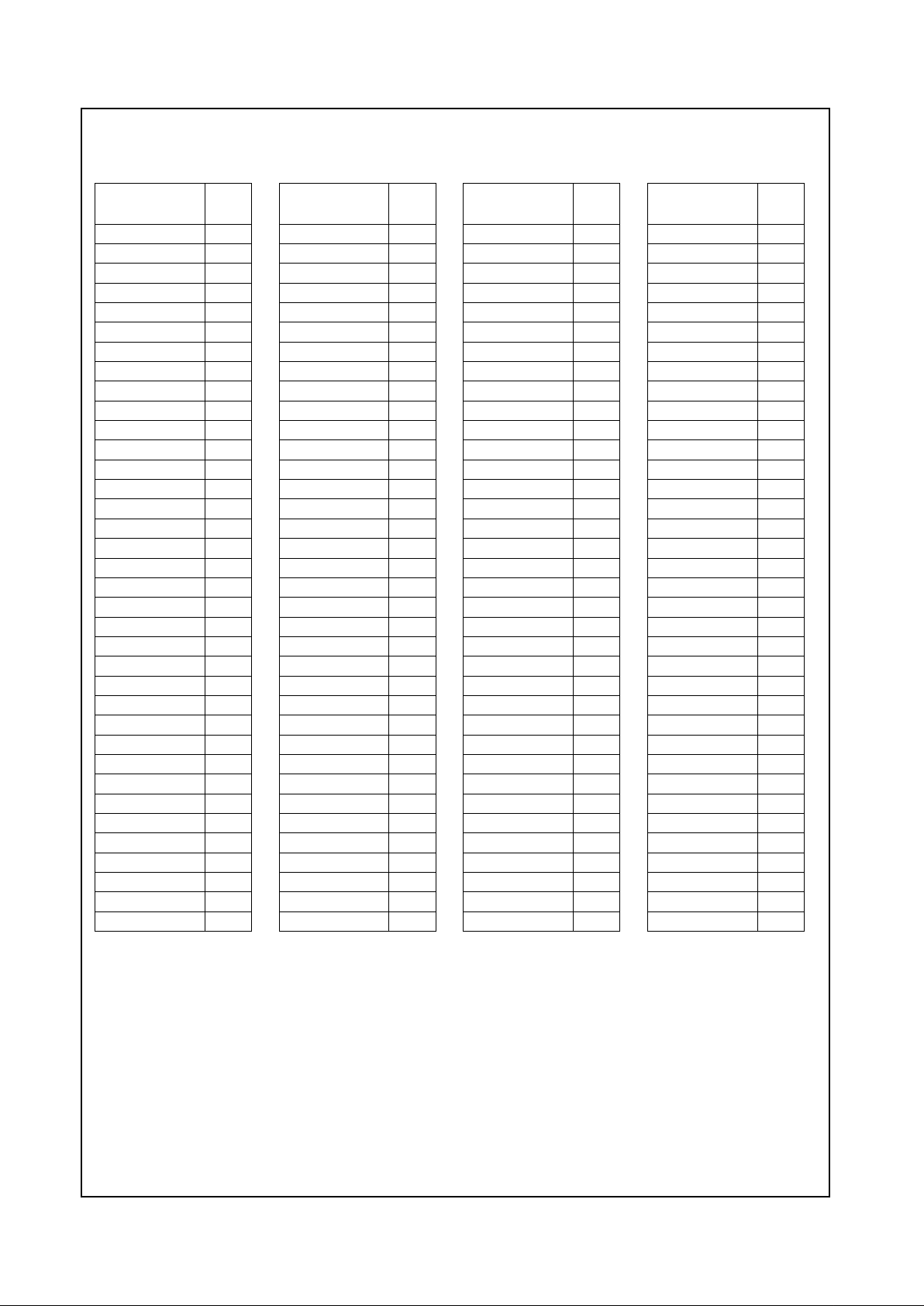
Table 2-2. Pin Assignments - Sorted by P in Number
Pin
No. Signal Name Type
Drive
(mA)
1VDD PWR -2 VSS GND -3 F P_HSYNC I -4GREEN1 I -5GREEN2 I -6GREEN3 I -7GREEN4 I -8GREEN5 I --
9RED0 I -10 RED1 I -11 RED2 I -12 RED3 I -13 RED4 I -14 RED5 I -15 SCLK I -16 SDIN I -17 VDD PWR -18 VSS GND -19 VSS GND -20 DOTCLK I -21 SCS I -22 SDO O 6
23 MA_A9 O 4
24 MA_A8 O 4
25 MA_A7 O 4
26 MA_A6 O 4
27 MA_A5 O 4
28 MA_A4 O 4
29 MA_A3 O 4
30 MA_A2 O 4
31 MA_A1 O 4
32 MA_A0 O 4
33 MD_A15 I/O 4
34 MD_A14 I/O 4
35 MD_A13 I/O 4
36 VDD PWR --
37 VDD PWR -38 VSS GND -39 MD_A12 I/O 4
40 MD_A11 I/O 4
41 MD_A10 I/O 4
42 MD_A9 I/O 4
43 MD_A8 I/O 4
44 MD_A7 I/O 4
45 MD_A6 I/O 4
46 MD_A5 I/O 4
47 MD_A4 I/O 4
48 MD_A3 I/O 4
49 MD_A2 I/O 4
50 MD_A1 I/O 4
51 MD_A0 I/O 4
52 UCASA# O 4
53 OEA# O 4
54 VSS GND -55 VDD PWR -56 LCASA# O 4
57 RASA# O 4
58 WEA# O 4
59 WEB# O 4
60 RASB# O 4
61 LCASB# O 4
62 UCASB# O 4
63 OEB# O 4
64 MD_B0 I/O 4
65 MD_B1 I/O 4
66 MD_B2 I/O 4
67 MD_B3 I/O 4
68 MD_B4 I/O 4
69 MD_B5 I/O 4
70 MD_B6 I/O 4
71 VSS GND -72 VDD PWR --
Pin
No. Signal Name Type
Drive
(mA)
73 VDD PWR -74 MD_B7 I/O 4
75 MD_B8 I/O 4
76 MD_B9 I/O 4
77 MD_B10 I/O 4
78 MD_B11 I/O 4
79 MD_B12 I/O 4
80 MD_B13 I/O 4
81 MD_B14 I/O 4
82 MD_B15 I/O 4
83 MA_B0 O 4
84 MA_B1 O 4
85 MA_B2 O 4
86 MA_B3 O 4
87 MA_B4 O 4
88 MA_B5 O 4
89 VSS GND -90 VSS GND -91 VDD PWR -92 MA_B6 O 4
93 MA_B7 O 4
94 MA_B8 O 4
95 MA_B9 O 4
96 LD0 O 12
97 LD1 O 12
98 LD2 O 12
99 LD3 O 12
100 LD4 O 12
101 LD5 O 12
102 LD6 O 12
103 LD7 O 12
104 LD8 O 12
105 LD9 O 12
106 LD10 O 12
107 LD11 O 12
108 VDD PWR --
Pin
No. Signal Name Type
Drive
(mA)
109 VSS GND -110 SHFCLK O 12
111 UD0 O 12
112 UD1 O 12
113 UD2 O 12
114 UD3 O 12
115 UD4 O 12
116 UD5 O 12
117 UD6 O 12
118 UD7 O 12
119 UD8 O 12
120 UD9 O 12
121 UD10 O 12
122 UD11 O 12
123 FLM O 12
124 TEST I -125 VDD PWR -126 VSS GND -127 LP O 12
128 VSS GND -129 FP_VCONEN O 12
130 FP_VDDEN O 1 2
131 DISPOFF# O 12
132 RESET# I -133 ENA_LCDIN I -134 ENA_VDDIN I -135 ENA_DISP I -136 BLUE0 I -137 BLUE1 I -138 BLUE2 I -139 BLUE3 I -140 BLUE4 I -141 BLUE5 I -142 GREEN0 I -143 FP_VSYNC I -144 VDD PWR --
Pin
No. Signal Name Type
Drive
(mA)
Revision 3.2 7 www.national.com
Signal Definitions (Continued)
Geode™ CS9210
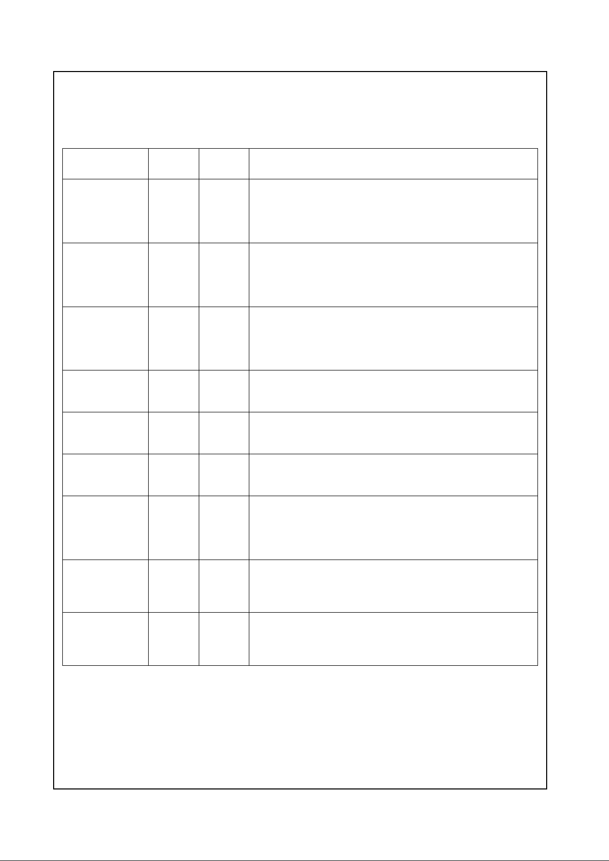
Table 2-3. Pin Assignments - Sorted Alphabetically by Signal Name
Signal Name
Pin
No.
BLUE0
136
BLUE1 137
BLUE2 138
BLUE3 139
BLUE4 140
BLUE5 141
DISPOFF# 131
DOTCLK 20
ENA_DISP 135
ENA_LCDIN 133
ENA_VDDIN 134
FLM 123
FP_HSYNC 3
FP_VCONEN 129
FP_VDDEN 130
FP_VSYNC 143
GREEN0 142
GREEN1 4
GREEN2 5
GREEN3 6
GREEN4 7
GREEN5 8
LCASA# 56
LCASB# 61
LD0 96
LD1 97
LD10 106
LD11 107
LD2 98
LD3 99
LD4 100
LD5 101
LD6 102
LD7 103
LD8 104
LD9 105
LP 127
MA_A0 32
MA_A1 31
MA_A2 30
MA_A3 29
MA_A4 28
MA_A5 27
MA_A6 26
MA_A7 25
MA_A8 24
MA_A9 23
MA_B0 83
MA_B1 84
MA_B2 85
MA_B3 86
MA_B4 87
MA_B5 88
MA_B6 92
MA_B7 93
MA_B8 94
MA_B9 95
MD_A0 51
MD_A1 50
MD_A2 49
MD_A3 48
MD_A4 47
MD_A5 46
MD_A6 45
MD_A7 44
MD_A8 43
MD_A9 42
MD_A10 41
MD_A11 40
MD_A12 39
MD_A13 35
MD_A14 34
Signal Name
Pin
No.
MD_A15 33
MD_B0 64
MD_B1 65
MD_B2 66
MD_B3 67
MD_B4 68
MD_B5 69
MD_B6 70
MD_B7 74
MD_B8 75
MD_B9 76
MD_B10 77
MD_B11 78
MD_B12 79
MD_B13 80
MD_B14 81
MD_B15 82
OEA# 53
OEB# 63
RASA# 57
RASB# 60
RED0 9
RED1 10
RED2 11
RED3 12
RED4 13
RED5 14
RESET# 132
SCLK 15
SCS 21
SDIN 16
SDO 22
SHFCLK 110
TEST 124
UCASA# 52
UCASB# 62
Signal Name
Pin
No.
UD0 111
UD1 112
UD2 113
UD3 114
UD4 115
UD5 116
UD6 117
UD7 118
UD8 119
UD9 120
UD10 121
UD11 122
VDD 1
VDD 17
VDD 36
VDD 37
VDD 55
VDD 72
VDD 73
VDD 91
VDD 108
VDD 125
VDD 144
VSS 2
VSS 18
VSS 19
VSS 38
VSS 54
VSS 71
VSS 89
VSS 90
VSS 109
VSS 126
VSS 128
WEA# 58
WEB# 59
Signal Name
Pin
No.
www.national.com 8 Revision 3.2
Signal Definitions (Continued)
Geode™ CS9210
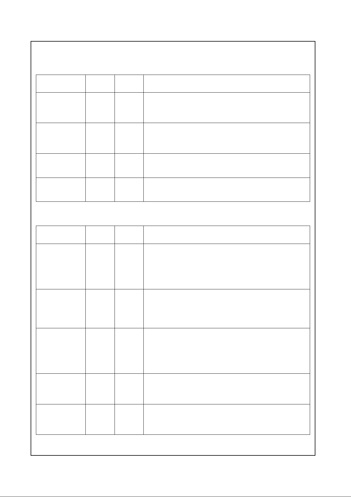
2.2 SIGNAL DESCRIPTIONS
2.2.1 Pixel Port Interface Signals
Signal Name Pin No.
Type
(Drive) Description
RED[5:0] 14-9 I Red Pixel Channel
These six pins are the red component of the pixel port input. The six
most significant bits of the CS5530 pixel port (FP_DATA[17:12] on an
18-bit pixel port) are connected to these pins. RED5 is the MSB (most
significant bit) and RED0 is the LSB (least significant bit).
GREEN[5:0] 8-4,142 I Green Pixel Channel
These six pins are the green component of the pixelport input. The six
middle bits of the CS5530 pixel port (FP_DATA[11:6] on an 18-bit pixel
port) are connected to these pins. GREEN5 is theMSB and GREEN0
is the LSB.
BLUE[5:0] 141-136 I Blue Pixel Channel
These six pins are the bluecomponent of the pixel port input. The six
least significant bits of the CS5530 pixel port (FP_DATA[5:0]on an 18bit pixel port) are connected to these pins. BLUE5 is the MSB and
BLUE0 is the LSB.
ENA_DISP 135 I Active Display Enable
This input is asserted when the pixel data stream is presenting valid
displaydata to the pixel port.
ENA_VDDIN 134 I Input VDD Enable
When this input is asserted, it indicates that the display controller in
the CS9210 should apply voltage to the LCD panel.
ENA_LCDIN 133 I Input LCD Enable
When this input is asserted, it indicates that the display controller in
the CS9210 should drive valid control signals to the LCD panel.
DOTCLK 20 I Dot Clock
This signal is the pixel clock from thevideo controller. It is used to
clock data in from thepixel port. Additionally, this signal is used as the
inputclock forthe entire CS9210device.This clock must be running at
all times after reset for the CS9210 to function correctly.
FP_HSYNC 3 I Flat Panel Horizontal Sync Input
When the input data stream is in a horizontal blanking period, this
input is asserted. It is a pulse that isused to synchronize displaylines
and to indicate when the pixel data stream is not valid due to blanking.
FP_VSYNC 143 I Flat Panel Vertical Sync Input
When the input data stream is in a vertical blanking period, this inputis
asserted. It is a pulse used to synchronize display frames and toindicate when the pixel data stream is not valid due to blanking.
Revision 3.2 9 www.national.com
Signal Definitions (Continued)
Geode™ CS9210
2.2.2 Serial Interface Signals
Signal Name Pin No.
Type
(Drive) Description
SCLK 15 I Serial Interface Clock
This input signal is the clock for the serial controlinterface. The other
serial interface signals (SDIN, SCS, SDO) are synchronous to this signal.
SDIN 16 I Serial Data Input
This is the data input line for the serial control interface. Input data is
serializedon this pin, including the commandstream forregister reads
and writes.
SDO 22 O
(6 mA)
Serial Data Output
This is the data output line for the serial control interface. Output data
is serialized on this pin in response to register read commands.
SCS 21 I Serial Chip Select
This active high chipselect indicates when valid data is being clocked
in or out via the SDIN/SDO pins.
2.2.3 Flat Panel Interface Signals
Signal Name Pin No.
Type
(Drive) Description
LP 127 O
(12 mA)
Latch Pulse
This is the line pulseor latch pulsefor the flat panel data,indicating
the output data is notvalid, a display line has endedand another is
about to start.
Depending on the type of panel beinginterfaced, this signal can also
be referred to as CL1 or LINE.
SHFCLK 110 O
(12 mA)
Panel Clock (Shift Clock)
This is the shift clock or pixelclock for the flat panel data. This signal is
used to clock pixel data into the LCD panel.
Depending on the type of panel beinginterfaced, this signal can also
be referred to as CL2 or SHIFT.
FLM 123 O
(12 mA)
First Line Marker
This is the frame pulse for the flat panel data indicating the output data
is not valid, and one display frame has ended and another is about to
start.
Depending on the type of panel beinginterfaced, this signal can also
be referred to as FP or FRAME.
UD[11:0] 122-111 O
(12 mA)
Upper Scan Data
These outputs are the upper panel pixel data bus to the DSTN LCD
panel. Its format is dependent on thedisplay mode configured for the
LCD panel. Refer to Section 3.1 “ModeSelection” on page 12.
LD[11:0] 107-96 O
(12 mA)
Lower Scan Data
These outputs are the lower panel pixel data bus to the DSTN LCD
panel. Its format is dependent on thedisplay mode configured for the
LCD panel. Refer to Section 3.1 “ModeSelection” on page 12.
www.national.com 10 Revision 3.2
Signal Definitions (Continued)
Geode™ CS9210
DISPOFF# 131 O
(12 mA)
Disables Panel
When this output is asserted low, it indicates that the LCD panel
should be disabled.
FP_VDDEN 130 O
(12 mA)
Controls LCD VDD FET
When this output is asserted high, voltage should be applied to the
panel. This signal is intended to controla power FET to the LCD
panel.
FP_VCONEN 129 O
(12 mA)
Controls LCD Bias Voltage Enable
When this output is asserted high, the contrast voltage(VCON) should
be applied to the panel.
2.2.3 Flat Panel Interface Signals (Continued)
Signal Name Pin No.
Type
(Drive) Description
2.2.4 Memory Interface Signals
Signal Name Pin No.
Type
(Drive) Description
MA_A[9:0] 23-32 O
(4 mA)
DRAM Bank A Address Bus
The address bus for Bank A of the DRAM.
MD_A[15:0] 33-35,
39-51
I/O
(4 mA)
DRAM Bank A Data Bus
The data bus for Bank A of the DRAM.
MA_B[9:0] 95-92,
88-83
O
(4 mA)
DRAM Bank B Address Bus
The address bus for Bank B of the DRAM.
MD_B[15:0] 82-74,
70-64
I/O
(4 mA)
DRAM Bank B Data Bus
The data bus for Bank B of the DRAM.
OEA# 53 O
(4 mA)
DRAM Bank A Output Enable
The output enable for Bank A of the DRAM.
OEB# 63 O
(4 mA)
DRAM Bank B Output Enable
The output enable for Bank B of the DRAM.
RASA# 57 O
(4 mA)
DRAM Bank A Row Address Strobe
The row address strobe for Bank A of the DRAM.
RASB# 60 O
(4 mA)
DRAM Bank B Row Address Strobe
The row address strobe for Bank B of the DRAM.
UCASA# 52 O
(4 mA)
DRAM Bank A High Byte Column Address Strobe
The column address strobe for the upper eight bits of data for Bank A
of the DRAM.
LCASA# 56 O
(4 mA)
DRAM Bank A Low Byte Column Address Strobe
The column address strobe for the lower eight bits of data for Bank A
of the DRAM.
UCASB# 62 O
(4 mA)
DRAM Bank B High Byte Column Address Strobe
The column address strobe for the upper eight bits of data for Bank B
of the DRAM.

Revision 3.2 11 www.national.com
Signal Definitions (Continued)
Geode™ CS9210
LCASB# 61 O
(4 mA)
DRAM Bank B Low Byte Column Address Strobe
The column address strobe for the lower eight bits of data for Bank B
of the DRAM.
WEA# 58 O
(4 mA)
DRAM Bank A Write Enable
The write enable signal for Bank A of the DRAM.
WEB# 59 O
(4 mA)
DRAM Bank B Write Enable
The write enable signal for Bank B of the DRAM.
2.2.4 Memory Interface Signals (Continued)
Signal Name Pin No.
Type
(Drive) Description
2.2.5 Reset and Internal Test Pins
Signal Name Pin No.
Type
(Drive) Description
RESET# 132 I Reset
This pin is the system reset input.
TEST 124 I Reserved
This pin must be tied to ground. It is a National Semiconductor internal
test mode pin only.
2.2.6 Power and Ground Pins
Signal Name Pin No.
Type
(Drive) Description
VDD 1, 17, 36,
37, 55,
72, 73,
91, 108,
125, 144
PWR Power Connection (total of 11 pins)
Power for the DRAM and system interface signals. These should be
supplied with 3.3V.
VSS 2, 18, 19,
38, 54,
71, 89,
90, 109,
126, 128
GND Ground Connection (total of 11 pins)
Ground connection.
www.national.com 12 Revision 3.2
Geode™ CS9210
3.0 Functional Description
The Geode CS9210 graphics companion connects to the
TFT port of the CS5530 I/O companion chip (see Figure
3-1). It formats the graphics refresh data for the DSTN display and controls the refresh of the DSTNLCD.
The CS9210 must be connected to two 60ns EDO
(Extended Data Out) 256Kx16 DRAMs that store a DSTNformatted copy of the frame buffer. Pixel data is received
by the pixel port, formatted by a programmable FRM
(Frame Rate Modulator) and dither block, and then stored
in the CS9210 frame buffer. The formatted pixel data is
subsequently read from the DRAMs and used to refresh
the DSTN panel. The panel can be refreshed at 1X or 2X
the input refresh rate, up to a maximum refresh rate of
120Hz.UsingtwobanksofDRAM,theCS9210controls
each bank independently to allow for maximal use of the
DRAM bandwidth and to minimize the amount of on-chip
buffering.
The FRM/dithering formatting is accomplished via a pair
of mapping RAMs. The first is used for FRM coloring; the
second for dithering. The FRM RAM is a 32x64-bit map,
representing 64 frames of data for 32 color patterns. The
dithering RAM is a 16x4x4-bit map, yielding 16 dithering
levels. The RAM-based FRM/dither approach gives the
OEM the most flexibility to tune the FRM and dithering
algorithms for a specificpanel.
The FRM and dither maps are loaded, along with the
remaining control registers, through a simple serial programming port that connects to the CS5530 I/O companionchipasillustratedinFigure3-1.Figure3-2showsan
alternative connection method.
3.1 MODE SELECTION
The CS9210 can be configured for three modes of operation. The mode selected depends on the type of panel
being connected to the flat panelinterface:
• 16-bit DSTN Mode
- Supports DSTN panels with 640x480or 800x600
resolutions.
• 24-bit DSTN Mode
- Supports DSTN panels with 1024x768 pixel resolution.
• TFT Pass-Through Mode
- Allows a common connector to be used for TFT LCD
panels and DSTN LCD panels.The system software
can configure the CS9210 to operate in a PassThrough mode that presents the digitalpixel (RGB)
input data on the UD/LD output pins to drive a TFT
panel on the common connector. The input data is
registered internally before being presented at the
output pins to better c ontrol the timing of the panel
interface signals.
Mode selection is programmed via Index 02h, bits 1 and 0
as shown in Table 3-1. Depending on the mode selected,
the panel data that is presented on the UD/LD buses will
vary.
Figure 3-1. CS5530 and CS9210 Signal Connections
GPIOx
GPIOx
GPIOx
GPIOx
FP_ENA_VDD
FP_DISP_ENA_OUT
FP_CLK
FP_HSYNC
FP_VSYNC
FP_DATA[5:0]
FP_DATA[11:6]
FP_DATA[17:12]
SCLK
SDIN
SCS
SDO
ENA_LCDIN
ENA_VDDIN
ENA_DISP
DOTCLK
FP_HSYNC
FP_VSYNC
BLUE[5:0]
GREEN[5:0]
RED[5:0]
Geode™
VCC3
Geode™
CS5530 I/O
CS9210
Companion
Graphics
Companion
 Loading...