

NSC CLC5622IN, CLC5622IMX, CLC5622IM Datasheet
Features
■
130mA output current
■
0.05%, 0.03° differential gain, phase
■
3.0mA/ch supply current
■
160MHz bandwidth (Av= +2)
■
-90/-97dBc HD2/HD3 (1MHz)
■
18ns settling to 0.05%
■
370V/µs slew rate
■
Stable for capacitive loads up to 1000pf
■
Single 5V or ±5V supplies
Applications
■
Video line driver
■
ADSL/HDSL driver
■
Coaxial cable driver
■
UTP differential line driver
■
Transformer/coil driver
■
High capacitive load driver
■
Portable/battery-powered applications
■
Differential A/D driver
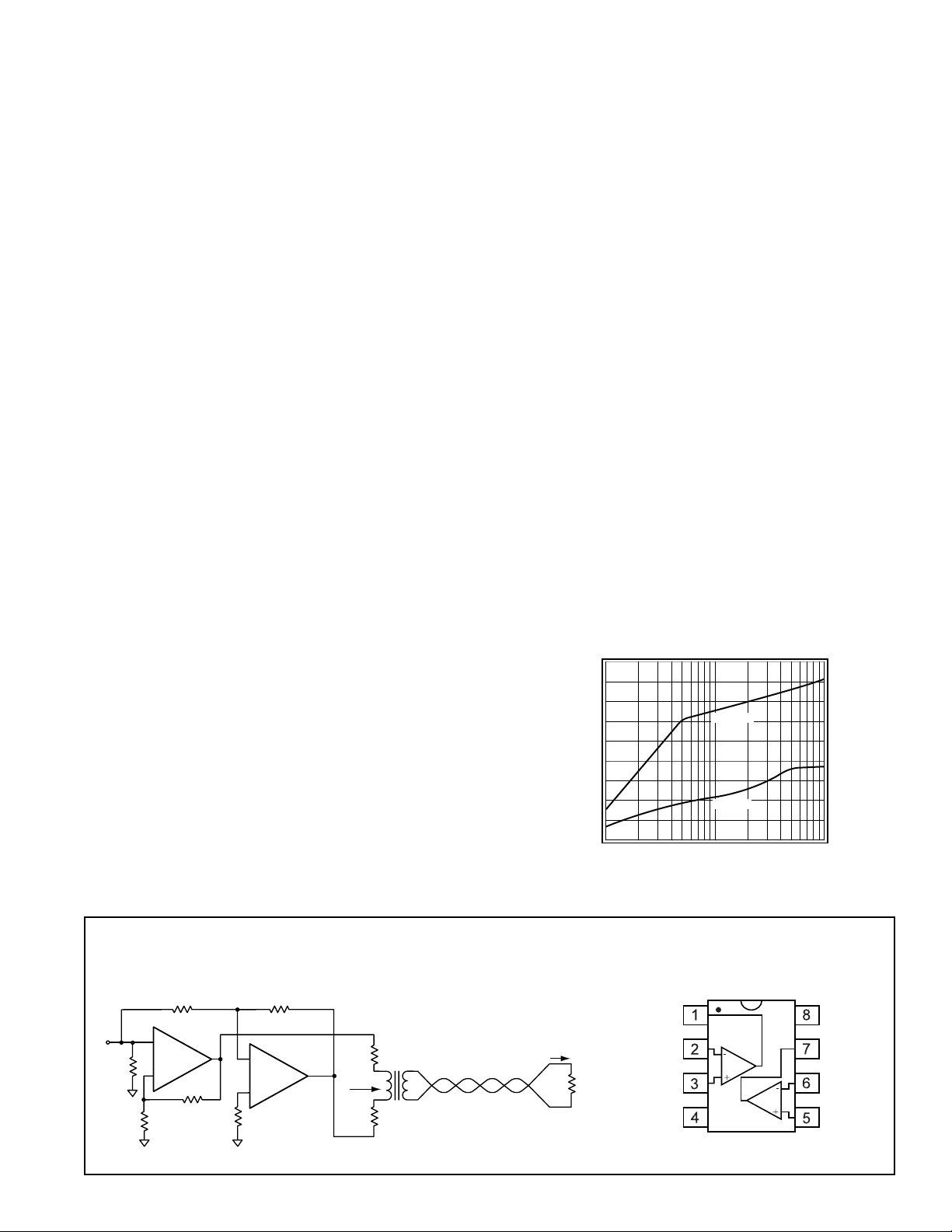
Typical Application
Differential Line Driver with Load Impedance Conversion
Pinout
DIP & SOIC
General Description
The National CLC5622 has a new output stage that delivers high
output drive current (130mA), but consumes minimal
quiescent supply current (3.0mA/ch) from a single 5V supply. Its
current feedback architecture, fabricated in an advanced complementary bipolar process, maintains consistent performance over
a wide range of gains and signal levels, and has a linear-phase
response up to one half of the -3dB frequency.
The CLC5622 offers 0.1dB gain flatness to 30MHz and differential gain and phase errors of 0.05% and 0.03°. These features are
ideal for professional and consumer video applications.
The CLC5622 offers superior dynamic performance with a
160MHz small-signal bandwidth, 370V/µs slew rate and 4.4ns
rise/fall times (2V
step
). The combination of low quiescent power,
high output current drive, and high-speed performance make
the CLC5622 well suited for many battery-powered personal
communication/computing systems.
The ability to drive low-impedance, highly capacitive loads,
makes the CLC5622 ideal for single ended cable applications.
It also drives low impedance loads with minimum distortion.
The CLC5622 will drive a 100Ω load with only -95/-95dBc
second/third harmonic distortion (Av= +2, V
out
= 2Vpp, f = 1MHz).
With a 25Ω load, and the same conditions, it produces only -72/
-77dBc second/third harmonic distortion.
The CLC5622 can also be used for driving differential-input step-
up transformers for applications such as Asynchronous Digital
Subscriber Lines (ADSL) or High-Bit-Rate Digital Subscriber
Lines (HDSL).
When driving the input of high-resolution A/D converters, the
CLC5622 provides excellent -90/-97dBc second/third harmonic
distortion (Av= +2, V
out
= 2Vpp, f = 1MHz, RL= 1kΩ) and fast
settling time.
CLC5622
Dual, High Output,Video Amplifier
N
June 1999
CLC5622
Dual, High Output, Video Amplifier
© 1999 National Semiconductor Corporation http://www.national.com
Printed in the U.S.A.
Maximum Output Voltage vs. R
10
9
)
8
pp
7
6
5
4
3
Output Voltage (V
2
1
10
VCC = ±5V
Vs = +5V
100
RL (Ω)
L
1000
R
g2
V
V
in
+
CLC5622
R
t1
-
R
g1
d/2
1/2
R
f1
R
t2
R
-
1/2
CLC5622
+
f2
Vo1
V
1
V
non-inv
-V
inv
1
CC
-V
d/2
R
m/2
1:n
R
eq
R
m/2
Z
UTP
o
I
o
+
R
V
L
o
-
+V
Vo2
V
inv
V
non-inv
CC
2
2
http://www.national.com 2
PARAMETERS CONDITIONS TYP MIN/MAX RATINGS UNITS NOTES
Ambient Temperature CLC5622IN/IM +25°C +25°C 0 to 70°C -40 to 85°C
FREQUENCY DOMAIN RESPONSE
-3dB bandwidth V
o
= 0.5V
pp
130 100 90 85 MHz
V
o
= 2.0V
pp
95 80 77 75 MHz
-
0.1dB bandwidth Vo= 0.5V
pp
30 25 20 20 MHz
gain peaking <200MHz, V
o
= 0.5V
pp
0 0.5 0.9 1.3 dB
gain rolloff <30MHz, V
o
= 0.5V
pp
0.1 0.4 0.6 0.6 dB
linear phase deviation <30MHz, V
o
= 0.5V
pp
0.15 0.3 0.4 0.4 deg
differential gain NTSC, R
L
= 150Ω to -1V 0.03 – – – %
differential phase NTSC, R
L
= 150Ω to -1V 0.07 – – – deg
TIME DOMAIN RESPONSE
rise and fall time 2V step 4.5 6.0 6.4 6.8 ns
settling time to 0.05% 1V step 17 25 40 60 ns
overshoot 2V step 11 15 18 18 %
slew rate 2V step 280 195 165 150 V/µs
DISTORTION AND NOISE RESPONSE
2
nd
harmonic distortion 2Vpp, 1MHz -79 -76 -73 -73 dBc
2V
pp
, 1MHz; RL= 1kΩ -80 -78 -75 -75 dBc
2V
pp
, 5MHz -66 -60 -58 -58 dBc
3
rd
harmonic distortion 2Vpp, 1MHz -85 -82 -79 -79 dBc
2V
pp
, 1MHz; RL= 1kΩ -83 -81 -78 -78 dBc
2V
pp
, 5MHz -65 -62 -60 -60 dBc
equivalent input noise
voltage (e
ni
) >1MHz 3.4 4.4 4.9 4.9 nV/√Hz
non-inverting current (i
bn
) >1MHz 6.3 8.2 9.0 9.0 pA/√Hz
inverting current (i
bi
) >1MHz 8.7 11.3 12.4 12.4 pA/√Hz
crosstalk (input referred) 10MHz, 1V
pp
-72 – – – dB
STATIC DC PERFORMANCE
input offset voltage 1 4 6 6 mV A
average drift 8 – – – µV/˚C
input bias current (non-inverting) 6 18 22 24 µAA
average drift 40 – – – nA/˚C
input bias current (inverting) 6 14 16 17 µAA
average drift 25 – – – nA/˚C
power supply rejection ratio DC 48 45 43 43 dB
common-mode rejection ratio DC 47 45 43 43 dB
supply current per channel R
L
= ∞ 3.0 3.4 3.6 3.6 mA A
MISCELLANEOUS PERFORMANCE
input resistance (non-inverting) 0.36 0.26 0.23 0.23 MΩ
input capacitance (non-inverting) 1.8 2.75 2.75 2.75 pF
input voltage range, High 4.2 4.1 4.1 4.0 V
input voltage range, Low 0.8 0.9 0.9 1.0 V
output voltage range, High R
L
= 100Ω 4.0 3.9 3.9 3.8 V
output voltage range, Low R
L
= 100Ω 1.0 1.1 1.1 1.2 V
output voltage range, High R
L
= ∞ 4.1 4.0 4.0 3.9 V
output voltage range, Low R
L
= ∞ 0.9 1.0 1.0 1.1 V
output current 100 80 65 40 mA B
output resistance, closed loop DC 70 105 105 140 mΩ
Min/max ratings are based on product characterization and simulation. Individual parameters are tested as noted. Outgoing quality levels are
determined from tested parameters.
+5V Electrical Characteristics
(Av= +2, Rf= 750Ω,RL= 100Ω,Vs= +5V1,Vcm= VEE+ (Vs/2), RLtied to Vcm, unless specified)
Absolute Maximum Ratings
supply voltage (VCC- VEE)
+
14V
output current (see note C) 140mA
common-mode input voltage
VEEto
V
CC
maximum junction temperature +150°C
storage temperature range -65°C to +150°C
lead temperature (soldering 10 sec) +300°C
ESD rating (human body model) 1000V
Notes
A) J-level:spec is 100% tested at +25°C.
B)The short circuit current can exceed the maximum safe
output current.
1) V
s
= VCC- V
EE
Reliability Information
Transistor Count 98
MTBF (based on limited test data) 300Mhr
3 http://www.national.com
PARAMETERS CONDITIONS TYP GUARANTEED MIN/MAX UNITS NOTES
Ambient Temperature CLC5622IN/IM +25°C +25°C 0 to 70°C -40 to 85°C
FREQUENCY DOMAIN RESPONSE
-3dB bandwidth V
o
= 1.0V
pp
160 135 120 115 MHz
V
o
= 4.0V
pp
75 60 57 55 MHz
-
0.1dB bandwidth Vo= 1.0V
pp
30 25 20 20 MHz
gain peaking <200MHz, V
o
= 1.0V
pp
0 0.5 0.9 1.3 dB
gain rolloff <30MHz, V
o
= 1.0V
pp
0.1 0.2 0.3 0.3 dB
linear phase deviation <30MHz, V
o
= 1.0V
pp
0.15 0.3 0.4 0.4 deg
differential gain NTSC, R
L
=150Ω 0.05 0.1 – – %
differential phase NTSC, R
L
=150Ω 0.03 0.06 – – deg
TIME DOMAIN RESPONSE
rise and fall time 2V step 4.4 5.8 6.2 6.8 ns
settling time to 0.05% 2V step 18 25 40 60 ns
overshoot 2V step 19 21 23 24 %
slew rate 2V step 370 280 260 240 V/µs
DISTORTION AND NOISE RESPONSE
2
nd
harmonic distortion 2Vpp, 1MHz -95 -88 -85 -85 dBc
2V
pp
, 1MHz; RL= 1kΩ -90 -88 -85 -85 dBc
2V
pp
, 5MHz -74 -66 -64 -64 dBc
3
rd
harmonic distortion 2Vpp, 1MHz -95 -91 -88 -88 dBc
2V
pp
, 1MHz; RL= 1kΩ -97 -93 -90 -90 dBc
2V
pp
, 5MHz -73 -64 -62 -62 dBc
equivalent input noise
voltage (e
ni
) >1MHz 3.4 4.4 4.9 4.9 nV/√Hz
non-inverting current (i
bn
) >1MHz 6.3 8.2 9.0 9.0 pA/√Hz
inverting current (i
bi
) >1MHz 8.7 11.3 12.4 12.4 pA/√Hz
crosstalk (input referred) 10MHz, 1V
pp
-72 – – – dB
STATIC DC PERFORMANCE
input offset voltage 1 6 7 8 mV
average drift 10 – – – µV/˚C
input bias current (non-inverting) 8 18 23 25 µA
average drift 40 – – – nA/˚C
input bias current (inverting) 9 24 28 28 µA
average drift 30 – – – nA/˚C
power supply rejection ratio DC 48 45 43 43 dB
common-mode rejection ratio DC 48 46 44 44 dB
supply current (per channel) R
L
= ∞ 3.2 3.8 4.0 4.0 mA
MISCELLANEOUS PERFORMANCE
input resistance (non-inverting) 0.48 0.34 0.31 0.31 MΩ
input capacitance (non-inverting) 1.45 2.15 2.15 2.15 pF
common-mode input range
±
4.2
±
4.1
±
4.1
±
4.0 V
output voltage range R
L
= 100Ω
±
3.8
±
3.6
±
3.6
±
3.5 V
output voltage range R
L
= ∞
±
4.0
±
3.8
±
3.8
±
3.7 V
output current 130 100 80 50 mA B
output resistance, closed loop DC 60 90 90 120 mΩ
±5V Electrical Characteristics
(Av= +2, Rf= 750Ω,RL= 100Ω,VCC= ±5V, unless specified)
Notes
B)The short circuit current can exceed the maximum safe
output current.
Ordering Information
Model Temperature Range Description
CLC5622IN -40°C to +85°C 8-pin PDIP
CLC5622IM -40°C to +85°C 8-pin SOIC
CLC5622IMX -40°C to +85°C 8-pin SOIC tape and reel
Pac kage Thermal Resistance
Package
θθ
JC
θθ
JA
Plastic (IN) 65°C/W 130°C/W
Surface Mount (IM) 50°C/W 145°C/W
http://www.national.com 4
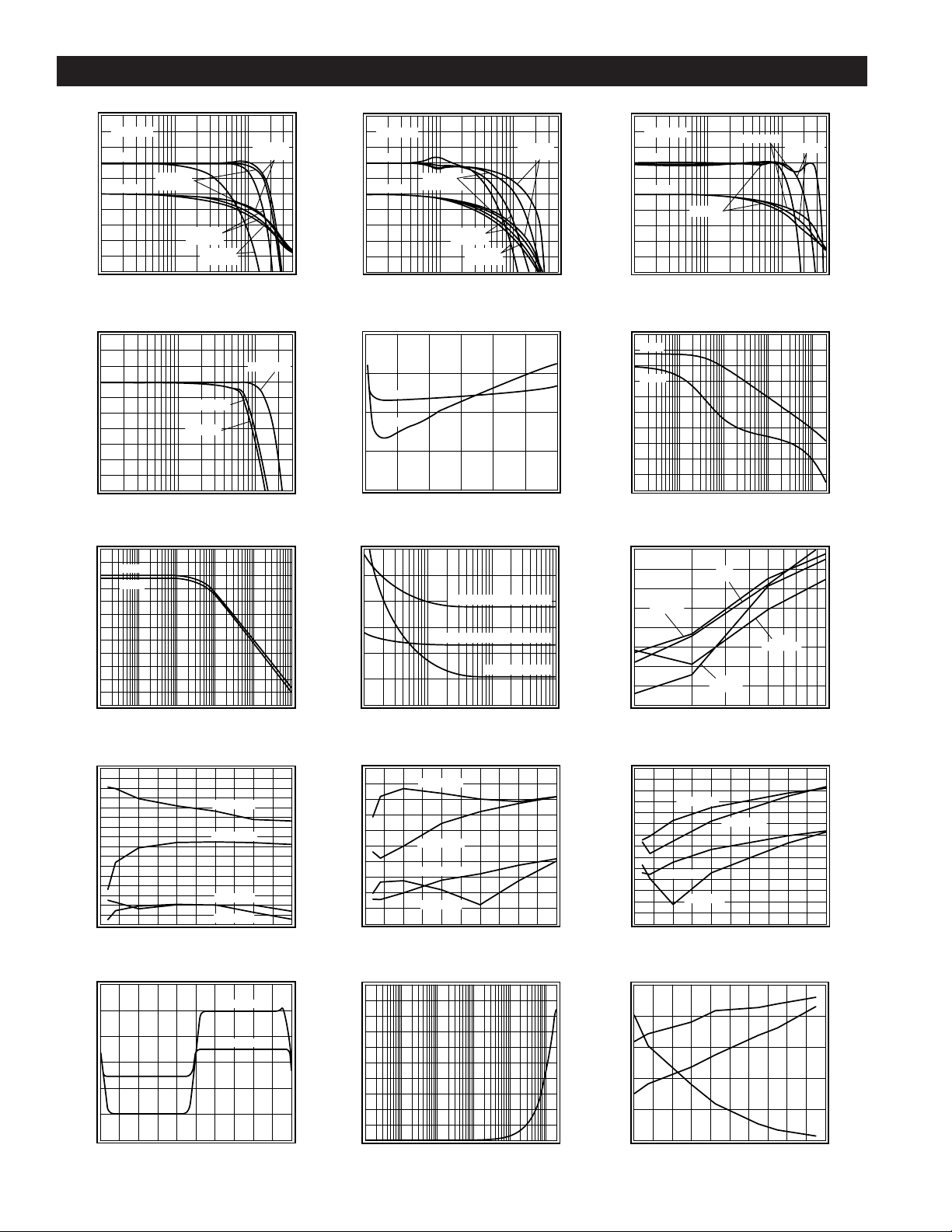
+5V T ypical Performance
(Av= +2, Rf= 750Ω,RL= 100Ω,Vs= +5V1,Vcm= VEE+ (Vs/2), RLtied to Vcm, unless specified)
Non-Inverting Frequency Response
Vo = 0.5V
pp
Gain
Av = +1
Rf = 1.2kΩ
Phase
Av = +5
Rf = 402Ω
Av = +10
10M
Rf = 200Ω
100M
Normalized Magnitude (1dB/div)
1M
Frequency (Hz)
Frequency Response vs. V
Vo = 1V
Vo = 2V
o
pp
pp
Magnitude (1dB/div)
1M
10M
100M
Frequency (Hz)
PSRR & CMRR
60
PSRR
50
CMRR
40
30
20
PSRR & CMRR (dB)
10
0
1k 10k 100M
100k 1M 10M
Frequency (Hz)
2nd & 3rd Harmonic Distortion, RL = 25Ω
-40
-45
-50
-55
-60
3rd, 10MHz
2nd, 10MHz
-65
Distortion (dBc)
-70
-75
-80
2nd, 1MHz
3rd, 1MHz
0 0.5 1 1.5 2 2.5
Output Amplitude (Vpp)
Large & Small Signal Pulse Response
Large Signal
Small Signal
Output Voltage (0.5V/div)
Time (10ns/div)
Av = +2
Rf = 649Ω
Vo = 0.1V
pp
Phase (deg)
0
-90
-180
-270
-360
-450
Inverting Frequency Response
Vo = 0.5V
pp
Gain
Av = -2
Rf = 649Ω
Phase
Av = -5
Rf = 402Ω
Av = -10
10M
Rf = 200Ω
100M
Normalized Magnitude (1dB/div)
1M
Frequency (Hz)
Gain Flatness & Linear Phase
Gain
Phase
Magnitude (0.1dB/div)
0
10
20
Frequency (MHz)
Equivalent Input Noise
3.6
3.5
3.4
3.3
Inverting Current 10.8pA/√Hz
Non-Inverting Current 7.6pA/√Hz
3.2
3.1
Noise Voltage (nV/√Hz)
3.0
10k 100k 1M 10M
Voltage 3.1nV/√Hz
Frequency (Hz)
2nd & 3rd Harmonic Distortion, RL = 100Ω
-50
3rd, 10MHz
-60
-70
2nd, 10MHz
-80
Distortion (dBc)
-90
2nd, 1MHz
3rd, 1MHz
-100
0 0.5 1 1.5 2 2.5
Output Amplitude (Vpp)
Output Impedance vs. Frequency
50
40
30
20
10
Output Impedance (Ω)
0
10k 100k 1M 10M
1k
Frequency (Hz)
Av = -1
Rf = 1kΩ
100M
180
135
90
45
0
-45
0.3
0.2
0.1
0
-0.1
30
15
11
7
3
Phase (deg)
Frequency Response vs. R
Vo = 0.5V
pp
Gain
Phase
RL = 25Ω
RL = 1kΩ
L
Phase (deg)
RL = 100Ω
0
-90
-180
Magnitude (1dB/div)
-270
-360
-450
1M
10M
100M
Frequency (Hz)
Open Loop Transimpedance Gain, Z(s)
120
Gain
100
Phase (deg)
Phase
80
60
Magnitude (dBΩ)
40
20
10k 100k 1M 10M 100M
220
180
Phase (deg)
140
100
60
20
Frequency (Hz)
2nd & 3rd Harmonic Distortion
-60
Vo = 2V
2nd
RL = 1kΩ
pp
3rd
RL = 100Ω
2nd
RL = 100Ω
3rd
RL = 1kΩ
Noise Current (pA/√Hz)
Distortion (dBc)
-70
-80
-90
-100
1M
10M
Frequency (Hz)
2nd & 3rd Harmonic Distortion, RL = 1kΩ
-50
-60
-70
3rd, 10MHz
2nd, 10MHz
-80
-90
-100
Distortion (dBc)
-110
2nd, 1MHz
3rd, 1MHz
-120
0 0.5 1 1.5 2 2.5
Output Amplitude (Vpp)
IBI, IBN, VIO vs. Temperature
-1.5 4
I
1.0 3
(mV)
IO
0.5 2
BI
I
BI
, I
V
IO
BN
(µA)
01
I
-0.5 0
Offset Voltage V
-1
BN
-1
-60 -20 20 60 100 140
Temperature (°C)
 Loading...