

NSC CLC5523IN, CLC5523IMX, CLC5523IM Datasheet
Typical Application
Variable Gain Amplifier
Circuit
CLC5523
Low-Power,Variable Gain Amplifier
March 2000
Features
■
Low power: 135mW
■
250MHz, -3dB bandwidth
■
Slew rate 1800V/ms
■
Gain flatness 0.2dB @ 75MHz
■
Rise & fall times 2.0ns
■
Low input voltage noise 4nV/ÖHz
Applications
■
Automatic gain control
■
Voltage controlled filters
■
Automatic signal leveling for A/D
■
Amplitude modulation
■
Variable gain transimpedance
General Descriptions
The CLC5523 is a low power, wideband, DC-coupled, voltagecontrolled gain amplifier. It provides a voltage-controlled gain
block coupled with a current feedback output amplifier. High
impedance inputs and minimum dependence of bandwidth on
gain make the CLC5523 easy to use in a wide range of
applications. This amplifier is suitable as a continuous gain
control element in a variety of electronic systems which benefit
from a wide bandwidth of 250MHz and high slew rate of
1800V/ms, with only 135mW of power dissipation.
Input impedances in the megaohm range on both the signal
and gain control inputs simplify driving the CLC5523 in any
application. The CLC5523 can be configured to use pin 3 as a
low impedance input making it an ideal interface for current
inputs. By using the CLC5523’s inverting configuration in which
RGis driven directly, inputs which exceed the device’s input
voltage range may be used.
The gain control input (VG), with a 0 to 2V input range, and a
linear-in-dB gain control, simplifies the implementation of AGC
circuits. The gain control circuit can adjust the gain as fast as
4dB/ns. Maximum gains from 2 to 100 are accurately and simply
set by two external resistors while attenuation of up to 80dB from
this gain can be achieved.
The extremely high slew rate of 1800V/ms and wide bandwidth
provides high speed rise and fall times of 2.0ns, with settling time
for a 2 volt step of only 22ns to 0.2%. In time domain applications
where linear phase is important with gain adjust, the internal current mode circuitry maintains low deviation of delay over a wide
gain adjust range.
CLC5523
Low-Power, Variable Gain Amplifier
© 2000 National Semiconductor Corporation http://www.national.com
Printed in the U.S.A.
+
-
CLC5523
R
f
V
o
V
in
R
g
2
3
4
1
V
G
R
L
5
-5V
8
+5V
6
7
25W
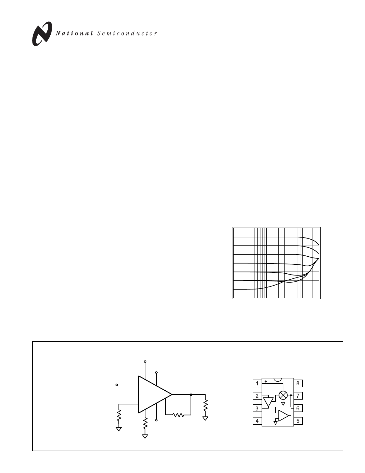
Pinout
DIP & SOIC
Frequency Response with Changes in V
30
20
10
0
-10
-20
-30
Magnitude (10dB/div)
-40
-50
1M
10M
Frequency (Hz)
g
100M
V
V
R
GND
G
IN
g
X1
+
+V
IV
-V
CC
O
CC

http://www.national.com 2
CLC5523 Electrical Characteristics
(VCC= ±5V, Rf= 1k, Rg= 100W,RL= 100W,VG= 2V; unless specified)
PARAMETERS CONDITIONS TYP MIN/MAX RATINGS UNITS NOTES
Ambient Temperature CLC5523I +25˚C25˚C -40 to 85˚C
FREQUENCY DOMAIN RESPONSE
-3dB bandwidth V
o
< 0.5V
pp
250 150 125 MHz
V
o
< 4.0V
pp
100 45 35 MHz
peaking DC to 200MHz (V
o
= 0.5Vpp) 0 0.8 2.0 dB
rolloff DC to 75MHz (V
o
= 0.5Vpp) 0.2 1.0 1.2 dB
linear phase deviation DC to 75MHz (V
o
= 0.5Vpp) 0.6 1.5 3.0 deg
gain control bandwidth V
in
= 0.2VDC, Vg= 1V
DC
95 70 60 MHz
TIME DOMAIN RESPONSE
rise and fall time 0.5V step 2.0 2.8 3.0 ns
overshoot 0.5V step 6.0 15 20 %
settling time to 0.2% 2V step 22 30 60 ns
non-inverting slew rate 4V step 700 450 400 V/ms
inverting slew rate 4V step 1800 1000 700 V/ms
gain control response rate 4 dB/nS 1
DISTORTION AND NOISE RESPONSE
2
nd
harmonic distortion 1Vpp, 5MHz -65 – – dBc
3
rd
harmonic distortion 1Vpp, 5MHz -80 – – dBc
2
nd
harmonic distortion 1Vpp, 10MHz -57 -52 -40 dBc
3
rd
harmonic distortion 1Vpp, 10MHz -75 -58 -54 dBc
input referred total noise V
g
= 2V 5 6 7 nV/ÖHz
input referred voltage noise 4 5.5 5.5 nV/ÖHz
R
g
referred current noise 36 50 60 pA/ÖHz
STATIC DC PERFORMANCE
output offset voltage 50 120 150 mV A
V
in
signal input
input voltage range R
g
open ±3.8 ±3.6 ±3.3 V
input bias current 3.0 8.0 16 mAA
input resistance 3.0 1.0 0.8 MW
input capacitance 1.0 1.5 1.7 pF
I
R
g
max
0° to 70°C 7.0 5.0 4.0 mA
I
R
g
max
-40° to 85°C 7.0 5.0 2.5 mA
signal ch. non-linearity SGNL V
o
= 2V
pp
0.04 0.1 0.2 %
gain accuracy* 0.3 0.5 0.9 dB A
V
g
gain input
input bias current 0.5 2.0 4.0 mA
input resistance 10 2.0 2.0 MW
input capacitance 1.0 1.5 1.5 pF
ground pin current 40 55 65 mA
power supply rejection ratio input-referred 57 50 46 dB
supply current R
L
= ¥ 13.5 15 16 mA A
output voltage range no load ±3.4 ±3.0 ±2.3 V
output voltage range R
L
= 100W ±3.0 ±2.5 ±2.3 V
output impedance 0.1 0.15 0.15 W
output current 80 65 50 mA
transistor count 146
*maximum gain is defined as Rf/R
g
Min/max ratings are based on product characterization and simulation. Individual parameters are tested as noted. Outgoing quality levels are
determined from tested parameters.
Absolute Maximum Ratings
supply voltage
±
7V
output current ±80mA
maximum junction temperature +150˚C
storage temperature range -65˚C to +150˚C
lead temperature (soldering 10 sec) +300˚C
ESD rating (human body model) TBD
Notes
A) I-level: spec is 100% tested at +25˚C.
1) See plot
“Gain Control Settling Time”
.
Ordering Information
Model Temp Range Description
CLC5523IN -40°C to +85°C 8-pin DIP
CLC5523IM -40°C to +85°C 8-pin Small outline
CLC5523IMX -40°C to +85°C 8-pin Small outline tape and reel
Contact the factory for other packages.
Pac kage Thermal Resistance
Package q
JC
q
JA
DIP (IN) 65°C/W 115°C/W
Small Outline (IM) 55°C/W 135°C/W

3 http://www.national.com
CLC5523 T ypical Perf ormance
(VG= +2V, Rf=1kW, Rg= 100W, RL= 100W,Vo= 0.5Vpp; unless specified)
Frequency Response (A
25
vmax
=10)
20
15
10
5
0
-5
-10
-15
Magnitude (5dB/div)
-20
-25
-30
1
10
Frequency (MHz)
Frequency Response vs. R
Magnitude
Phase
Magnitude (1dB/div)
1 10 100
L
RL = 50W
RL = 100W
Frequency (MHz)
PSRR & R
60
50
40
Magnitude (dB)
30
20
0.01 0.10 1 10 100
PSRR
R
out
out
Frequency (MHz)
Large Signal Frequency Response
V
= 1V
Inverting
Non-Inverting
Magnitude (1dB/div)
1
10
out
V
= 2V
out
V
= 4V
out
V
= 1V
out
pp
V
= 2V
out
pp
V
= 4V
out
pp
Frequency (MHz)
Gain (V/V) vs. V
10
9.0
8.0
7.0
6.0
5.0
4.0
Gain (V/V)
3.0
2.0
1.0
0
0 0.4 0.8 1.2 1.6 2.0
g
-40¡C
25¡C
85¡C
Vg Voltage (V)
100
100
pp
pp
pp
RL = 1k
Magnitude (5dB/div)
360
Phase (deg)
180
0
-180
-360
-450
100
10
R
out
(W)
1.0
0.1
0.01
Gain (dB)
Frequency Response (A
10
vmax
= 2)
5
0
-5
-10
-15
-20
-25
-30
-35
-40
-45
1
10
100
Frequency (MHz)
Frequency Response vs. R
Magnitude (1dB/div)
1 10 100
g
Rg = 500W
Rg = 10W
Rg = 33W
Rg = 100W
Frequency (MHz)
Feed-Through Isolation (VG = 0, 2)
A
= 100
40
A
= 10
vmax
20
vmax
0
-20
Gain (dB)
-40
-60
-80
1
10
100
Frequency (MHz)
Equivalent Input Noise
100
10
Voltage Noise
Current Noise
Input Voltage Noise (nVÖHz)
1
0.0001 0.001 0.01 0.1 1 10
Frequency (MHz)
Gain (dB) vs. V
20
10
0
-10
25¡C
-20
-30
-40
-50
-60
0 0.4 0.8 1.2 1.6 2.0
g
85¡C
-40¡C
Vg Voltage (V)
Magnitude (5dB/div)
1000
Input Current Noise (pAÖHz)
100
Input Voltage Noise (nVÖHz)
10
-0.5
Amplitude (0.5V/div)
-1.5
-2.5
Frequency Response (A
45
vmax
= 100)
40
35
30
25
20
15
10
5
0
-5
-10
1
10
100
Frequency (MHz)
Frequency Response vs. R
Magnitude (1dB/div)
1 10 100
Rf = 2k
Rf = 5k
f
Rf = 689W
Rf = 1k
Frequency (MHz)
Gain Flatness & Linear Phase Deviation
Vo = 2V
pp
Gain
Phase
Magnitude (0.1dB/div)
0 1530456075
Frequency (MHz)
Input Referred Total Noise
20
18
16
14
12
10
8
6
4
2
0 100 200 300 400 500
RG (W)
Large & Small Signal Pulse Response
2.5
Large
1.5
Small
0.5
Time (5ns/div)
Phase (0.5¡C/div)
0.5
0.4
Amplitude (0.1V/div)
0.3
0.2
0.1
0
-0.1
-0.2
-0.3
-0.4
-0.5

http://www.national.com 4
CLC5523 T ypical Performance
(VG= +2V, Rf=1kW, Rg= 100W,A
vmax
= 10; unless specified)
2nd Harmonic Distortion vs. Frequency
-30
Vo = 1V
-40
-50
-60
-70
-80
Distortion (dBc)
-90
-100
pp
2nd RL = 100W
2nd RL = 1k
1
10
Frequency (MHz)
Harmonic Distortion vs. Gain
-30
-50
-70
Distortion (dBc)
-90
-110
RL = 100
3rd = 10MHz
0.1 1
Vo = 100mV
2nd = 1MHz
3rd = 1MHz
Gain (Av)
Short Term Settling Time
0.2
0.1
0
(% Output Step)
o
-0.1
V
-0.2
1 100
Vo = 2Vstep
Time (ns)
DC Offset vs. Temperature
120
100
80
60
Output Offset (mV)
40
20
-60 -20 20 60 100 140
pp
2nd = 10MHz
10
10000
Input Bias Current
Output Offset Voltage
Temperature (¡C)
3rd Harmonic Distortion vs. Frequency
-40
Vo = 1V
1
pp
3rd RL = 100W
3rd RL = 1k
10
-50
-60
-70
-80
Distortion (dBc)
-90
-100
Frequency (MHz)
Input Harmonic Distortion (Av = 2)
60
VG = 1.04V
50
VG = 0.94V
= 100W
R
g
40
Distortion (dBc)
30
20
0 0.5 1.0 1.5 2.0
R
Input Voltage (V)
Long Term Settling Time
0.15
Vo = 2Vstep
0.1
0.05
0
-0.05
(% Output Step)
-0.1
o
V
-0.15
-0.2
0.001 0.01 0.1 1.0 10
Time (ms)
2.5
Input Bias Current (mA)
2.0
1.5
1.0
Intercept (dBm)
0.5
0
Harmonic Distortion vs. Output Voltage
-50
RL = 100
-60
-70
-80
-90
Distortion (dBc)
-100
-110
0 0.5 1 1.5 2
Differential Gain & Phase (NTSC)
0.05
= 250W
g
0
Gain (%)
-0.05
-0.1
-1.6 -0.8 0.8
Gain Control Settling Time
Amplitude (0.5V/div)
100
2nd Tone, 3rd Order Intermod Intercept
50
45
40
35
30
25
20
10 20 30 40 50 60 70 80
Frequency (MHz)
2nd = 10MHz
2nd = 1MHz
3rd = 10MHz
3rd = 1MHz
Output Voltage (Vpp)
Phase
0
DC Output Voltage
V
o
V
g
Time (10ns/div)
Gain
2.5
1.6
0.05
0
Phase (deg)
-0.05
-0.1
-0.15
-0.2
-0.25
 Loading...