NSC CLC430MDC, CLC430AWG-MPR, CLC430AJP, CLC430AJE-TR13, CLC430AJE Datasheet
...
N
CLC430
General Purpose 100MHz Op Amp with Disable
General Description
The CLC430 is a low-cost, wideband monolithic amplifier for general
purpose applications. The CLC430 utilizes National’s patented
current feedback circuit topology to provide an op amp with a slew rate
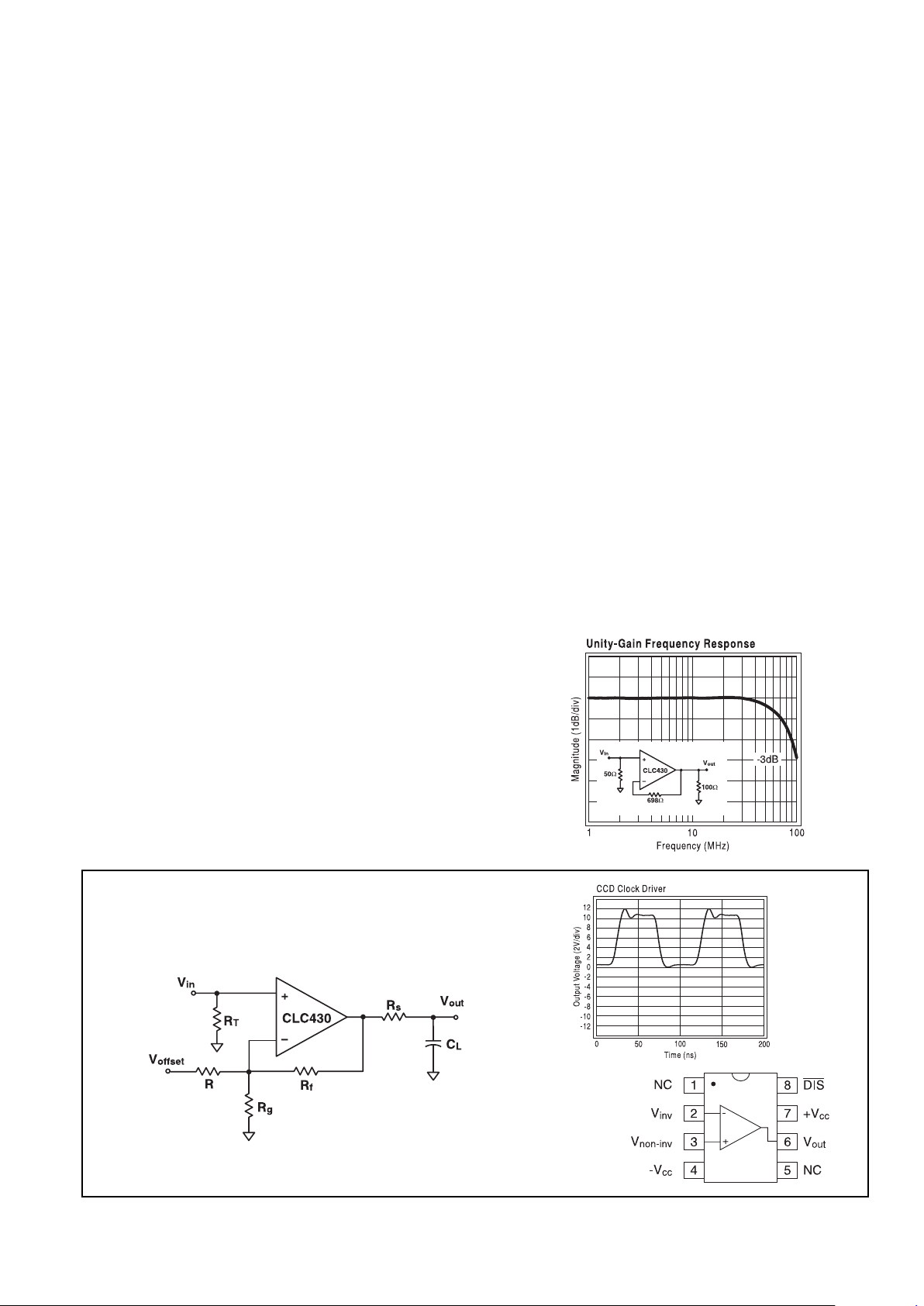
of 2000V/µs, 100MHz unity-gain bandwidth and fast output disable
function. Like all current feedback op amps, the CLC430 allows the
frequency response to be optimized (or adjusted) by the selection of
the feedback resistor. For demanding video applications, the 0.1dB
bandwidth to 20MHz and differential gain/phase of 0.03%/0.05° make
the CLC430 the preferred component for broadcast quality NTSC and
PAL video systems.
The large voltage swing (28Vpp), continuous output current (85mA)
and slew rate (2000V/µs) provide high-fidelity signal conditioning for
applications such as CCDs, transmission lines and low impedance
circuits. Even driving loads of 100Ω, the CLC430 provides very low
2nd and 3rd harmonic distortion at 1MHz (-76/-82dBc).
Video distribution, multimedia and general purpose applications will
benefit from the CLC430’s wide bandwidth and disable feature. Power
is reduced and the output becomes a high impedance when disabled.
The wide gain range of the CLC430 makes this general purpose op
amp an improved solution for circuits such as active filters, differential-to-single-ended drivers, DAC transimpedance amplifiers and
MOSFET drivers.
June 1999
Features
■ 0.1dB gain flatness to 20MHz (A
v
=+2)
■ 100MHz bandwidth (A
v
=+1)
■ 2000V/µs slew rate
■ 0.03%/0.05° differential gain/phase
■ ±5V, ±15V or single supplies
■ 100ns disable to high-impedance output
■ Wide gain range
■ Low cost
Applications
■ Video distribution
■ CCD clock driver
■ Multimedia systems
■ DAC output buffers
■ Imaging systems
CLC430
General Purpose 100MHz Op Amp with Disable
Pinout
DIP & SOIC
Typical Application
CCD Clock Driver
1999 National Semiconductor Corporation http://www.national.com
Printed in the U.S.A.

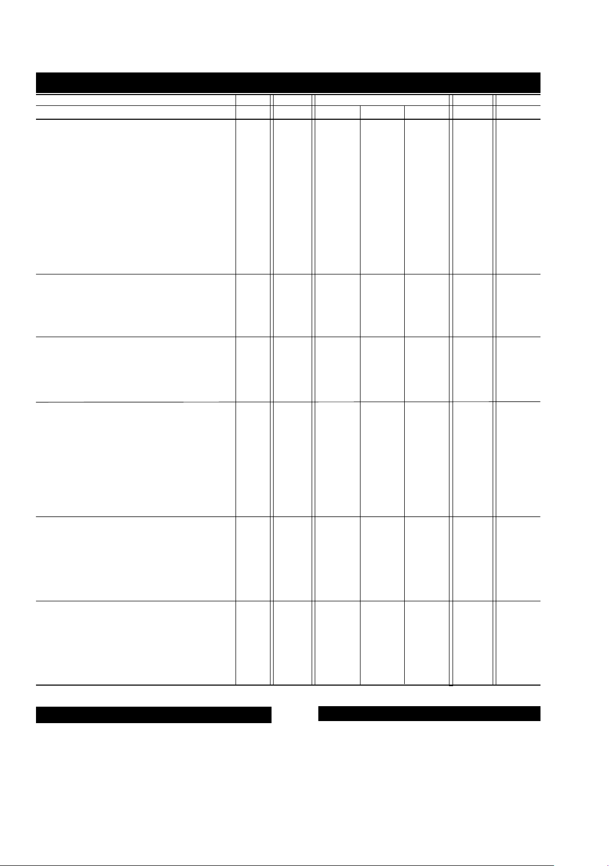
CLC430 Electrical Characteristics (V
CC
= ±15V; A
V
= +2V/V; R
f
=604
ΩΩ
ΩΩ
Ω; R
L
= 100
ΩΩ
ΩΩ
Ω; unless noted)
PARAMETERS CONDITIONS V
cc
TYP MIN/MAX RATINGS UNITS NOTES
Ambient Temperature CLC430 25°C 25°C 0 to 70°C -40 to 85°C
FREQUENCY DOMAIN RESPONSE
unity-gain bandwidth V
out
< 1.0V
pp
±15 100 MHz
small-signal bandwidth V
out
< 1.0V
pp
±15 75 50 45 42 MHz
V
out
< 1.0V
pp
±5 55 35 MHz
0.1dB bandwidth V
out
< 1.0V
pp
±15 2 0 7 MHz
V
out
< 1.0V
pp
±5 16 MHz
large-signal bandwidth V
out
= 10V
pp
30 22 20 19 MHz
gain flatness V
out
< 1.0V
pp
peaking DC to 10MHz 0.0 0.1 0.2 0.2 dB
rolloff DC to 20MHz 0.1 0.7 1.0 1.2 dB
linear phase deviation DC to 20MHz 0.5 1.8 2.0 2.1 °
differential gain 4.43MHz, R
L
=150Ω ±15 0.03 0.05 0.06 0.06 %
4.43MHz, R
L
=150Ω ±5 0.03 0.05 %
differential phase 4.43MHz, RL=150Ω ±15 0.05 0.09 0.12 0.13 °
4.43MHz, R
L
=150Ω ±5 0.09 0.19 °
TIME DOMAIN RESPONSE
rise and fall time 2V step 5 7 7 7 n s
10V step 10 1 4 1 4 14 ns
settling time to 0.05% 2V step 35 5 0 5 5 5 5 ns
overshoot 2V step 5 15 1 5 15 %
slew rate 20V step 20 00 1500 1450 1450 V/µs
DISTORTION AND NOISE RESPONSE
2
nd
harmonic distortion 1Vpp,1MHz, RL=500 -89 dBc
3
rd
harmonic distortion 1Vpp,1MHz, RL=500 -92 dBc
input voltage noise >1MHz 3.0 3.5 3.7 3.8 nV/√Hz
non-inverting input current noise >1MHz 3.2 6.0 6.3 6.8 pA/√Hz
inverting input current noise >1MHz 15 18 20 21 pA/√Hz
DC PERFORMANCE
input offset voltage ±15 1.0 7.5 9.0 10.0 mV A
average drift 25 --- 50 5 0 µV/ C
input bias current non-inverting ±15,±5 3 14 16 20 µAA
average drift 10 --- 100 1 00 nA/°C
input bias current inverting ±15,±5 3 14 15 17 µAA
average drift 10 --- 60 9 0 nA/°C
power-supply rejection ratio DC 62 56 54 53 dB
common-mode rejection ratio DC 62 54 5 3 5 2 dB
supply current R
L
= ∞ ±15,±5 11, 8.5 12 13 14.5 mA A
disabled R
L
= ∞ ±15,±5 1.5 2.0 2.2 2.4 mA A
SWITCHING PERFORMANCE
turn on time 2 0 0 300 320 340 ns
turn off time (Note 2) 100 200 200 200 ns
off isolation 10MHz 59 5 6 56 56 dB
high input voltage V
IH
±15 11.8 12.5 12.7 V
±5 1.8 2.5 2.7 V
low input voltage V
IL
±15 10.8 10.5 10.0 V
±5 0.8 0.6 0.1 V
MISCELLANEOUS PERFORMANCE
Non-inverting input resistance 8.0 3.0 2.5 1.7 MΩ
Non-inverting input capacitance 0.5 1.0 1.0 1.0 pF
input voltage range common mode ±15 ±12.5 ±12.3 ±12.1 ±11.8 V
common mode ±5 ±2.5 ±2.3 ±2.2 ±1.9 V
output voltage range R
L
= ∞ ±15 ±14 ±13.7 ±13.7 ±13.6 V
RL= ∞ ±5 ±4.0 ±3.9 ±3.8 ±3.7 V
output current ±85 ± 60 ± 50 ± 45 mA
Min/max ratings are based on product characterization and simulation. Individual parameters are tested as noted. Outgoing quality levels
are determined from tested parameters.
http://www.national.com 2
Absolute Maximum Ratings
supply voltage ±16.5V
short circuit current (note 1)
common-mode input voltage ±V
cc
maximum junction temperature +150°C
storage temperature -65°C to+150°C
lead temperature (soldering 10 sec) +300°C
ESD rating (human body model) 4000V
Notes
A) J-level: spec is 100% tested at +25°C.
1)Output is short circuit protected to ground, however
maximum reliability is obtained if output current does not
exceed 125mA.
2) To>50dB attenuation @ 10MHz.

3 http://www.national.com
 Loading...