NSC CLC428MDC, CLC428AJP, CLC428AJE-TR13, CLC428AJE, 5962-9470801MPA Datasheet

N
CLC428
Dual Wideband, Low-Noise, Voltage Feedback Op Amp
General Description
The CLC428 is a very high-speed dual op amp that offers a traditional
voltage-feedback topology featuring unity-gain stability and slewenhanced circuitry. The CLC428’s ultra low noise and very low
harmonic distortion combine to form a very wide dynamic-range op
amp that operates from a single (5 to 12V) or dual (±5V) power supply.
Each of the CLC428’s closely matched channels provides a 160MHz
unity-gain bandwidth with an ultra low input voltage noise density
(2nV/√Hz). Very low 2nd/3rd harmonic distortion (-62/-72dBc) as well
as high channel-to-channel isolation (-62dB) make the CLC428 a
perfect wide dynamic-range amplifier for matched I/Q channels.
With its fast and accurate settling (16ns to 0.1%), the CLC428 is also
a excellent choice for wide-dynamic range, anti-aliasing filters
to buffer the inputs of hi-resolution analog-to-digital converters.
Combining the CLC428’s two tightly-matched amplifiers in a single
eight-pin SOIC reduces cost and board space for many composite
amplifier applications such as active filters, differential line drivers/
receivers, fast peak detectors and instrumentation amplifiers.
To reduce design times and assist in board layout, the CLC428 is
supported by an evaluation board and a SPICE simulation model
available from National Semiconductor.
June 1999
Features
■ Wide unity-gain bandwidth: 160MHz
■ Ultra-low noise: 2.0nV/√Hz
■ Low distortion: -78dBc 2nd (2MHz)
-62/-72dBc (10MHz)
■ Settling time: 16ns to 0.1%
■ Supply voltage range: ±2.5 to ±5 or
single supply
■ High output current: ±80mA
Applications
■ General purpose dual op amp
■ Low noise integrators
■ Low noise active filters
■ Diff-in/diff-out instrumentation amp
■ Driver/receiver for transmission systems
■ High-speed detectors
■ I/Q channel amplifiers
CLC428
Dual Wideband, Low-Noise, Voltage Feedback Op Amp
Pinout
DIP & SOIC
1
2
3
4
8
7
6
5
V
out
1
V
inv
1
V
non-inv
1
-Vcc
+V
cc
V
out
2
V
inv
2
V
non-inv
2
+
+
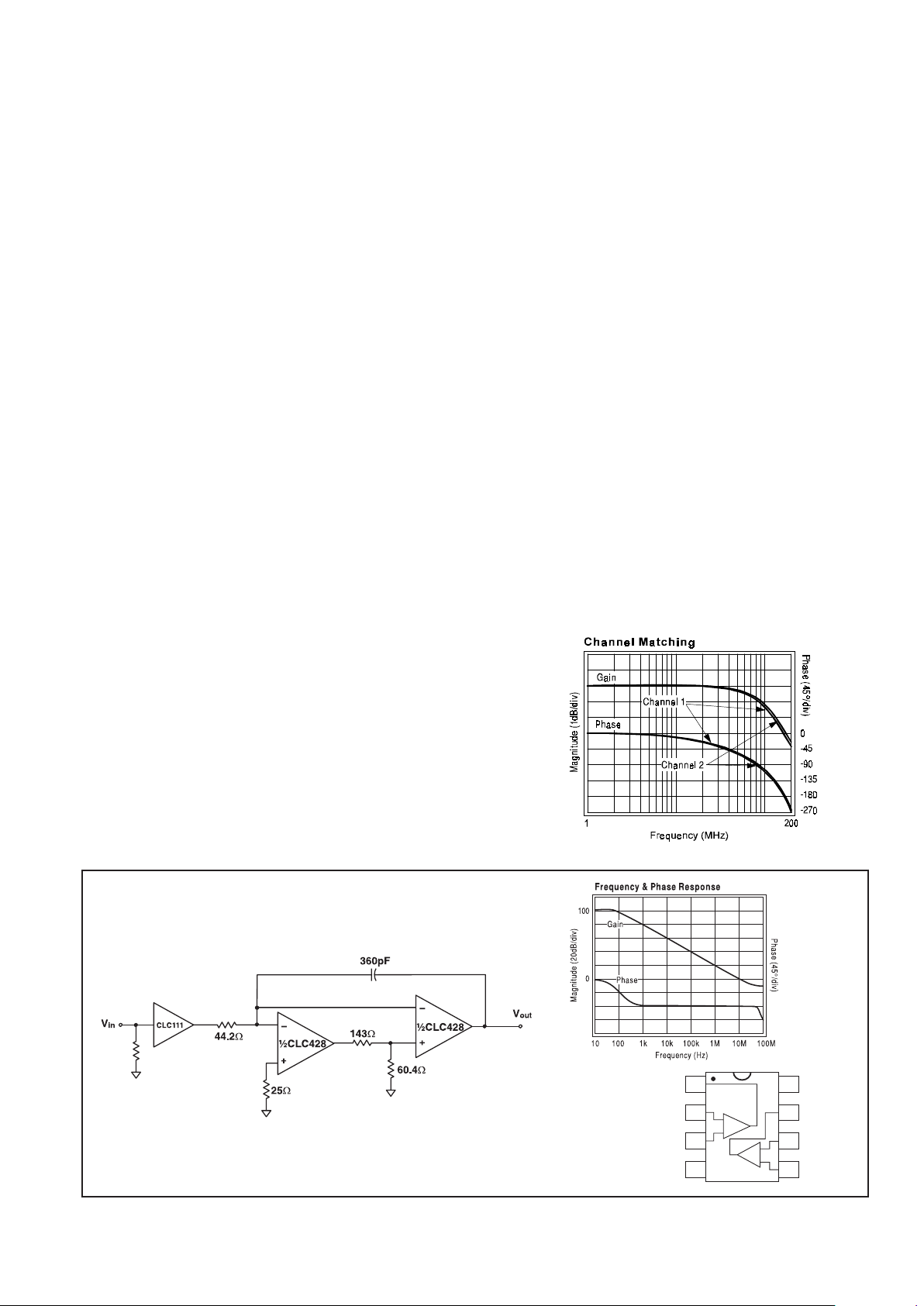
Typical Application
5-Decade Integrator
1999 National Semiconductor Corporation http://www.national.com
Printed in the U.S.A.

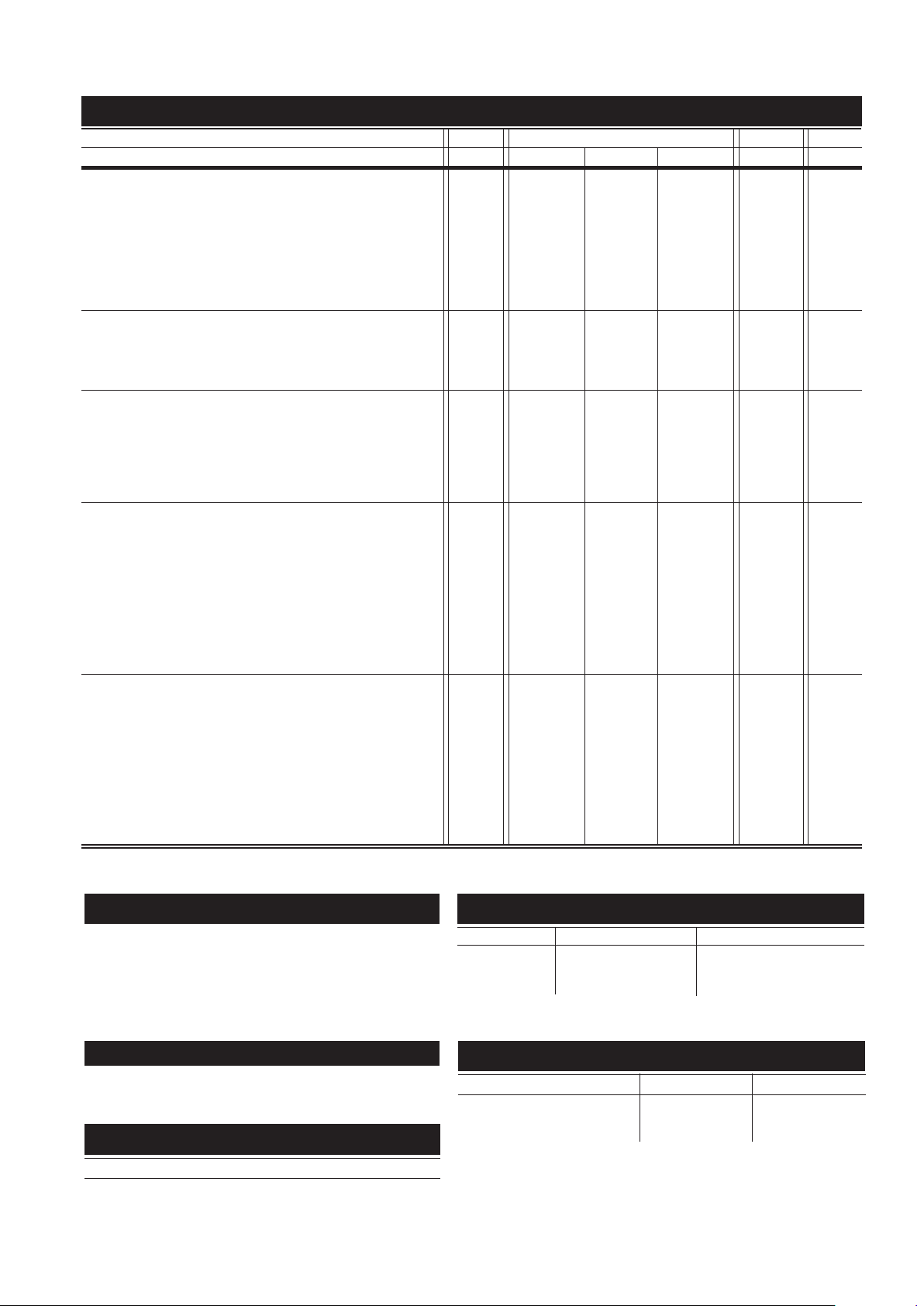
CLC428 Electrical Characteristics (V
CC
= ±5V; A
V
= +2V/V; R
f
=100
ΩΩ
ΩΩ
Ω; R
g
=100
ΩΩ
ΩΩ
Ω; R
L
= 100
ΩΩ
ΩΩ
Ω; unless noted;
PARAMETERS CONDITIONS TYP MIN/MAX RATINGS UNITS NOTES
Ambient Temperature CLC428 +25°C +25°C 0 to +70°C -40 to +85°C
FREQUENCY DOMAIN RESPONSE
gain bandwidth product V
out
< 0.5V
pp
135 100 80 70 MHz
-3dB bandwidth, Av=+1 V
out
< 0.5V
pp
160 120 90 80 MHz
Av=+2 V
out
< 0.5V
pp
80 50 40 35 MHz
V
out
< 5.0V
pp
40 25 22 20 MHz
gain flatness V
out
< 0.5V
pp
peaking DC to 200MHz 0.0 0.6 0.8 1.0 d B
rolloff DC to 20MHz 0.05 0.5 0.7 0.7 dB
linear phase deviation DC to 20MHz 0.2 1.0 1.5 1.5 °
TIME DOMAIN RESPONSE
rise and fall time 1V step 5.5 7.5 9.0 10.0 ns
settling time 2V step to 0.1% 16 20 24 24 ns
overshoot 1V step 1 5 10 10 %
slew rate 5V step 500 300 275 2 50 V/µs
DISTORTION AND NOISE RESPONSE
2
nd
harmonic distortion 1Vpp,10MHz - 62 - 5 0 - 45 - 43 dBc
3rd harmonic distortion 1Vpp,10MHz - 72 -60 - 56 - 5 6 dBc
equivalent input noise
voltage 1MHz to 100MHz 2.0 2.5 2.8 2.8 nV/ √Hz
current 1MHz to 100MHz 2.0 3.0 3.6 4.6 pA/√Hz
crosstalk input referred, 10MHz - 62 - 58 - 5 8 - 5 8 dB
STATIC DC PERFORMANCE
open-loop gain 60 56 50 50 dB
input offset voltage 1.0 2.0 3.0 3.5 m V A
average drift 5 --- 15 20 µV/°C
input bias current 1.5 25 40 65 µAA
average drift 15 0 --- 600 700 nA/ °C
input offset current 0.3 3 5 5 µA
average drift 5 --- 25 50 nA/°C
power supply rejection ratio 66 60 55 55 dB
common-mode rejection ratio 63 57 52 52 dB
supply current per channel, R
L
= ∞ 11 12 13 15 mA A
MISCELLANEOUS PERFORMANCE
input resistance common-mode 500 250 125 125 kΩ
differential-mode 200 50 25 2 5 kΩ
input capacitance common-mode 2.0 3.0 3.0 3.0 pF
differential-mode 2.0 3.0 3.0 3.0 pF
output resistance closed loop 0.05 0.1 0.2 0.2 Ω
output voltage range R
L
= ∞ ± 3.8 ± 3.5 ± 3.3 ± 3.3 V
RL=100Ω ± 3.5 ± 3.2 ± 2.6 ± 1.3 V
input voltage range common mode ± 3.7 ± 3.5 ± 3.3 ± 3.3 V
output current ± 70 ± 5 0 ± 4 0 ± 20 mA
Min/max ratings are based on product characterization and simulation. Individual parameters are tested as noted. Outgoing quality levels are
determined from tested parameters.
Ordering Information
supply voltage ±7V
short circuit current (note 1)
common-mode input voltage ±V
cc
differential input voltage ±10V
maximum junction temperature +150°C
storage temperature -65°C to+150°C
lead temperature (soldering 10 sec) +300°C
Absolute Maximum Ratings
Model Temperature Range Description
CLC428AJP -40°C to +85°C 8-pin PDIP
CLC428AJE -40°C to +85°C 8-pin SOIC
CLC428A8B -55°C to +125°C 8-pin CerDIP, MIL-STD-883
DESC SMD number: 5962-94708
http://www.national.com 2
Package θ
jc
θ
jA
Plastic (AJP) 60°C/W 115°C/W
Surface Mount (AJE) 40°C/W 115°C/W
CerDIP 25°C/W 115°C/W
Pa ckage Thermal Resistance
Notes
A)J-level: spec is 100% tested at +25°C, sample tested at +85°C.
1) Output is short circuit protected to ground, however maximum
reliability is obtained if output current does not exceed 160mA.
Transistor count 104
Reliability Information

3 http://www.national.com
 Loading...