NSC 5962R9561901VXA, 54ACTQ16244MDA Datasheet

54ACTQ16244
16-Bit Buffer/Line Driver with TRI-STATE
®
Outputs
General Description
The ’ACTQ16244 contains sixteen non-inverting buffers with
TRI-STATE outputs designed to be employed as a memory
and address driver, clock driver, or bus oriented transmitter/
receiver. The device is nibble controlled. Each nibble has
separate TRI-STATE control inputs which can be shorted together for full 16-bit operation.
The ’ACTQ16244 utilizes NSC Quiet Series technology to
guarantee quiet output switching and improved dynamic
threshold performance. FACTQuiet Series
®
features GTO
®
output control for superior performance.
Features
n Utilizes NSC FACT Quiet Series technology
n Guaranteed simultaneous switching noise level and
dynamic threshold performance
n Separate control logic for each byte and nibble
n 16-bit version of the ’ACTQ244
n Outputs source/sink 24 mA
n Standard Microcircuit Drawing (SMD) 5962-9561901
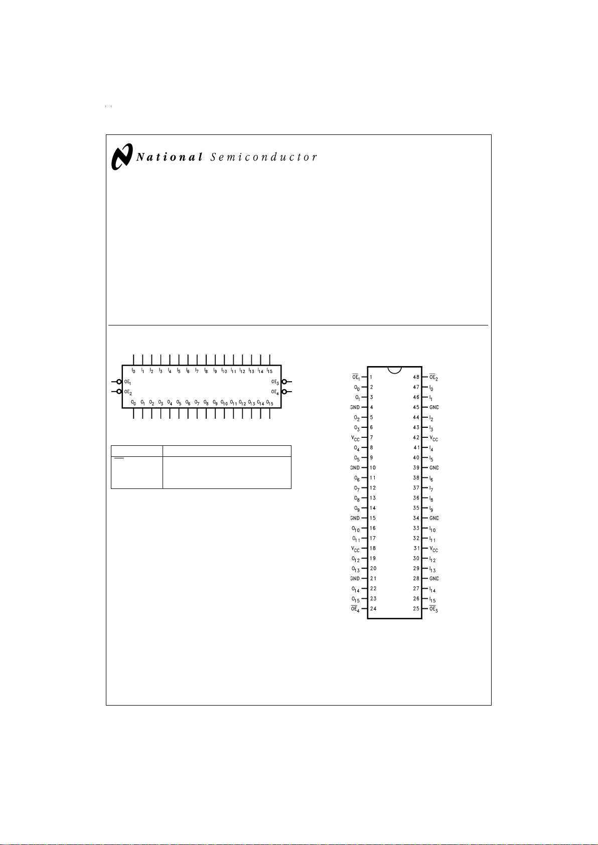
Logic Symbol
Pin Description
Pin Names Description
OE
n
Output Enable Input (Active Low)
I
0–I15
Inputs
O
0–O15
Outputs
Connection Diagram
GTO™is a trademark of National Semiconductor Corporation.
TRI-STATE
®
is a registered trademark of National Semiconductor Corporation.
FACT
™
and FACT Quiet Series™are trademarks of Fairchild Semiconductor Corporation.
DS010925-1
Pin Assignment for CERPAK
DS010925-2
September 1998
54ACTQ16244 16-Bit Buffer/Line Driver with TRI-STATE Outputs
© 1998 National Semiconductor Corporation DS010925 www.national.com

Functional Description
The ’ACTQ16244 contains sixteen non-inverting buffers with
TRI-STATE standard outputs. The device is nibble (4 bits)
controlled with each nibble functioning identically, but independent of the other. The control pins can be shorted together to obtain full 16-bit operation. The TRI-STATE outputs
are controlled by an Output Enable (OE
n
) input for each
nibble. When OEnis LOW, the outputs are in 2-state mode.
When OEnis HIGH, the outputs are in the high impedance
mode, but this does not interfere with entering new data into
the inputs.
Truth Tables
Inputs Outputs
OE
1
I0–I
3
O0–O
3
LL L
LH H
HX Z
Inputs Outputs
OE
3
I8–I
11
O8–O
11
LL L
LH H
Inputs Outputs
OE
3
I8–I
11
O8–O
11
HX Z
Inputs Outputs
OE
2
I4–I
7
O4–O
7
LL L
LH H
HX Z
Inputs Outputs
OE
4
I12–I
15
O12–O
15
LL L
LH H
HX Z
H
=
High Voltage Level
L=Low Voltage Level
X=Immaterial
Z=High Impedance
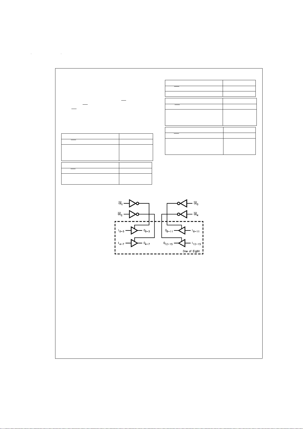
Logic Diagram
DS010925-3
www.national.com 2
 Loading...