

Page 1

PAMS Technical Documentation
RAE-5 Series PDA
9. Schematic diagrams
Issue 1 04/2002
Copyright 2002. Nokia Corporation. All Rights Reserved.
Page 2
PAMS
RAE-5
Technical Documentation
Amendment
Number
Date Inserted By Comments
04/2002 OJuntunen
9. Schematic diagrams
AMENDMENT RECORD SHEET
Issue 1 04/2002
Page 09 – 2
Page 3

PAMS
RAE-5
Technical Documentation
CONTENTS –Schematic Diagrams
Block Diagram of UL1_07 QWERTY keypad (Version 0.0 Edit 139)
09 – 4. . . . . . . . . . . . . . . . . . . . . . . . . . . . . . . . . . . . . . . . . . . . . . . . . . . . . . .
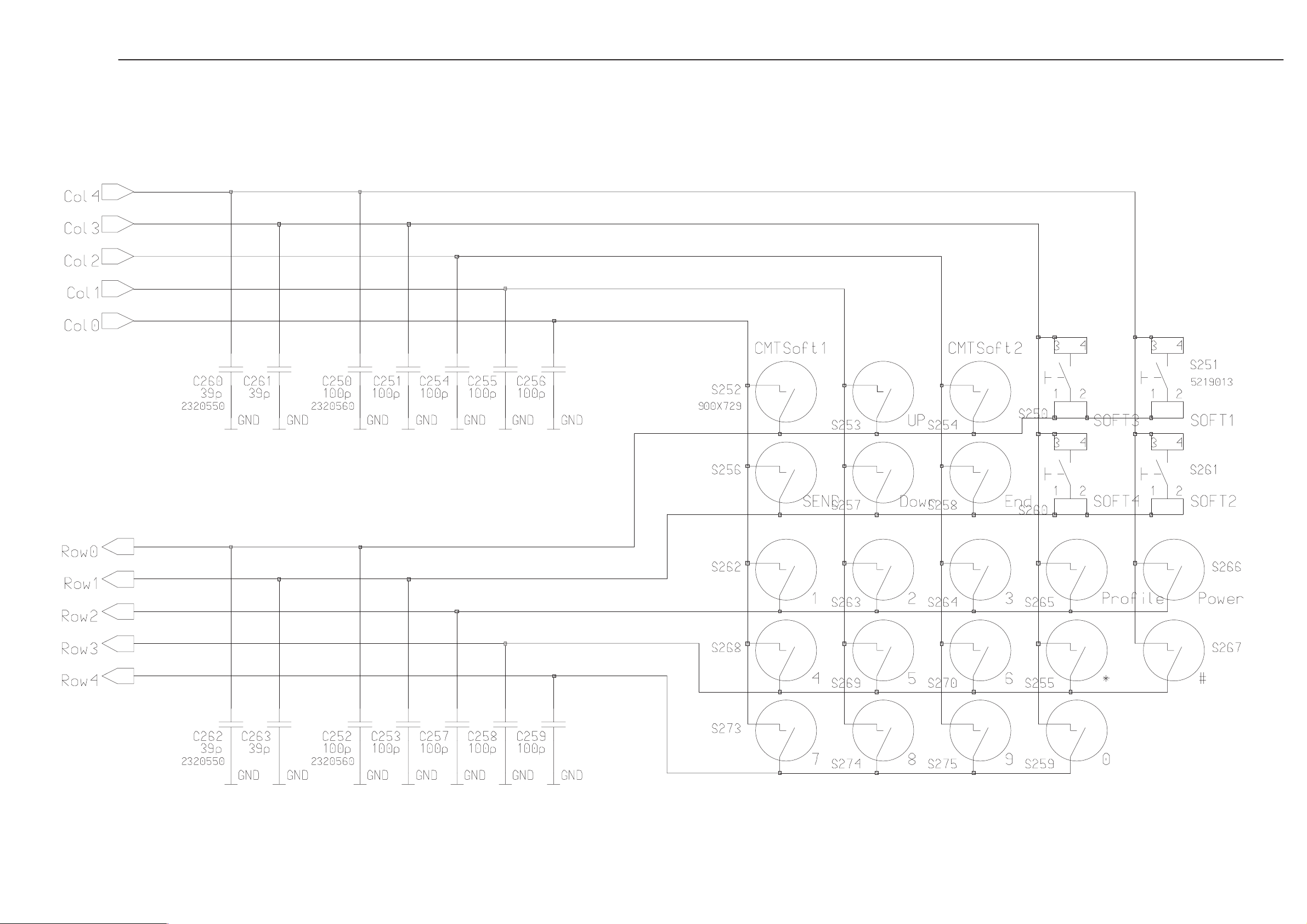
Block Diagram of UL1_07 CMT keyboard and PDA soft keys (Version 0.0 Edit 22)
09 – 5. . . . . . . . . . . . . . . . . . . . . . . . . . . . . . . . . . . . . . . . . . . . . . . . . . . . . . .
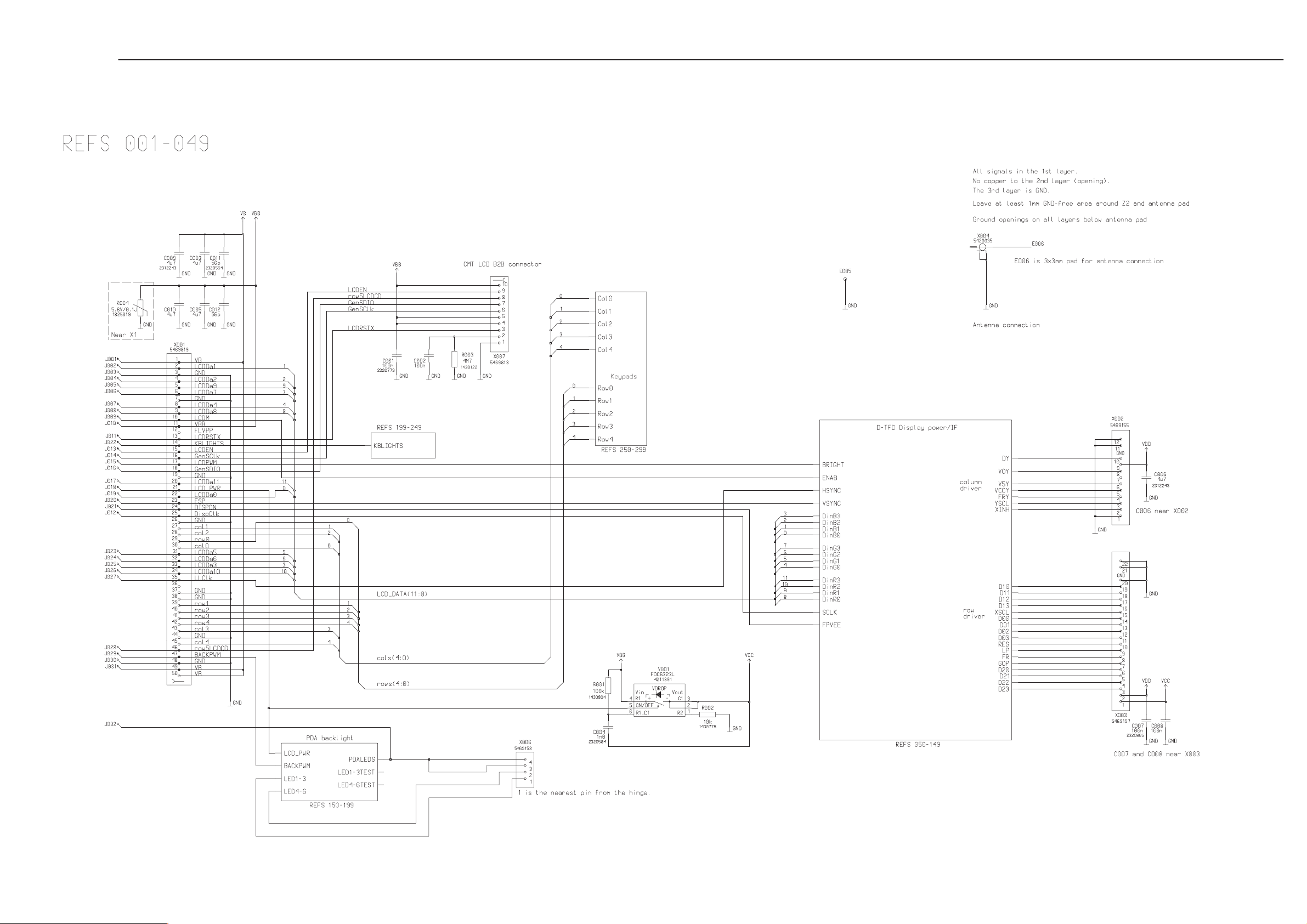
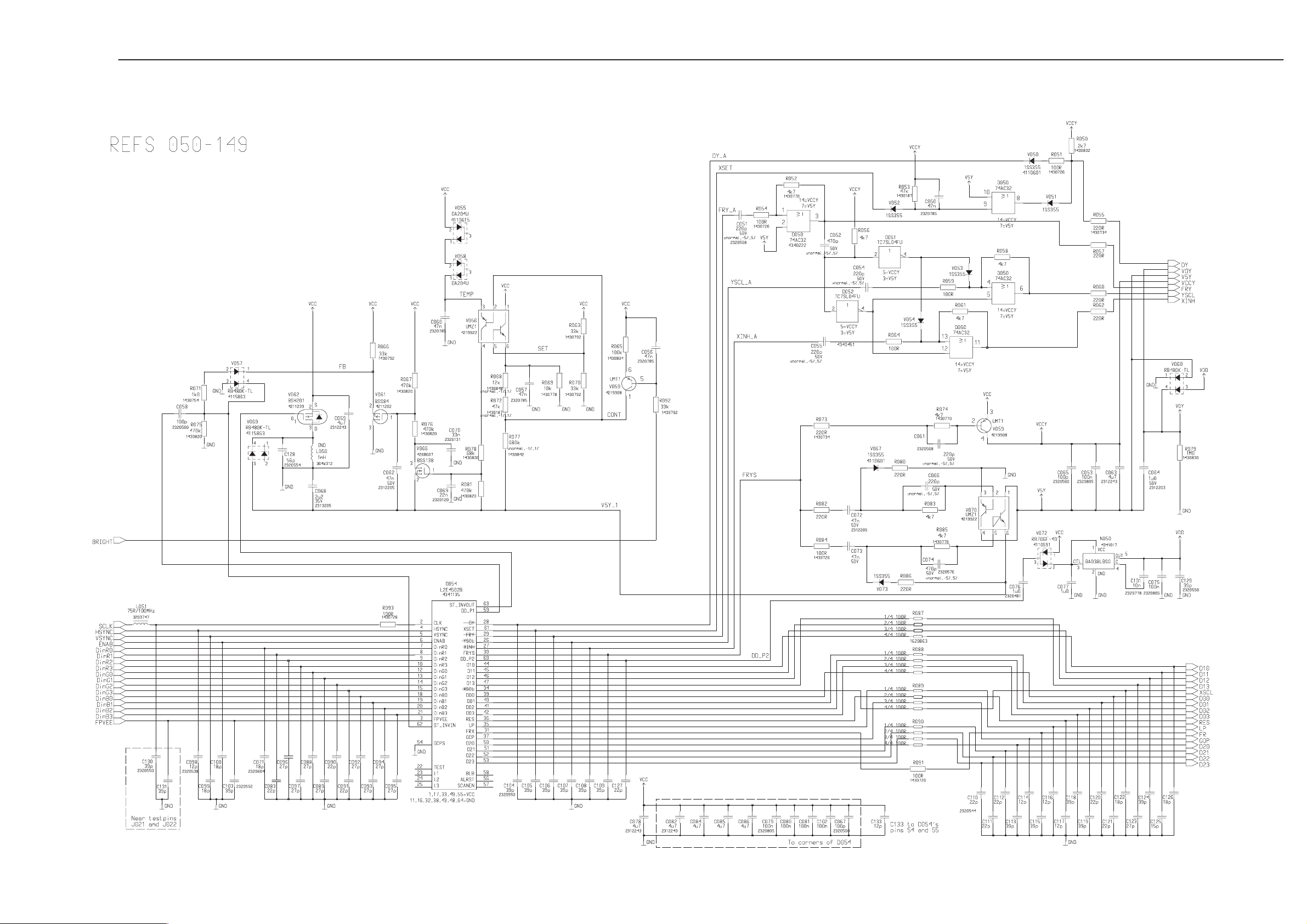
Circuit Diagram of UL1_07 D–TFD power interface (Version 0.0 Edit 126)
09 – 6. . . . . . . . . . . . . . . . . . . . . . . . . . . . . . . . . . . . . . . . . . . . . . . . . . . . . . .
Circuit Diagram of UL1_07 CMT UI LEDs (Version 0.0 Edit 28) 09 – 7
Circuit Diagram of UL1_07 PDA backlight (Version 0.0 Edit 40) 09 – 8
Parts Placement Diagram of UL1_07 1/2 09 – 9. . . . . . . . . . . . . . . . . .
Parts Placement Diagram of UL1_07 2/2 09 – 10. . . . . . . . . . . . . . . . . .
Block Diagram of KL8_05 System (Version 0.2 Edit 114) 09 – 11. . . .
Circuit Diagram of KL8_05 System Connector (Version 0.0 Edit 125)
09 – 12. . . . . . . . . . . . . . . . . . . . . . . . . . . . . . . . . . . . . . . . . . . . . . . . . . . . . . .
9. Schematic diagrams
Page No
Circuit Diagram of KL8_05 Audio RFI (Version 0.0 Edit 144) 09 – 13.
Circuit Diagram of KL8_05 CPU (Version 0.0 Edit 167) 09 – 14. . . . . .
Circuit Diagram of KL8_05 IRDA (Version 0.0 Edit 167) 09 – 15. . . . .
Circuit Diagram of KL8_05 memories (Version 0.0 Edit 106) 09 – 16.
Circuit Diagram of KL8_05 MMC (Version 0.0 Edit 73) 09 – 17. . . . . . .
Circuit Diagram of KL8_05 Power (Version 0.0 Edit 216) 09 – 18. . . . .
Circuit Diagram of KL8_05 User interface (Version 0.0 Edit 83) 09 – 19
Circuit Diagram of KL8_05 BB/RF Connector (Version 0.2 Edit 114)
09 – 20. . . . . . . . . . . . . . . . . . . . . . . . . . . . . . . . . . . . . . . . . . . . . . . . . . . . . . .
Circuit Diagram of KL8_05 RF (Version 0.2 Edit 197) 09 – 21. . . . . . . .
Parts Placement Diagram of KL8_05 1/2 09 – 22. . . . . . . . . . . . . . . . . .
Parts Placement Diagram of KL8_05 2/2 09 – 23. . . . . . . . . . . . . . . . . .
Issue 1 04/2002
Page 09 – 3
Page 4
PAMS
RAE-5
Technical Documentation
Block Diagram of UL1_07 QWERTY keypad (Version 0.0 Edit 139)
9. Schematic diagrams
UL1_06
Issue 1 04/2002
Page 09 – 4
Page 5
PAMS
RAE-5
Technical Documentation
Block Diagram of UL1_07 CMT keyboard and PDA soft keys (Version 0.0 Edit 22)
9. Schematic diagrams
Issue 1 04/2002
Page 09 – 5
Page 6
PAMS
RAE-5
Technical Documentation
Circuit Diagram of UL1_07 D–TFD power interface (Version 0.0 Edit 126)
9. Schematic diagrams
UL1_06
Issue 1 04/2002
Page 09 – 6
Page 7
PAMS
RAE-5
Technical Documentation
Circuit Diagram of UL1_07 CMT UI LEDs (Version 0.0 Edit 28)
9. Schematic diagrams
Issue 1 04/2002
Page 09 – 7
Page 8

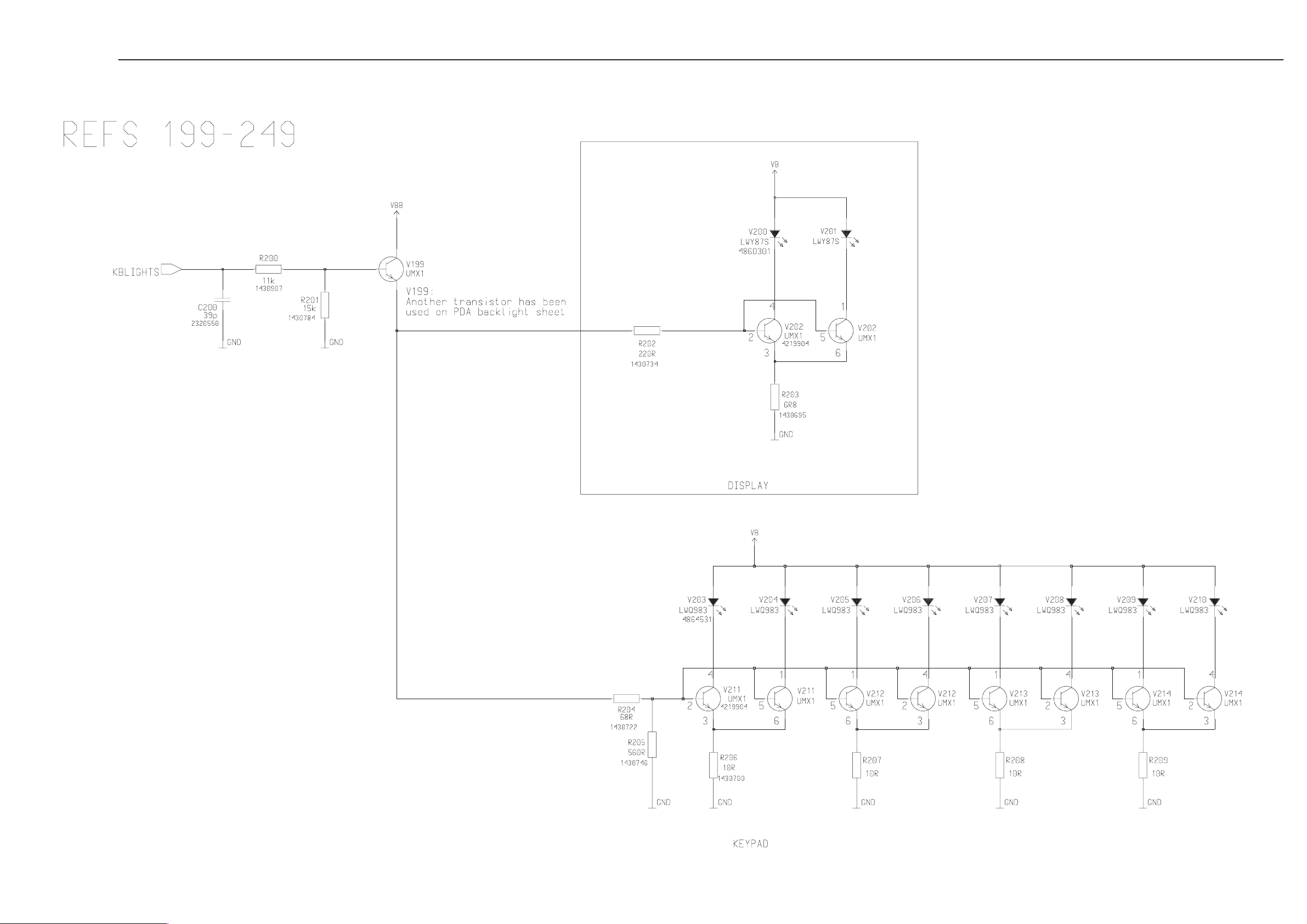
PAMS
RAE-5
Technical Documentation
Circuit Diagram of UL1_07 PDA backlight (V ersion 0.0 Edit 40)
9. Schematic diagrams
UL1_06
Issue 1 04/2002
Page 09 – 8
Page 9

PAMS
RAE-5
Technical Documentation
Parts Placement Diagram of UL1_07 1/2
9. Schematic diagrams
Issue 1 04/2002
Page 09 – 9
Page 10

PAMS
RAE-5
Technical Documentation
Parts Placement Diagram of UL1_07 2/2
9. Schematic diagrams
Issue 1 04/2002
Page 09 – 10
Page 11

PAMS
RAE-5
Technical Documentation
Block Diagram of KL8_05 System (Version 0.2 Edit 114)
9. Schematic diagrams
Issue 1 04/2002
Page 09 – 11
Page 12

PAMS
RAE-5
Technical Documentation
Circuit Diagram of KL8_05 System Connector (Version 0.0 Edit 125)
9. Schematic diagrams
Linda HWID K3110
KL8_05 syscon
Issue 1 04/2002
Page 09 – 12
Page 13

PAMS
RAE-5
Technical Documentation
Circuit Diagram of KL8_05 Audio RFI (Version 0.0 Edit 144)
9. Schematic diagrams
Linda HWID K3110
KL8_05 audio_rfi
Issue 1 04/2002
Page 09 – 13
Page 14

PAMS
RAE-5
Technical Documentation
Circuit Diagram of KL8_05 CPU (Version 0.0 Edit 167)
9. Schematic diagrams
KL8_05 cpu
Linda HWID K3110
Issue 1 04/2002
Page 09 – 14
Page 15

PAMS
RAE-5
Technical Documentation
Circuit Diagram of KL8_05 IRDA (Version 0.0 Edit 167)
9. Schematic diagrams
Issue 1 04/2002
Page 09 – 15
Page 16

PAMS
RAE-5
Technical Documentation
Circuit Diagram of KL8_05 memories (Version 0.0 Edit 106)
9. Schematic diagrams
Linda HWID K3110
KL8_05 memories
Issue 1 04/2002
Page 09 – 16
Page 17

PAMS
RAE-5
Technical Documentation
Circuit Diagram of KL8_05 MMC (Version 0.0 Edit 73)
9. Schematic diagrams
Issue 1 04/2002
Page 09 – 17
Page 18

PAMS
RAE-5
Technical Documentation
Circuit Diagram of KL8_05 Power (Version 0.0 Edit 216)
Linda HWID K3110
9. Schematic diagrams
KL8_05 power
Not assembled
Not assembled
Issue 1 04/2002
Page 09 – 18
Page 19

PAMS
RAE-5
Technical Documentation
Circuit Diagram of KL8_05 User interface (Version 0.0 Edit 83)
9. Schematic diagrams
Linda HWID K3110
KL8_05 ui
Issue 1 04/2002
Page 09 – 19
Page 20

PAMS
RAE-5
Technical Documentation
Circuit Diagram of KL8_05 BB/RF Connector (Version 0.2 Edit 114)
9. Schematic diagrams
Issue 1 04/2002
Page 09 – 20
Page 21

PAMS
RAE-5
Technical Documentation
Circuit Diagram of KL8_05 RF (Version 0.2 Edit 197)
Wide connection
below component
LAYER_4
Wide connection
below component
9. Schematic diagrams
KL8_05
Not assembled
LAYER_4
LAYER_4
Not assembled
Not assembled
Wide connection
below component
Wide connection
below component
Not assembled
Not assembled
Not assembled
Not assembled
Charge pump
TOO HIGH VOLT
Modulator
VCTCXO
LNA2+mixer+DTOS
Dividers+LO–buffers+prescaler+VCO
Vdd_bb+LNA
Issue 1 04/2002
Not assembled
Page 09 – 21
Page 22

PAMS
RAE-5
Technical Documentation
Parts Placement Diagram of KL8_05 1/2
9. Schematic diagrams
Issue 1 04/2002
Page 09 – 22
Page 23

PAMS
RAE-5
Technical Documentation
Parts Placement Diagram of KL8_05 2/2
9. Schematic diagrams
Issue 1 04/2002
Page 09 – 23
 Loading...