

Page 1

PAMS Technical Documentation
RAE-3 Series PDA
4. User Interfaces
Issue 1 06/01
Copyright 2001. Nokia Mobile Phones. All Rights Reserved.
Page 2
RAE-3
PAMS
4. User Interfaces
Amendment
Number
Date Inserted By Comments
06/01 OJuntunen
Technical Documentation
AMENDMENT RECORD SHEET
Page 4 – 2
Issue 1 06/01
Page 3

PAMS
RAE-3
Technical Documentation
CONTENTS –Troubleshooting
Abbreviations 4. . . . . . . . . . . . . . . . . . . . . . . . . . . . . . . . . . . . . . . .
RAE-3 User Interface Structure 5. . . . . . . . . . . . . . . . . . . . . . . . . . .
User Interface DL2 5. . . . . . . . . . . . . . . . . . . . . . . . . . . . . . . . . . . . . .
Main Components 6. . . . . . . . . . . . . . . . . . . . . . . . . . . . . . . . . .
DC Characteristics 6. . . . . . . . . . . . . . . . . . . . . . . . . . . . . . . . .
Connections 6. . . . . . . . . . . . . . . . . . . . . . . . . . . . . . . . . . . . . . . . .
X1 connector pinout 7. . . . . . . . . . . . . . . . . . . . . . . . . . . . . . . .
Antenna clip connector 9. . . . . . . . . . . . . . . . . . . . . . . . . . . . . .
X2 connector pinout 9. . . . . . . . . . . . . . . . . . . . . . . . . . . . . . . .
X3 connector pinout 10. . . . . . . . . . . . . . . . . . . . . . . . . . . . . . . .
X6 connector pinout 11. . . . . . . . . . . . . . . . . . . . . . . . . . . . . . . .
X7 connector pinout 11. . . . . . . . . . . . . . . . . . . . . . . . . . . . . . . .
RF connection 12. . . . . . . . . . . . . . . . . . . . . . . . . . . . . . . . . . . . .
4. User Interfaces
Page No
Functional description 13. . . . . . . . . . . . . . . . . . . . . . . . . . . . . . . . . . .
Power distribution and control signals 13. . . . . . . . . . . . . . . . .
DL2 Circuit Description 14. . . . . . . . . . . . . . . . . . . . . . . . . . . . . . . .
Keypad scanning. 14. . . . . . . . . . . . . . . . . . . . . . . . . . . . . . . . . .
CMT keypad and CMT LCD backlight 14. . . . . . . . . . . . . . . . .
CMT LCD 14. . . . . . . . . . . . . . . . . . . . . . . . . . . . . . . . . . . . . . . . .
PDA LCD Module . 15. . . . . . . . . . . . . . . . . . . . . . . . . . . . . . . . .
PDA LCD Backlight circuit 15. . . . . . . . . . . . . . . . . . . . . . . . . . .
PDA LCD Power circuit 16. . . . . . . . . . . . . . . . . . . . . . . . . . . . .
Antenna connectors and ground plane 17. . . . . . . . . . . . . . . .
QWERTY Keyboard Module UL8 18. . . . . . . . . . . . . . . . . . . . . . . . .
General 18. . . . . . . . . . . . . . . . . . . . . . . . . . . . . . . . . . . . . . . . . . . . .
AF8 PWB 19. . . . . . . . . . . . . . . . . . . . . . . . . . . . . . . . . . . . . . . . . . . .
Figures
Schematics/ Layouts
Page No
Issue 1 06/01
Page 4 – 3
Page 4

RAE-3
PAMS
4. User Interfaces
Abbreviations
Technical Documentation
AC Alternating Current
BL8 RAE–3 Main PWB
BOC Blue Oyster Cult
CMT Cellular Mobile Transceiver
CCFL Cold Cathode Fluorescent Lamp
DL2 Linda Display module including PWB and displays
ESD Electro Static Discharge
FPC Flexible Printed Circuit
FSTN Film Compensated Super Twisted Nematic
LCD Liquid Crystal Display
LED Light Emitting Diode
MCU Micro Computer Unit
PWB Printed Wiring Board
PDA Personal Digital Assistant
UI User Interface
UIF User InterFace
UL2 DL2 PWB submodule
Page 4 – 4
Issue 1 06/01
Page 5

PAMS
RAE-3
Technical Documentation
RAE-3 User Interface Structure
RAE–3 GSM900/GSM1800 Dual Band Communicator User Interface comprises the QWERTY keyboard module UL8 and the DL2 module with both displays.
User Interface DL2
This section describes the DL2 module. This module includes
– a PWB (UL2) with SMD components,
– PDA display (including CCFL backlight),
– CMT display with frame and lightguide and
– CMT keypad backlights.
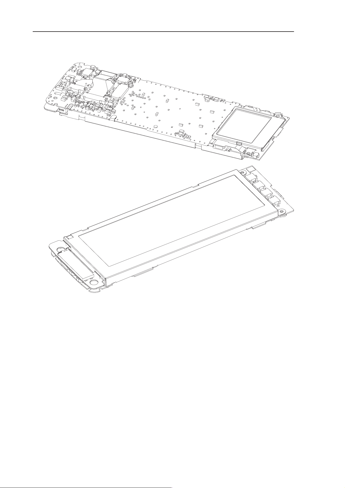
DL2 is located in the cover side of RAE–3. Figures below describe the two
sides of the module.
4. User Interfaces
Issue 1 06/01
Page 4 – 5
Page 6
RAE-3
PAMS
4. User Interfaces
Technical Documentation
Main Components
DL2 main components include UL2 PWB with components, PDA display and
CMT display.
Components on the module assembly include the following:
– Four layer, 0.6mm thick PWB (UL2) including:
Page 4 – 6
Figure 1. DL2 module
– PDA LCD CCFL backlight circuit.
– Power circuit for PDA LCD bias voltages.
– Power circuit and LEDs for CMT keypad and CMT display back-
light.
– Antenna clips and ground plane.
– Coaxial cable connector for antenna cable.
– 10–pin and 20–pin flex connectors for PDA display module.
Issue 1 06/01
Page 7

PAMS
RAE-3
Technical Documentation
– 50–pin flex connector for hinge flex.
– 10–pin flex connection for CMT display.
– 4–way stacker connection for piezo flex assembly.
– Pads for CMT keypad.
– PDA soft key switches.
– PDA LCD module including lightguide, piezo transformer FPC, CCFL and
metal frame.
– CMT Display module including metal frame and lightguide.
DC Characteristics
Supply voltages and power consumption are listed below:
Pin /
Conn.
X1/1,
X1/49,
X1/50
Line Sym-
bol
VB Battery Volt-
age
4. User Interfaces
Parameter Minimum T ypical Maximum Unit Notes
3.0 3.6 4.2 V 4.8V Absolute
maximum
210 mA
X1/1 1 VBB Logic voltage
2.7 2.8 2.9 V
20 mA
Connections
The 50–way FPC connects the DL2 to the BL8 (system logic and RF board) via
the hinge. It has all active signals for the DL2 module and supply pins. It is
connected to the 50–pin board–to–board connector X1.
DL2 has coaxial cable connector for antenna cable. This co–axial cable goes
through the hinge to the BL8 RF part.
X1 connector pinout
PIN/
Pins
1,49
50
11 VBB Logic voltage 2.7 2.8 2.9 V Supply
Line Sym-
bol
VB Battery voltage 3.0 3.6 4.2 V Supply
Parameter Min. T yp.
/
No
m.
Max. Unit Active
level
Function
3, 7,
19, 26,
37, 38,
44, 48
21 LCDPWR PDA LCD Volt-
GND Ground 0 V Supply
ages switch
Issue 1 06/01
0
1.58V
0.88V
VBB
V Inactive
Active
Page 4 – 7
Input. High
level turns
on supply
to display
Page 8

RAE-3
C
PAMS
4. User Interfaces
PIN/
Pins
16 GenSClk Serial Clock for
18 GenSDIO Serial Data for
46 Row5LCDCDCMT display con-
15 LCDEN CMT display en-
bol
MT display
CMT display
trol / data
able
Technical Documentation
Min.ParameterLine Sym-
/
No
m.
0 3.25 4.0 MHz Input
0
0.7xVBB
0
0.7xVBB
0
0.7xVBB
0
0.7xVBB
0.3xVBB
VBB
0.3xVBB
VBB
0.3xVBB
VBB
0.3xVBB
VBB
UnitMax.Typ.
level
V Low
High
V Low
High
V Control
Data
V Active
Inactive
FunctionActive
Input
Input
Input. Low
level selects command register
Input. Low
level enables writing to the
display
13 LCDRSTX CMT display reset 0
14 KBLIGHTS CMT keypad and
display backlight
control
22 LCDDa0 PDA display data 0
2 LCDDa1 PDA display data 0
4 LCDDa2 PDA display data 0
33 LCDDa3 PDA display data 0
8 LCDDa4 PDA display data 0
31 LCDDa5 PDA display data 0
32 LCDDa6 PDA display data 0
6 LCDDa7 PDA display data 0
0.7xVBB
0
0.7xVBB
1.58V
1.58V
1.58V
1.58V
1.58V
1.58V
1.58V
1.58V
0.3xVBB
VBB
0.3xVBB
VBB
0.88V
VBB
0.88V
VBB
0.88V
VBB
0.88V
VBB
0.88V
VBB
0.88V
VBB
0.88V
VBB
0.88V
VBB
V Active
Inactive
V Active
Inactive
V Low
High
V Low
High
V Low
High
V Low
High
V Low
High
V Low
High
V Low
High
V Low
High
Input. Low
level resets
the display
Input. High
level turns
lights on.
Input
Input
Input
Input
Input
Input
Input
Input
9 LCDDa8 PDA display data 0
1.58V
5 LCDDa9 PDA display data 0
1.58V
34 LCDDa10 PDA display data 0
1.58V
Page 4 – 8
0.88V
VBB
0.88V
VBB
0.88V
VBB
V Low
High
V Low
High
V Low
High
Issue 1 06/01
Input
Input
Input
Page 9

PAMS
RAE-3
Technical Documentation
PIN/
Pins
20 LCDDa11 PDA display data 0
25 DISPClk PDA display Pixel
35 LLClk PDA display Line
23 FSP PDA display
10 LCDM PDA display AC–
24 DISPON PDA display ON/
36 LCD_TEMPConnected to
30 Col0 Keypad column 0 0
27 Col1 Keypad column 1 0
28 Col2 Keypad column 2 0
43 Col3 Keypad column 3 0
45 Col4 Keypad column 4 0
29 Row0 Keypad row 0 0
39 Row1 Keypad row 1 0
40 Row2 Keypad row 2 0
41 Row3 Keypad row 3 0
bol
clock
pulse
Frame pulse
modulation
OFF
ground for color
display detection.
4. User Interfaces
Min.ParameterLine Sym-
/
No
m.
0.88V
1.58V
8 8.66 10 MHz
0
1.58V
0 10.8 12.5 kHz
0
1.58V
0 51.5 59 Hz
0
1.58V
0 10.8 15 kHz
0
1.58V
0
1.58V
0.7xVBB
0.7xVBB
0.7xVBB
0.7xVBB
0.7xVBB
0.7xVBB
0.7xVBB
0.7xVBB
0.7xVBB
VBB
0.88V
VBB
0.88V
VBB
0.88V
VBB
0.88V
VBB
0.88V
VBB
0.3xVBB
VBB
0.3xVBB
VBB
0.3xVBB
VBB
0.3xVBB
VBB
0.3xVBB
VBB
0.3xVBB
VBB
0.3xVBB
VBB
0.3xVBB
VBB
0.3xVBB
VBB
UnitMax.Typ.
V Low
V Low
V Low
V Low
V Low
V Active
V Low
V Low
V Low
V Low
V Low
V Low
V Low
V Low
V Low
FunctionActive
level
Input
High
Input
High
Input
High
Input
High
Input
High
Input
Inactive
Unused.
Input
High
Input
High
Input
High
Input
High
Input
High
Output
High
Output
High
Output
High
Output
High
Issue 1 06/01
Page 4 – 9
Page 10

RAE-3
PAMS
4. User Interfaces
PIN/
Pins
42 Row4 Keypad row 4 0
17 LCDPWM PDA LCD Con-
47 BACKPWM PDA LCD Back-
bol
trast control
light control
Antenna clip connector
DL2 has antenna clips that are connected to the antenna.
Min.ParameterLine Sym-
0.7xVBB
0
0.7xVBB
0
0.7xVBB
/
No
m.
50.7
335
Technical Documentation
UnitMax.Typ.
level
0.3xVBB
VBB
0.3xVBB
VBB
0.3xVBB
VBB
V Low
High
V
KHz
V
Hz
Low
High
Low
High
FunctionActive
Output
Input
Input
Pin Line
X1/1,
X1/49,
X1/50
Symbol
VB Battery
Parame-
ter
Voltage
Minimum Typical /
Nominal
3.0 3.6 4.2 V 4.8V Ab-
Maxi-
mum
Unit Notes
solute
maximum
X2 connector pinout
Row driver features a 10–pin flex connector.
Pin Line
Sym-
bol
1 GND 0 V LCD driving level for Y
2 XINH 0
3 YSCL 0
Minimum Typical / Nomi-
nal
Logic 0
0.8 x VDDY
0.9 x VDDY
Logic 1
Logic 0
Logic 1
Maximum Unit Notes
driver IC
0.2 x VDDY
VDDY
0.1 x VDDY
VDDY
V Line sub–sampling signal
for Y driver IC
V Shift clock for Y driver IC
4 FRY 0
0.8 x VDDY
5 VCCY
6 V5Y Low level supply voltage
7 NC Not connected
2.7 VCC–V5Y
Page 4 – 10
Logic 0
Logic 1
3.3
0.2 x VDDY
VDDY
4.5 V
V Output control for Y driver
IC
High level supply voltage
for Y driver IC
for Y driver IC
Issue 1 06/01
Page 11

PAMS
RAE-3
Technical Documentation
Pin
Sym-
bol
8 V0Y
9 VDD LCD driving level for Y
10 DY 0
MinimumLine
nal
8.0 V0Y–V5Y–VDD 33 V
0.8 x VDDY
Logic 0
Logic 1
0.2 x VDDY
VDDY
4. User Interfaces
NotesUnitMaximumTypical / Nomi-
LCD driving level for Y
driver IC
driver IC
Shift start pulse for Y driv-
er IC
X3 connector pinout
Column drivers feature a 20–pin flex connector.
Pin Line Symbol Minimum Typical / Nom-
inal
1 VCC V Logic supply for X driver
Maximum Unit Notes
2 VDDH V LCD supply for X driver
3 D23 0
0.7 x VDDX
4 D22 0
0.7 x VDDX
5 D21 0
0.7 x VDDX
6 D20 0
0.7 x VDDX
7 GCP 0
0.7 x VDDX
8 FR 0
0.7 x VDDX
9 LP 0
0.7 x VDDX
10 RES 0
0.7 x VDDX
11 D03 0
0.7 x VDDX
Logic 0
Logic 1
Logic 0
Logic 1
Logic 0
Logic 1
Logic 0
Logic 1
Logic 0
Logic 1
Logic 0
Logic 1
Logic 0
Logic 1
Logic 0
Logic 1
Logic 0
Logic 1
0.3 x VDDX
VDDX
0.3 x VDDX
VDDX
0.3 x VDDX
VDDX
0.3 x VDDX
VDDX
0.3 x VDDX
VDDX
0.3 x VDDX
VDDX
0.3 x VDDX
VDDX
0.3 x VDDX
VDDX
0.3 x VDDX
VDDX
V Digital video signal
V Digital video signal
V Digital video signal
V Digital video signal
V PWM width control
pulse for X driver
V Output alternation signal
for X drivers
V Data load and shift
pulse for X driver
V PWM counter reset sig-
nal for X driver
V Digital video signal
12 D02 0
13 D01 0
14 D00 0
Issue 1 06/01
0.7 x VDDX
0.7 x VDDX
0.7 x VDDX
Logic 0
Logic 1
Logic 0
Logic 1
Logic 0
Logic 1
0.3 x VDDX
VDDX
0.3 x VDDX
VDDX
0.3 x VDDX
VDDX
V Digital video signal
V Digital video signal
V Digital video signal
Page 4 – 11
Page 12

RAE-3
PAMS
4. User Interfaces
MinimumLine SymbolPin
inal
15 XSCL 0
0.7 x VDDX
16 D13 0
0.7 x VDDX
17 D12 0
0.7 x VDDX
18 D11 0
0.7 x VDDX
19 D10 0
0.7 x VDDX
20 GND 0 V Logic Low signal for X
Logic 0
Logic 1
Logic 0
Logic 1
Logic 0
Logic 1
Logic 0
Logic 1
Logic 0
Logic 1
0.3 x VDDX
VDDX
0.3 x VDDX
VDDX
0.3 x VDDX
VDDX
0.3 x VDDX
VDDX
0.3 x VDDX
VDDX
Technical Documentation
NotesUnitMaximumTypical / Nom-
V Shift clock for X driver
V Digital video signal
V Digital video signal
V Digital video signal
V Digital video signal
driver,
LCD low level for X driver
X6 connector pinout
X6 is a 4 way ’stacker’ connector to piezo FPC.
Pin Line Sym-
bol
1 Feedback Feedback from CCFL
2 Piezo_in Input to primary of pie-
3 AGND 0 V Supply
4 GND 0 V Supply
Parameter Mini-
output
zo transformer
T ypical
mum
0 0.84 1.54 V Input
0 5 8 Vrms Output
/ Nomi-
nal
Maxi-
mum
Unit Function
X7 connector pinout
X7 is a 10 way flex connector to CMT LCD..
Pin Line Sym-
bol
1 GND Ground 0 V Supply
2 VOUT DC/DC voltage con-
3 LCDRSTX Reset 0 0.3xVBB Active Output
Parameter Mini-
verter output
mum
T ypical
/ Nomi-
nal
Maxi-
mum
9
Unit Notes Function
Input
4,5 VBB Supply voltage 2.7 2.8 2.9 V Supply
300 uA
6 GenSClk Serial clock input 203kHz 3.25MHz3.25MHz MHz Output
Page 4 – 12
Issue 1 06/01
Page 13

PAMS
RAE-3
Technical Documentation
Pin
bol
6 0
7 GenSDIO Serial data input 0 0.3xVBB V Low Output
8 Row5LCDCDControl/display data
9 LCDEN Chip select input 0 0.3xVBB Active Output
10 OSC* External clock for
ParameterLine Sym-
flag input
LCD
Minimum
0,7xVBB
0.7xVBB VBB V High
0 0.3xVBB Control Output
0.7xVBB VBB Data
0.7xVBB VBB Inactive
Typical
/ Nomi-
nal
mum
0.3xVBB
VBB
4. User Interfaces
V Low
High
Connected to
VBB on UL2
FunctionNotesUnitMaxi-
Output
Inactive
RF connection
Pin Line
symbol
RF Antenna feed
Parameter Minimum
frequency
890 MHz 1880 MHz 33 dBm (peak)
cable
Maximum
frequency
Maximum power Notes
28.8 dBm (average)
Issue 1 06/01
Page 4 – 13
Page 14

RAE-3
PAMS
4. User Interfaces
Functional description
Power distribution and control signals
The following block diagram describes the distribution of power supplies within
DL2.
Battery voltage VB is fed directly to the illumination LEDS (CMT keymat and
CMT display)
The regulated band supply VBB generated on the BL8 module supplies the
CMT display, control logic and PDA display supply.
A power switch is used to remove the voltage supply from the control logic and
PDA display when the display is turned off.
Technical Documentation
VB
VBB
LCDPWR
GND
110mA 20mA typ 10mA typ
typical
300uA max
16mA typ
PDA LCD Bias power
and control logic
Figure 2. Power distribution and control signals of UL2.
CMT
LCD
PDA LCD
backlight
KBLIGHTSBACKPWM
Keyboard
backlight backlight
CMT LCD
Page 4 – 14
Issue 1 06/01
Page 15

PAMS
RAE-3
Technical Documentation
DL2 Circuit Description
The module is connected via a 50 way FPC to the BL8 system logic.
The module includes following main blocks:
– CMT keyboard geometries.
– Switches for PDA soft keyboard
– Backlight LEDs for CMT keypad and CMT LCD illumination.
– CMT LCD.
– PDA LCD module.
– PDA LCD backlight circuit.
– PDA LCD power circuit.
– PDA LCD interface control logic.
4. User Interfaces
– Hinge flex connector.
– Antenna connector and ground plane.
Keypad scanning.
There is 26 keys located in DL2 module. 6 PDA soft keys are located inside the
lid and 20 CMT keys on the outer side. All these keys are in the same keyboard
matrix as the QWERTY–keypad in the UL8 module.
Col(0–4) are used as column lines in keypad. Row(0–4 and 6) are used as row
lines.
When a key is pressed the MCU gets an interrupt from a row and starts scanning. One column at a time is written low and rows are used to read which key
is pressed.
CMT keypad and CMT LCD backlight
The CMT keypad and CMT display are illuminated with LEDs. Each LED is
driven by a separate drive transistor.
LEDs for CMT display are driven with appoximately 5mA each.
LEDs for CMT keymat illumination are driven with approximately 2.5mA each.
CMT LCD
Mechanical structure
LCD includes the frame, LCD cell with driver chip, reflector, adhesive tapes,
and lightguide. The LCD is electrically connected to the UL2 PWB with a FPC
and board–to–board connector.
Issue 1 06/01
Page 4 – 15
Page 16

RAE-3
PAMS
4. User Interfaces
The frame includes clips to mechanically attach the display to the UL2 PWB
and also keep LCD cell and lightguide in place.
LCD cell specification
The LCD cell includes the display driver.
PDA LCD Module .
PDA LCD circuit main blocks are LCD glass including drivers, PDA LCD bias
voltage power circuit and a control IC.
Display resolution 640 (x3) x 200 dots
Active area 107.52 x 33.6
Dot pitch 0.168 x 0.168mm
Display mode D–TFD, Color, Transmissive
Frame frequency 51.5 Hz typical
Technical Documentation
Parameter Function
Colors 4096 colors, 12–bit RGB
Display brightness 100nit (full brightness typical)
PDA LCD Backlight circuit
VB
VBB
BACKPWM
Control
DISPON
circuit
Driver
Piezo
transformer
CCFL
The control circuit generates a square wave input to the piezo driver circuit.
This signal is maintained at the resonant frequency of the piezo transformer.
The driver is based around 2 FETs in Push–pull configuration. There is a single
coil between the FETs and the piezo transformer.
Both FETs are turned off while the CCFL is off during dimming (BACKPWM
low).
Page 4 – 16
Figure 3. Backlight Power Supply
Issue 1 06/01
Page 17

PAMS
RAE-3
Technical Documentation
The piezo transformer part is soldered onto a FPC with the CCFL.
Piezo transformer characteristic Value
Input voltage 8Vrms Max
Output power 1 W max
Output voltage 200 Vrms min
Output current 4.5mA
Operating current 1.5mA nominal
Operating frequency 130 +/– 10 kHz
The CCFL lamp is 2.6mm outer diameter and 1.8 mm inner diameter Double
tube.
CCFL lamp characteristic Value
Operating frequency 150 kHz (typ.)
Starting Voltage About 500 Vrms
4. User Interfaces
Operating Voltage 200 Vrms
Tube current 1 mA min , 3mA max
Operating current 1.5mA
PDA LCD Power circuit
PDA LCD power circuit generates the bias voltages necessary for the PDA display panel. Block diagram below.
VCC
Flyback Regulator
LCDPWM
Data
Control ASIC
Synchronisation
Swing Mode
Regulator
DY
V0Y
V5Y
VCCY
FRY
YSCL
Issue 1 06/01
XINH
Figure 4. Block diagram of PDA Power Supply
Page 4 – 17
Page 18

RAE-3
PAMS
4. User Interfaces
The flyback regulator generates a negative bias voltage (Nominally –12V) from
the battery voltage. The output of the flyback generator is temperature compensated and adjusted under software control.
The control ASIC handles the refresh of data to the PDA display panel and the
generation of synchronisation signals for the swing mode regulator.
Antenna connectors and ground plane
The RF–signal from the external antenna connector/switch on BL8 is fed to the
antenna via a coaxial cable that is led through the hinge. The signal is fed to
the antenna through a coaxial connector and an antenna clip which are placed
on the UL2 PWB.
The UL2 PWB includes the separate ground area that is required by the antenna.
Technical Documentation
Page 4 – 18
Issue 1 06/01
Page 19

PAMS
RAE-3
Technical Documentation
QWERTY Keyboard Module UL8
General
UL8 is the combined QWERTY keypad/flex connection module. The base flex
is single–sided, so all the components are on the same side of the flex.
Approximate component placement is shown below:
4. User Interfaces
70 pin connector 5469145
50 pin connector 5469817
Figure 5. Component placement
AF8 PWB
Issue 1 06/01
Page 4 – 19
Page 20

RAE-3
PAMS
4. User Interfaces
AF8 PWB
AF8 is a small additional PWB to achieve ”bulls eye” shaped pads for the earpiece and connection for the battery removal switch. (Check that the RAE-3
software supports the battery removal switch feature.)
The approximate shape of AF8 is shown below.
One 22pF SMD capacitor is assembled to the AF8.
Technical Documentation
Page 4 – 20
Figure 6. AF8 PWB
Issue 1 06/01
 Loading...