

Page 1

PAMS Technical Documentation
RAE-3 Series PDA
3. RF+System Module BL8
issue 1 06/01
Copyright 2001. Nokia Mobile Phones. All Rights Reserved.
Page 2
RAE-3
PAMS
3. RF+System Module BL8
AMENDMENT RECORD SHEET
Amendment
Number
Date Inserted By Comments
06/01 OJuntunen
Technical Documentation
Page 3 – 2
issue 1 06/01
Page 3

PAMS
RAE-3
Technical Documentation
CONTENTS –Troubleshooting
Abbreviations 3 – 6. . . . . . . . . . . . . . . . . . . . . . . . . . . . . . . . . . . . . . . .
RAE-3 Structure 3 – 9. . . . . . . . . . . . . . . . . . . . . . . . . . . . . . . . . . . . . . . .
RAE-3 Modules 3 – 9. . . . . . . . . . . . . . . . . . . . . . . . . . . . . . . . . . . . . . . . .
List of Modules 3 – 9. . . . . . . . . . . . . . . . . . . . . . . . . . . . . . . . . . . .
Technical Summary of System Part 3 – 10. . . . . . . . . . . . . . . . . . . . .
Block Diagram 3 – 11. . . . . . . . . . . . . . . . . . . . . . . . . . . . . . . . . . . . . . .
Electrical Characteristics 3 – 12. . . . . . . . . . . . . . . . . . . . . . . . . . . . . . . . .
Power Supply 3 – 12. . . . . . . . . . . . . . . . . . . . . . . . . . . . . . . . . . . . . . . .
System Connector 3 – 13. . . . . . . . . . . . . . . . . . . . . . . . . . . . . . . . . . . .
Battery Connector 3 – 14. . . . . . . . . . . . . . . . . . . . . . . . . . . . . . . . . . . .
Backup battery connector 3 – 15. . . . . . . . . . . . . . . . . . . . . . . . . . . . . .
SIM card connector 3 – 15. . . . . . . . . . . . . . . . . . . . . . . . . . . . . . . . . . .
MMC Connector 3 – 16. . . . . . . . . . . . . . . . . . . . . . . . . . . . . . . . . . . . . .
Infrared interface 3 – 17. . . . . . . . . . . . . . . . . . . . . . . . . . . . . . . . . . . . .
UI Signals 3 – 17. . . . . . . . . . . . . . . . . . . . . . . . . . . . . . . . . . . . . . . . . . .
System – RF interface 3 – 21. . . . . . . . . . . . . . . . . . . . . . . . . . . . . . . .
3. RF+System Module BL8
Page No
Functional Description 3 – 25. . . . . . . . . . . . . . . . . . . . . . . . . . . . . . . . . . .
Modes of Operation 3 – 25. . . . . . . . . . . . . . . . . . . . . . . . . . . . . . . . . . .
Clocking Scheme 3 – 25. . . . . . . . . . . . . . . . . . . . . . . . . . . . . . . . . . . . .
Power Control and Reset 3 – 26. . . . . . . . . . . . . . . . . . . . . . . . . . . . . .
Power Distribution 3 – 26. . . . . . . . . . . . . . . . . . . . . . . . . . . . . . . . . .
Power up 3 – 28. . . . . . . . . . . . . . . . . . . . . . . . . . . . . . . . . . . . . . . . .
Power Off 3 – 28. . . . . . . . . . . . . . . . . . . . . . . . . . . . . . . . . . . . . . . . .
Charging 3 – 28. . . . . . . . . . . . . . . . . . . . . . . . . . . . . . . . . . . . . . . . . .
Resets and Watchdogs 3 – 29. . . . . . . . . . . . . . . . . . . . . . . . . . . . .
System to interface 3 – 31. . . . . . . . . . . . . . . . . . . . . . . . . . . . . . . . . . .
CPU block 3 – 31. . . . . . . . . . . . . . . . . . . . . . . . . . . . . . . . . . . . . . . . . . .
MEMORIES block 3 – 31. . . . . . . . . . . . . . . . . . . . . . . . . . . . . . . . . . . .
XIP Memories 3 – 31. . . . . . . . . . . . . . . . . . . . . . . . . . . . . . . . . . . . .
SDRAM Memory 3 – 32. . . . . . . . . . . . . . . . . . . . . . . . . . . . . . . . . . .
Serial Flash Memory 3 – 32. . . . . . . . . . . . . . . . . . . . . . . . . . . . . . . .
MMC block 3 – 33. . . . . . . . . . . . . . . . . . . . . . . . . . . . . . . . . . . . . . . . . .
IRDA block 3 – 33. . . . . . . . . . . . . . . . . . . . . . . . . . . . . . . . . . . . . . . . . .
UI block 3 – 33. . . . . . . . . . . . . . . . . . . . . . . . . . . . . . . . . . . . . . . . . . . . .
Phone LCD Interface 3 – 33. . . . . . . . . . . . . . . . . . . . . . . . . . . . . . .
Keyboard Interface 3 – 33. . . . . . . . . . . . . . . . . . . . . . . . . . . . . . . . .
Earpiece and HF Speaker lines 3 – 34. . . . . . . . . . . . . . . . . . . . . .
Battery removal signal 3 – 34. . . . . . . . . . . . . . . . . . . . . . . . . . . . . .
SYSCON block 3 – 34. . . . . . . . . . . . . . . . . . . . . . . . . . . . . . . . . . . . . . .
Serial connections 3 – 35. . . . . . . . . . . . . . . . . . . . . . . . . . . . . . . . . .
issue 1 06/01
Page 3 – 3
Page 4

RAE-3
PAMS
3. RF+System Module BL8
External Audio Interface 3 – 35. . . . . . . . . . . . . . . . . . . . . . . . . . . . .
Charger Interface 3 – 36. . . . . . . . . . . . . . . . . . . . . . . . . . . . . . . . . .
External RF 3 – 36. . . . . . . . . . . . . . . . . . . . . . . . . . . . . . . . . . . . . . .
POWER block 3 – 36. . . . . . . . . . . . . . . . . . . . . . . . . . . . . . . . . . . . . . . .
Use of CCONT ADC channels 3 – 37. . . . . . . . . . . . . . . . . . . . . . .
AUDIO_RFI block 3 – 38. . . . . . . . . . . . . . . . . . . . . . . . . . . . . . . . . . . .
RFI 3 – 38. . . . . . . . . . . . . . . . . . . . . . . . . . . . . . . . . . . . . . . . . . . . . . .
Audio 3 – 38. . . . . . . . . . . . . . . . . . . . . . . . . . . . . . . . . . . . . . . . . . . . .
Introduction to RF of BL8 3 – 40. . . . . . . . . . . . . . . . . . . . . . . . . . . . . . . .
Maximum ratings 3 – 40. . . . . . . . . . . . . . . . . . . . . . . . . . . . . . . . . . . . .
RF frequency plan 3 – 40. . . . . . . . . . . . . . . . . . . . . . . . . . . . . . . . . . . .
DC characteristics 3 – 41. . . . . . . . . . . . . . . . . . . . . . . . . . . . . . . . . . . .
Regulators 3 – 41. . . . . . . . . . . . . . . . . . . . . . . . . . . . . . . . . . . . . . . .
Control signals 3 – 41. . . . . . . . . . . . . . . . . . . . . . . . . . . . . . . . . . . . .
4.7 V regulator in VCP line 3 – 42. . . . . . . . . . . . . . . . . . . . . . . . . .
Power distribution diagram 3 – 43. . . . . . . . . . . . . . . . . . . . . . . . . .
Technical Documentation
RF characteristics 3 – 44. . . . . . . . . . . . . . . . . . . . . . . . . . . . . . . . . . . . . . .
Transmitter characteristics 3 – 44. . . . . . . . . . . . . . . . . . . . . . . . . . .
Receiver characteristics 3 – 45. . . . . . . . . . . . . . . . . . . . . . . . . . . . .
Functional descriptions 3 – 46. . . . . . . . . . . . . . . . . . . . . . . . . . . . . . . . . .
RF block diagram 3 – 46. . . . . . . . . . . . . . . . . . . . . . . . . . . . . . . . . . . . .
Frequency synthesizer 3 – 48. . . . . . . . . . . . . . . . . . . . . . . . . . . . . . . .
Receiver 3 – 48. . . . . . . . . . . . . . . . . . . . . . . . . . . . . . . . . . . . . . . . . . . .
Transmitter 3 – 48. . . . . . . . . . . . . . . . . . . . . . . . . . . . . . . . . . . . . . . . . .
AGC strategy 3 – 49. . . . . . . . . . . . . . . . . . . . . . . . . . . . . . . . . . . . . . . .
AFC function 3 – 49. . . . . . . . . . . . . . . . . . . . . . . . . . . . . . . . . . . . . . . . .
Antenna switch 3 – 50. . . . . . . . . . . . . . . . . . . . . . . . . . . . . . . . . . . . . . .
SWITCH (SW_1, SW_2) 3 – 50. . . . . . . . . . . . . . . . . . . . . . . . . . . .
TX–FILTERS 3 – 50. . . . . . . . . . . . . . . . . . . . . . . . . . . . . . . . . . . . . .
RX–FILTERS 3 – 50. . . . . . . . . . . . . . . . . . . . . . . . . . . . . . . . . . . . . .
Receiver blocks 3 – 51. . . . . . . . . . . . . . . . . . . . . . . . . . . . . . . . . . . . . .
RX EGSM900/DCS1800 DUALBAND SAW FILTER 3 – 51. . . .
EGSM Pre–amplifier (LNA) 3 – 51. . . . . . . . . . . . . . . . . . . . . . . . . .
DCS1800 Pre–amplifier (LNA) 3 – 52. . . . . . . . . . . . . . . . . . . . . . .
GSM/PCN IC (Hagar), RX part 3 – 52. . . . . . . . . . . . . . . . . . . . . . .
Transmitter blocks 3 – 53. . . . . . . . . . . . . . . . . . . . . . . . . . . . . . . . . . . .
IQ–modulator and TX–AGC in HAGAR IC 3 – 53. . . . . . . . . . . . .
EGSM TX saw filter 725057 3 – 53. . . . . . . . . . . . . . . . . . . . . . . . .
Diplexer 3 – 54. . . . . . . . . . . . . . . . . . . . . . . . . . . . . . . . . . . . . . . . . . .
TX–buffer and 3dB attenuator 3 – 54. . . . . . . . . . . . . . . . . . . . . . . .
Dual–band power amplifier 3 – 54. . . . . . . . . . . . . . . . . . . . . . . . . .
Directional coupler 3 – 55. . . . . . . . . . . . . . . . . . . . . . . . . . . . . . . . .
Power detector 3 – 56. . . . . . . . . . . . . . . . . . . . . . . . . . . . . . . . . . . .
Synthesizer blocks 3 – 56. . . . . . . . . . . . . . . . . . . . . . . . . . . . . . . . . . . .
Page 3 – 4
issue 1 06/01
Page 5

PAMS
RAE-3
Technical Documentation
VCTCXO, reference oscillator 3 – 56. . . . . . . . . . . . . . . . . . . . . . . .
SHF PLL in HAGAR 3 – 56. . . . . . . . . . . . . . . . . . . . . . . . . . . . . . . .
VCO module 3 – 57. . . . . . . . . . . . . . . . . . . . . . . . . . . . . . . . . . . . . .
Connections 3 – 58. . . . . . . . . . . . . . . . . . . . . . . . . . . . . . . . . . . . . . . . . . . .
Antenna 3 – 58. . . . . . . . . . . . . . . . . . . . . . . . . . . . . . . . . . . . . . . . . . . . .
RF connector and antenna switch 3 – 58. . . . . . . . . . . . . . . . . . . . . .
RF–System interface 3 – 58. . . . . . . . . . . . . . . . . . . . . . . . . . . . . . . . . .
Timings 3 – 62. . . . . . . . . . . . . . . . . . . . . . . . . . . . . . . . . . . . . . . . . . . . . . . .
Transmit power Timing 3 – 62. . . . . . . . . . . . . . . . . . . . . . . . . . . . . . .
Synthesizer clocking 3 – 62. . . . . . . . . . . . . . . . . . . . . . . . . . . . . . . . . .
3. RF+System Module BL8
issue 1 06/01
Page 3 – 5
Page 6

RAE-3
PAMS
3. RF+System Module BL8
Abbreviations
ACCIF ACCessory InterFace block of MADLinda
A/D Analog–to–Digital
ADC Analog–to–Digital Converter
AFC Automatic Frequency Control
AGC Automatic Gain Control
AMM ARM MegaModule
API ARM Port Interface in LMM
ARM Advanced RISC Machines
ASIC Application Specific Integrated Circuit
AVG Average
BB Baseband
BGA Ball Grid Array package
bl8 RAE-3 System/RF module
BLL–3 Litium–Ion battery back for RAE-3
CCONT Multifunction power management IC for DCT3
CCR Clock Configuration Register in MADLinda
CHAPS DCT3 Charging control ASIC – used in bl8 system HW
CMT Cellular Mobile Transceiver
COBBA DCT3 RF–interface and Audio codec IC
COBBA_GJP Serial control interface version of COBBA
CRFU3 UHF RF IC – used in bl8 RF HW
CSD Card–specific Data, register in MultiMediaCards
CSP Chip Scale Package
CTSI Clocking, Timing, Sleep & Interrupt block of MADLinda
D/A Digital–to–Analog
DAC Digital–to–Analog Converter
DCD Data Carrier Detect
DCE Data Communication Equipment
DCT3 3rd generation Digital Core Technology
DNL Differential non–linearity
DMA Direct Memory Access
DL2 RAE–3 Color UI module
DSP Digital Signal Processor
DTMF Dual Tone Multi Frequency
DTR Data Terminal Ready
EAD External Accessory Detect
EMC Electromagnetic Compatibility
EMI Electromagnetic Interference
ESD Electrostatic Discharge
FBUS Full Duplex Serial Bus in NOKIA’s phones
FFS Flash File System
GPIO General Purpose Input/Output (block in MADLinda)
Technical Documentation
– used in bl8 system HW
– used in bl8 system HW
Page 3 – 6
issue 1 06/01
Page 7

PAMS
RAE-3
Technical Documentation
HAGAR Direct conversion RF ASIC – used in bl8 RF HW
HF Hands Free
HSCSD High Speed Circuits Switched Data
HW Hardware
IC Integrated Circuit
ICE In–Circuit Emulator
INL Integral non–linearity
IO Input/Output
IR Infrared
IrDA Infrared Data Association
JTAG Joint Test Action Group, commonly used as a synonym
LCD Liquid Crystal Display
LEAD Low power Enhanced Architecture DSP
LEAD2 Digital Signal Processor block of MADLinda
LMM LEAD2 MegaModule – DSP module in MADLinda
MAD MCU+ASIC+DSP chip (MCU–ASIC–DSP)
MAD2 GSM version of MAD
MAD2PR1 A pin reduction version of the MAD2
MAD2WD1 High Speed Data version of MAD2 by Wireless Data
MADLinda MAD based version of RAE-3 Communicator ASIC
MBUS 1–wire half duplex serial bus in NOKIA’s phones
MCU Micro Controller Unit
MFI Modulator and filter interface in MAD2
MMC MultiMediaCard
MMU Memory Management Unit
MPU Micro Processor Unit
NTC Negative Temperature Coefficient (resistor)
PCI Phone Control Interface
PCM Pulse Code Modulation
PCR Pin Configuration Register in MADLinda
PDA Personal Digital Assistant
PHF Personal Hands Free
PLL Phase Locked Loop
PMM Permanent Memory Management block (Plato UI)
PPM Post Programmable Memory
PUP PIO, USART and PWM block of MADLinda
PWB Printed Wiring Board
PWM Pulse Width Modulation
R&D Research and development
RAM Random Access Memory
RF Radio Frequency
RFI RF Interface
ROM Read Only Memory
RTC Real Time Clock
SCU Synthesizer Control Unit
3. RF+System Module BL8
for boundary scan (IEEE 1149.1) testing
– in text refers to MADLinda’s ARM9 processor
issue 1 06/01
Page 3 – 7
Page 8

RAE-3
PAMS
3. RF+System Module BL8
SCR System Configuration Register in MADLinda
SDRAM Synchronous Dynamic RAM
SIM Subscriber Identify Module
SIMIF Subscriber Identify Module Interface
SIR Serial Infrared (speed 115.2kbit/s)
SPI Serial Peripheral Interface
Spock Second generation communicator RAE–2
SSR System Status Register in MADLinda
SUMMA VHF RF IC – used in bl8 RF HW
SW Software
TAP Test Access Port (Boundary Scan)
TI Texas Instruments
TVS Transient Voltage Suppressor
UART Universal Asynchronous Receiver Transmitter
USART Universal Synchronous/Asynchronous Receiver
Transmitter
UI User Interface
UI1 RAE-3 Black&White UI module
VCTCXO Voltage Controlled Temperature Compensated Oscillator
VCXO Voltage Controlled Oscillator
VIA Versatile Interconnection Architecture (inside MADLinda)
WD1 Wireless Data Engine 1
XIP Execute In Place (memory)
(TBC) (To be checked)
(TBD) (To be defined)
Technical Documentation
Page 3 – 8
issue 1 06/01
Page 9
PAMS
RAE-3
Technical Documentation
RAE-3 Structure
This document specifies the system HW part of RAE–3 GSM900/GSM1800
Dual Band Communicator. The BL8 module contains both the system hardware and the RF components. The system part of the BL8 module functions as
a combined CMT baseband and PDA engine.
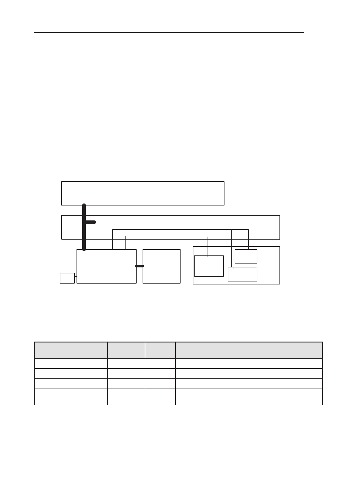
RAE-3 Modules
DL2 – Color UI module
3. RF+System Module BL8
UL8 QWERTY –flex module
Audio
holder
MIC
BL8
SYSTEM/RF
module
Lithium
Battery
BLL–3
(Li–Ion)
Figure 1. RAE–3 modules
Battery
removal
switch
Ear–
piece
HF
speaker
List of Modules
Table 1. List of submodules
Name of module Type code Material
code
RF&System BL8 0201278 GSM phone + PDA module, European FLASH mem
User Interface DL2 0201282 PDA + CMT displays, Colour LCD
Keyboard and Hinge flex UL8 0201667 Audio PWB and connectors
MRAE3 0261997 Mechanical assembly parts , no language dependent
parts
Notes
issue 1 06/01
Page 3 – 9
Page 10

RAE-3
PAMS
3. RF+System Module BL8
Technical Summary of System Part
The RAE-3 system hardware is based on a special version of the DCT3 MAD2
ASIC called MADLinda. MADLinda carries out all the signal processing and operation controlling tasks of the phone as well as all PDA tasks. To be able to run
simultaneously both CMT and PDA applications, MADLinda (ROM1) has a
52MHz ARM9 core.
MADLinda’s main blocks include: ARM925 MPU Subsystem, Traffic Controller
(TC), LEAD2 DSP megamodule (LMM), GSM System Logic and PDA peripherals. ARM925 MPU Subsystem includes ARM9TDMI core, data and instruction
caches, data and instruction memory management units (MMU) and write and
address buffers. Traffic Controller includes primary DMA controller, LCD controller and Flash and SDRAM memory interfaces. The System Logic of MAD2 is
able to support high speed data features (HSCSD). PDA peripherals include
interfaces for Serial Flash, MMC, IrDA, serial port, IOs and PWMs.
In addition of the MADLinda IC the system hardware includes memories, infrared transceiver, COBBA_GJP, CCONT and CHAPS ASICs, audio amplifier
and power regulators. CSP packages are used for all ASICs. System HW also
has connectors for MultiMediaCard (MMC) and SIM card, UI connector and
pads for system connector’s spring contacts.
Technical Documentation
Three XIP Flash devices are used for program code storage. A serial Flash device is used half for the Flash file system and half to save application code. A
synchronous DRAM (SDRAM) device is used as data memory. Code can also
be run from the SDRAM. This is used to run applications loaded from Serial
Flash or MultiMediaCard.
The main battery voltage range in RAE-3 is 3.0V to 4.2V. Battery charging is
controlled in SW using CCONT and CHAPS ASICs. RAE-3 can also supply 3
V(max 100mA) accessory voltage out from system connector.
The system electronics run from a 2.8V power rail. 1.8V is used as core voltage
inside MADLinda and as I/O voltage for XIP Flash memory interface.
Power supplying of the BL8 module, both system HW and RF, and also 2.8V
supplying for the UI module is carried out in system HW. A linear regulator is
used to generate 2.8V VBB voltage and a DC/DC converter is used to generate
the 1.8V Vcore voltage. Accessory voltage and MMC supply are generated with
separate 3V linear regulators. Other supplies are generated using the CCONT
power ASIC (4.7V needed in DCT4 RF is generated in RF side). CCONT generates also the main reset for the system.
Both 3V and 5V Plug–in SIM–cards are supported. SIM is interfaced through
CCONT, which does signal level shifting and generates correct supply voltage
for SIM.
A real time clock function is integrated into CCONT, which utilizes the same
32kHz clock supply as the sleep clock. A rechargeable backup battery provides
backup power to run the RTC when the main battery is removed. The backup
time is about 10 days. Note also the information in section 8 chapter 2.6.
Page 3 – 10
issue 1 06/01
Page 11
PAMS
RAE-3
Technical Documentation
The interface from the system part and the RF and audio sections is handled
by a specific ASIC COBBA_GJP. This ASIC provides A/D and D/A conversion
of the in–phase and quadrature receive and transmit signal paths and also A/D
and D/A conversions of received and transmitted audio signals. Data transmission between the COBBA_GJP and the MADLinda is implemented using serial
connections. Digital speech processing is executed by the MADLinda ASIC.
External audio is connected to RAE-3 through system connector’s XMIC and
XEAR lines.
Serial connection channels in RAE-3 include IrDA, MBUS, and serial port.
MBUS and serial port have logic level signals which are connected through system connector. IR transceiver is next to the system connector at the bottom end
of RAE-3 device.
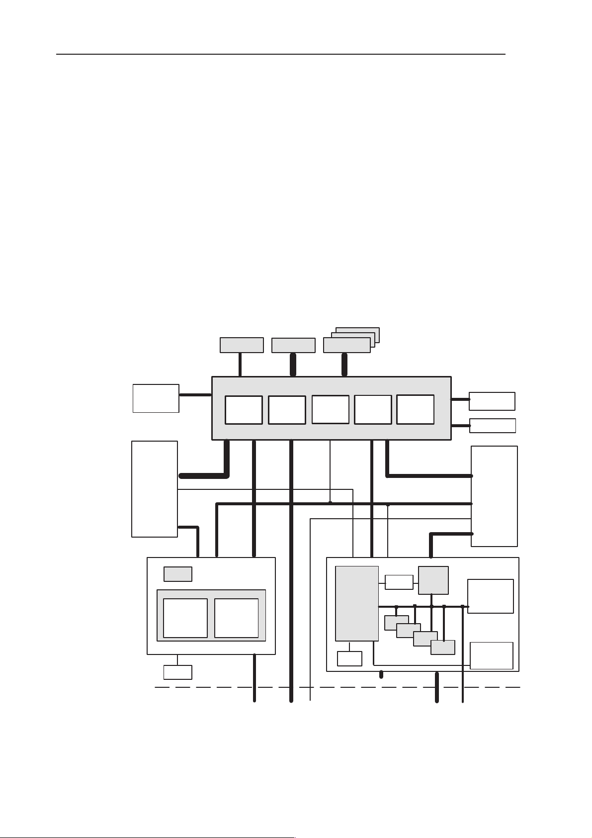
Block Diagram
SERIALFLASH
SDRAM
XIP MEMORIES
FLASH
3. RF+System Module BL8
MULTI
MEDIA
CARD
CONNECTOR
UI
CONNECTOR
UI SIGNALS
AUDIO
(EARP,
SPEAKER)
AUDIO
AMP
PCM
CODEC
MIC
COBBA
PDA
PERIPHERALS
_GJP
AUDIO
MADLINDA
_RFI
RFI
ARM925
MPU
SUBSYSTEM
TRAFFIC
CONTROLLER
32
CCONT
KHZ
XTAL
SYSTEM
LOGIC
ACK UP
B
BATTERY
VBB
REG.
SYSTEM SUPPLIES
LMM
(DSP)
VCORE
REG.
CHAPS
VMMC
REG.
ACCPWR
REG.
HALL
SENSOR
IRDA
SYSTEM
CONNECTOR
SERIAL
INTERFACES
EXTERNAL
AUDIO
EXTERNAL
RF
CHARGER
POWER
BATTERY
CONNECTOR
SIM
CARD
CONNECTOR
SYS
issue 1 06/01
RF SIGNALS
Figure 2. RAE-3 SYSTEM PART BLOCK DIAGRAM
RF SUPPLIES
RF
Page 3 – 11
Page 12
RAE-3
PAMS
3. RF+System Module BL8
Technical Documentation
Electrical Characteristics
Power Supply
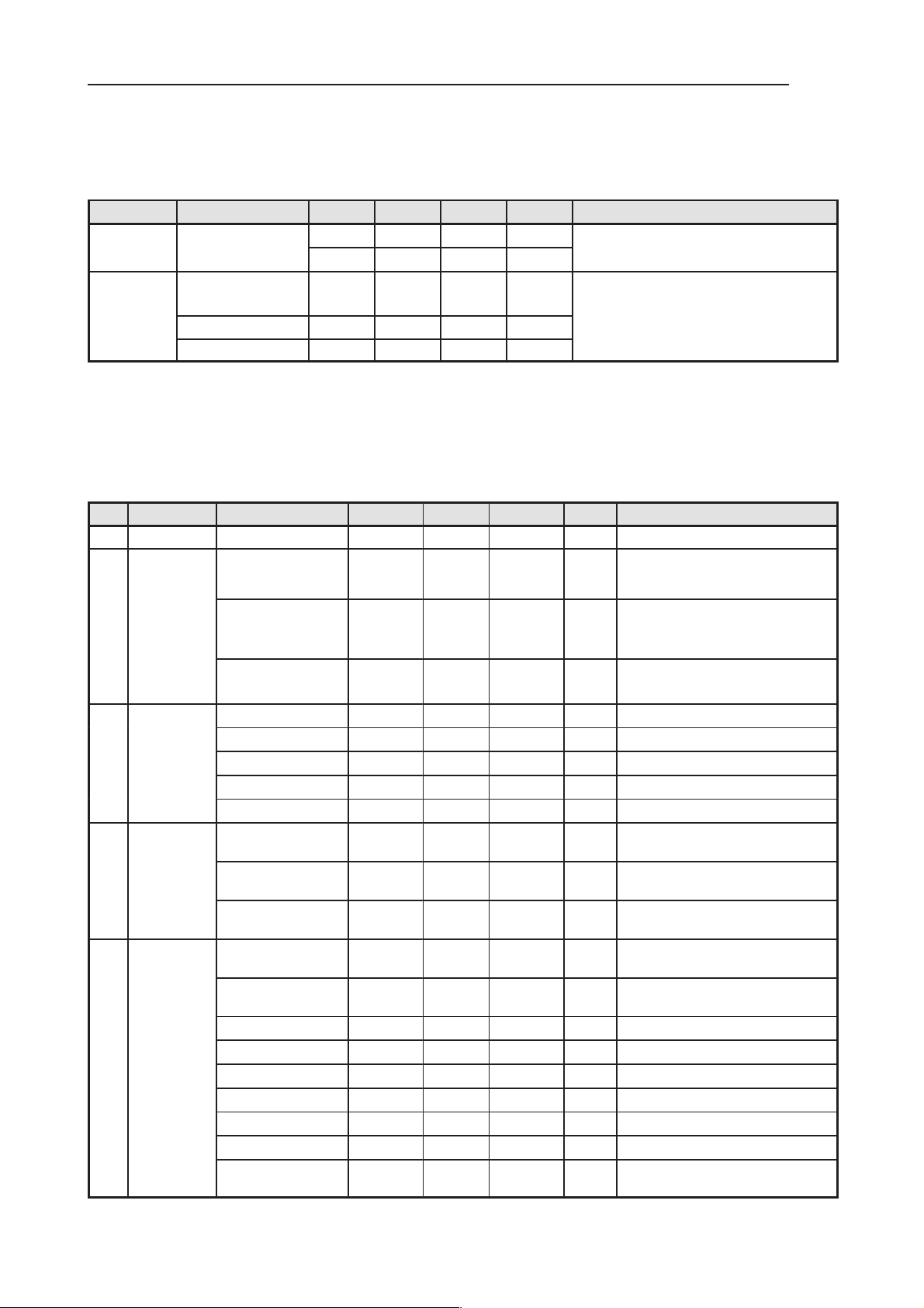
Table 2. Operating voltages and power consumptions
Name Parameter Min Typ Max Unit Notes
VIN Voltage 3.4 18 V Charging voltage
VBATT Voltage 3.0 3.6 4.8 V Voltage directly from main battery –to Vcore
450 mA typical for whole bl8
VB Voltage 3.0 3.6 4.8 V Filtered battery voltage
VB_CCONT Voltage 3.0 3.6 4.8 V Filtered battery voltage
VBB Voltage
Current
FLVPP Voltage
2.74 2.8 2.86 V System HW supply voltage,
45 400 mA typ. measured, max available from regulator
0 2.8 V Connected to MADLinda IO in assembled de-
req. and RF part,
– to VBB req. and to UI
– to CCONT and audio HF amplifier
vise. Functions as program enable in 2.8V .
Current
Vcore Voltage
Current
VMMC Voltage
Current
VACC Voltage
Current
VSIM Voltage 4.8 5.0 5.2 V Voltage to SIM, 5V selected
Current 3 10 30 mA 2)
Voltage
Current
VCOBBA Voltage
Current
VXO Voltage
Current
VRX Voltage
Current
VSYN_1 Voltage
Current
VSYN_2 Voltage
Current
VTX Voltage
Current
1.7 1.8 1.9 V Core voltage
2.74 3.0 3.1 V MMC supply voltage
3.03 3.3 3.4 V Accessory supply voltage output
2.8 3.0 3.2 V Voltage to SIM, 3V selected
1 6 30 mA 2)
2.7 2.8 2.85 V COBBA_GJP analog supply (CCONT VR6)
2.7 2.8 2.85 V
2.7 2.8 2.85 V
2.7 2.8 2.85 V
2.7 2.8 2.85 V
2.7 2.8 2.85 V
36 uA Takes flashing current form Vcc pin
– to MADLinda and XIP Flash IF
70 300 mA typ. measured, max available form regulator
100 mA max supported consumption level
100 mA max current out
(CCONT VSIM)
15.7 mA current during call, 4)
To RF (CCONT VR1)
63 mA
63 mA
63 mA
50 mA
63 mA
Available from CCONT, 4)
To RF (CCONT VR2)
Available from CCONT, 4)
To RF (CCONT VR4)
Available from CCONT, 4)
To RF (CCONT VR3)
Available from CCONT, 4)
To RF (CCONT VR5)
Available from CCONT, 4)
Page 3 – 12
issue 1 06/01
Page 13
PAMS
CTRL
RAE-3
Technical Documentation
Table 2. Operating voltages and power consumptions (continued)
VCP Voltage
Current
VREF V oltage 1.478 1.500 1.523 V Reference voltage to COBBA_GJP and RF
Current 150 A Available from CCONT ,
Current 36 A Consumption in system HW
4.8 5.0 5.2 V
30 mA
3. RF+System Module BL8
NotesUnitMaxTypMinParameterName
To RF (CCONT V5V)
Available from CCONT, 2)
(VREF_2) (CCONT VREF)
2) VCP and VSIM together max 30mA
4) Total current from CCONT VR1–VR6 max 330mA rms
System Connector
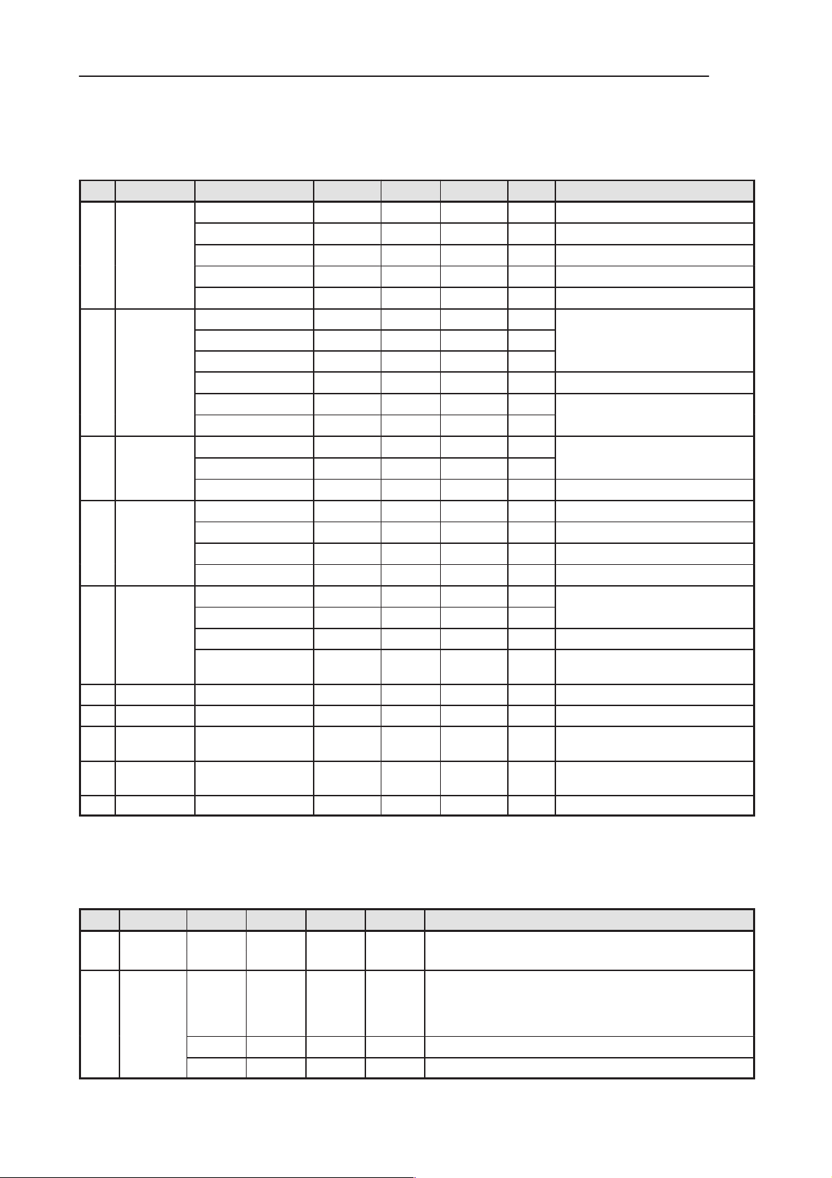
Table 3. Electrical characteristics of the system connector (X450) signals
Pin Name Parameter Min Typ Max Unit Notes
1 L_GND 0 0 0 V Supply ground
2 VIN Voltage in
Current in
Voltage in
Current in
Voltage in
Current in
3 CHRG_
4 SGND
5 XEAR
Output LOW 0 0.5 V Charger control (PWM) low
Output HIGH 2.4 2.85 V Charger control (PWM) high
PWM Frequency 32 Hz fast charger connected
PWM duty cycle 1 99 %
Output resistance 22 kΩ
Output AC imped-
ance
Series output capaci-
tance
Resistance to phone
ground
Output AC imped-
ance
Series output capacitance
Load AC impedance 16 300 Ω ref. to SGND (Headset)
Load AC impedance 4.7 10 kΩ ref. to SGND (Accessory)
Max. output level 1.8 Vpp no load
Load DC resistance 10 kΩ ref. to SGND (Accessory)
Load DC resistance 16 1500 Ω ref. to SGND (Headset)
DC voltage 2.8 V 44k pull–up to VBB
Earphone signal 0 70 630 mVrms HF–HFCM from COBBA_GJP HF
6.8
8.5 10.0
7.8 8.8
350
47 Ω ref. to GND
10 µF
330 Ω
47 Ω ref. to GND
10 µF
30
1.5
850
14.0 VmAUnloaded Standard Charger (ACP–7)
VACHAPS’ absolute max. input voltage
Fusing current
VmAUnloaded Fast Charger (ACP–9,
LCH–9)
Charging current
Charging current
output
issue 1 06/01
Page 3 – 13
Page 14
RAE-3
PAMS
3. RF+System Module BL8
Table 3. Electrical characteristics of the system connector (X450) signals (continued)
6 XMIC
7 MBUS Output LOW 0 0.22*VBB V Open drain output
8 DCE_TX
9 DCE_RX
10 DCE_DTR
11 GND 0 0 V Supply ground
12 RF_GND
13 RF_INTER-
NAL
14 RF_COM-
MON
15 RF_GND
Input AC impedance 2.2 kΩ
Max. input signal 1 Vpp
Output DC level 1.47 1.55 V Accessory muted (not for headset)
Output DC level 2.5 2.8 V Accessory unmuted
Bias current 100 600 µA
Output LOW current 2 mA
Pullup resistance 4.7 kΩ to VBB
Series resistance 270 Ω
Input LOW 0 0.3*VBB V
Input HIGH 0.7*VBB VBB V
Input LOW 0 0.3*VBB V To AccRxData
Input HIGH 0.7*VBB VBB V 220kΩ Pullup to VBB in bl8
Series resistance 270 Ω
Output LOW 0 0.22*VBB V From AccTxData
Output HIGH 0.8*VBB VBB V 47kΩ Pullup to VBB in bl8
Output current 4 mA
Series resistance 270 Ω
Input LOW 0 0.3*VBB V
Input HIGH 0.7*VBB VBB V
Series resistance 270 Ω
Technical Documentation
Data T erminal Ready input
Internal pullup max. 140mA
Accessory power output – refer to
VACC in NO TAG
To internal antenna – defined in RF
spec NO TAG
From RF – defined in RF spec
NO TAG
NotesUnitMaxTypMinParameterNamePin
Battery Connector
Table 4. Battery Connector (X100) Electrical Specifications
Pin Name Min Typ Max Unit Notes
1 VBATT 3.0 3.6 4.2 V Battery voltage
4.8 V Maximum voltage with charger
2 BSI
Page 3 – 14
0 2.8 V Battery size indication
System HW has 100kW 5% pull up resistor.
Battery removal detection (shorter contact)
(Threshold is 2.4V@VBB=2.8V)
221% kW Service battery pull down value
685% kW 4.2V Li–Ion battery pull down value
issue 1 06/01
Page 15
PAMS
RAE-3
Technical Documentation
3. RF+System Module BL8
Table 4. Battery Connector (X100) Electrical Specifications (continued)
NotesUnitMaxTypMinNamePin
3 BTEMP
4 BGND 0 0 V Battery ground – connected directly to system HW GND
0 1.4 V Battery temperature indication
Phone has 100k 5% pull–up resistor,
Battery package has NTC pull down resistor:
@+25C 47k 5%, B=40503%
0 1 kW Fast power up (in production)
Backup battery connector
Table 5. Backup battery connector X102
Pin Name Min Typ Max Unit Notes
1 VBACK IN 2.82 3.15 3.28 V Backup battery voltage from CHAPS
2 VBACK
OUT
1.8 3.3 V Backup battery voltage to CCONT/VBACK
@ Ibackup = 100mA
(not specified in CCONT spec)
VBACKIN and VBACKOUT are connected together in back up battery’s positive
terminal.
Table 6. Microphone contacts
Pin Name Min Typ Max Unit Notes
1 MICP 0.1 Vpp Pad P200
2 MICN 0.1 Vpp Pad P201
0.2 Vpp MICP–MICN differential voltage range
2.0 2.1 V MICP, MICN biasing output level
SIM card connector
Only Plug–in SIM (small SIM) cards are supported.
Table 7. SIM Connector (X101) Electrical Specifications
Pin Signal
Name
4 GND GND GND 0 0 V Ground
3 VSIM VCC (C1) Supply V oltage
6 SIM–DATA
SIM Con-
tact
Type
I/O (C7) Vout HIGH
I/O
Parameter Min Typ Max Unit Notes
Supply Voltage
Vout HIGH
Vout LOW
Trise/Tfall
Series Resistance
4.8
2.8
4.0
2.8
0
5.0
3.0
100
5.2
3.2
VSIM
VSIM
0.4
1
V
V
V
V
V
mS
W
5V SIM Card
3V SIM Card
5V SIM Card
3V SIM Card
3V/5V SIM Card
3V/5V SIM Card
(Vin not defined in CCONT
specification )
issue 1 06/01
Page 3 – 15
Page 16
RAE-3
PAMS
3. RF+System Module BL8
Table 7. SIM Connector (X101) Electrical Specifications (continued)
Signal
Pin
Name
Type
2 SIMRSTORST (C2) Vout HIGH
1 SIMCLK CLK (C3) Vout HIGH
5 VSIM VPP (C6) Supply Voltage
tact
Vout HIGH
Vout LOW
Trise/Tfall
Series Resistance
Vout HIGH
Vout LOW
Frequency
Trise/Tfall
O
Series Resistance
Supply Voltage
4.0
2.8
4.0
2.8
4.8
2.8
100
3.25
47
5.0
3.0
Technical Documentation
NotesUnitMaxTypMinParameterSIM Con-
VSIM
VSIM
0.4
100
VSIM
VSIM
0.4
25
5.2
3.2
V
V
V
ns
W
V
V
V
MHz
ns
W
V
V
5V SIM Card
3V SIM Card
3V/5V SIM Card
3V/5V SIM Card
5V SIM Card
3V SIM Card
3V/5V SIM Card
3V/5V SIM Card
3V/5V SIM Card
Programming voltage,
pin5 and pin3 tied together
MMC Connector
Table 8. MMC Connector Electrical Specifications
Pin Signal
Name
7 MMCDa
6 GND 6 / VSS2 0 0 V Ground
5 MMCClk
4 VMMC 4 / VDD powered on
3 GND 3 / VSS1 0 0 V Ground
2 MMCCmd
MMC Con-
tact
Type
7 / DAT[0] Output HIGH
I/O
5 / CLK Output HIGH
O
2 / CMD Output HIGH
I/O
Parameter Min Typ Max Unit Notes
Output LOW
Input HIGH
Input LOW
Series Resistance
Output LOW
Frequency
Series Resistance
powered off
Current
Output LOW
Input HIGH
Input LOW
Series Resistance
2.1
2.1
100
2.1
0
100
2.76 3.0 3.1
2.1
2.1
100
2.9
0.65
3.1
0.8
2.9
0.65
13
0
100
2.9
0.65
2.9
0.8
V
V
V
V
W
V
V
MHz
W
V
mA
V
V
V
V
W
There is 100kΩ Pullup to
VMMC in bl8
Supply voltage
Supply Current
Command/Response
There is 10kΩ Pullup to
VMMC in bl8
Data
Clock
Note: There is no pin 1 in connector
Page 3 – 16
(Not connected in MultiMediaCard mode; SPI mode not supported
issue 1 06/01
Page 17
PAMS
(P
IO)
RAE-3
Technical Documentation
3. RF+System Module BL8
Infrared interface
– IrDA and HP–SIR compatible
– Data rates from 9600bits/s to 115kbits/s
– Transmitter wavelength: min 880nm, max 900nm
UI Signals
Table 9. UI Connector
Pin Signal Name
Type
27,
VB Main
28,
29
15 FLVPP
not UI signal
16 VPROG
not UI signal
17 VBB 2.7 2.85 2.9 V Supply voltage
1,
GND 0 0 Supply ground
8,
21,
25,
30,
34,
41,
66,
70
49 COL0 MADLinda
62 COL1
60 COL2
35,59COL3
33,54COL4
55 COL5
56 COL6
61 COL7
53 COL8
From/To Parameter Minimum Nomi-
battery
Flash Vpp pins 15 and 16 con-
MADLinda
(Prog_IO)
Output high ”1” 0.8*VBB V
Output low ”0” 0.22*VBB V
Output current 2 mA
Input high ”1” 0.7*VBB V
Input low ”0” 0.3*VBB V
Series resistance 200
(Refer to COL0) Keyboard column
(Refer to COL0) Keyboard column
(Refer to COL0) Keyboard column
(Refer to COL0) Keyboard column
(Refer to COL0) Keyboard column
(Refer to COL0) Keyboard column
(Refer to COL0) Keyboard column
(Refer to COL0) Keyboard column
I/O
I/O
I/O
I/O
I/O
I/O
I/O
I/O
I/O
rog_
MADLinda
(Prog_IO)
MADLinda
(Prog_IO)
MADLinda
(Prog_IO)
MADLinda
(Prog_IO)
MADLinda
(Prog_IO)
MADLinda
(Prog_IO)
MADLinda
(Prog_IO)
MADLinda
(Prog_IO)
3.0 4.8 V Battery voltage
Maximum Unit Function
nal
nected in UL8
pins 15 and 16 connected in UL8
Keyboard column
W
issue 1 06/01
Page 3 – 17
Page 18
RAE-3
(P
IO)
63
(Prog_IO /
Command/Data select
(GPIO)
PAMS
3. RF+System Module BL8
Pin
Type
51 COL9
50 ROW0
69 ROW1
67 ROW2
65 ROW3
64 ROW4
ROW5LCDCD
32,
I/O
I/O
I/O
I/O
I/O
I/O
MADLinda
(Prog_IO)
MADLinda
rog_
MADLinda
(Prog_IO)
MADLinda
(Prog_IO)
MADLinda
(Prog_IO)
MADLinda
(Prog_IO)
MADLinda
Technical Documentation
Table 9. UI Connector (continued)
MinimumParameterFrom/ToSignal Name
(Refer to COL0) Keyboard column
Output high ”1” 0.8*VBB V Keyboard row
Output low ”0” 0.22*VBB V
Output current 2 mA
Input high ”1” 0.7*VBB V
Input low ”0” 0.3*VBB V
Series resistance 200
(Refer to ROW0) Keyboard row
(Refer to ROW0) Keyboard row
(Refer to ROW0) Keyboard row
(Refer to ROW0) Keyboard row
Output high ”1” 0.8*VBB V
nal
W
FunctionUnitMaximumNomi-
Serial LCD driver
57 ROW6
68 ROW7
58 ROW8
52 ROW9
42 BATT_REM
I/O
I/O
I/O
I/O
I/O
I
UIF)
MADLinda
(Prog_IO)
MADLinda
(Prog_IO)
MADLinda
(Prog_IO)
MADLinda
(Prog_IO)
MADLinda
Output low ”0” 0.22*VBB V
Output current 2 mA
Input high ”1” 0.7*VBB V Keyboard row
Input low ”0” 0.3*VBB V
Series resistance 200
(Refer to ROW0) Keyboard row
(Refer to ROW0) Keyboard row
(Refer to ROW0) Keyboard row
(Refer to ROW0) Keyboard row
Input high ”1” 0.7*VBB V Battery removal switch
Input low ”0” 0.3*VBB V
Series resistance 200
W
W
Page 3 – 18
issue 1 06/01
Page 19
PAMS
(
)
O
(),
()
(UIF)
(Ph
LCD)
(UIF)
(Ph
LCD)
(PWM)
l
(PWM)
backligh
l
(GPIO)
l
(GPIO)
RAE-3
Technical Documentation
Pin
Type
11
GenSClk
9
GenSDIO MADLinda
MADLinda
UIF),
(and to
CCONT)
O
3. RF+System Module BL8
Table 9. UI Connector (continued)
MinimumParameterFrom/ToSignal Name
Output high ”1” 0.8*VBB V
Output low ”0” 0.22*VBB V
Output current 2 mA
Frequency 0 3.25 MHz 3.25MHz during
Series resistance 200
Output high ”1” 0.8*VBB V
Output low ”0” 0.22*VBB V
Output current 2 mA
Series resistance 200
nal
W
W
FunctionUnitMaximumNomi-
Serial LCD driver
clock (Phone LCD
Phone LCD access,
2.17MHz during
CCONT access
Serial LCD driver data
one
12
LCDEN MADLinda
10
LCDPWM MADLinda
31
BACKPWM MADLinda
6
LCD_PWR MADLinda
Output high ”1” 0.8*VBB V
O
O
O
O
Output low ”0” 0.22*VBB V
Output current 2 mA
Series resistance 200
Output high ”1” 0.8*VBB V
Output low ”0” 0.22*VBB V
Output current 2 mA
Series resistance 200
Frequency 0 50.7
Output high ”1” 0.8*VBB V
Output low ”0” 0.22*VBB V
Output current 2 mA
Series resistance 200
Frequency 0 231
Output high ”1” 0.8*VBB V
Output low ”0” 0.22*VBB V
Output current 2 mA
Series resistance 200
Serial LCD driver chip
select
W
PWM for PDA LCD
contrast contro
W
kHz
PWM for PDA LCD
W
Hz
PDA LCD power contro
W
one
t contro
14
issue 1 06/01
LCDRSTX MADLinda
O
Output high ”1” 0.8*VBB V Phone LCD reset
Output low ”0” 0.22*VBB V
Output current 2 mA
Series resistance 200
W
Page 3 – 19
Page 20

RAE-3
(GPIO)
b
l
(LCD)
(LCD)
(LCD)
l
PAMS
3. RF+System Module BL8
Pin
Type
13
KBLIGHTS MADLinda
O
5
LCDDa0 MADLinda
O
26 LCDDa1
24 LCDDa2
38 LCDDa3
20 LCDDa4
36 LCDDa5
37 LCDDa6
22 LCDDa7
19 LCDDa8
23 LCDDa9
39 LCDDa10
7 LCDDa11
MADLinda
(LCD)
O
MADLinda
(LCD)
O
MADLinda
(LCD)
O
MADLinda
(LCD/GPIO)
O
MADLinda
(LCD/GPIO)
O
MADLinda
(LCD/GPIO)
O
MADLinda
(LCD/GPIO)
O
MADLinda
(LCD/GPIO)
O
MADLinda
(LCD/GPIO)
O
MADLinda
(LCD)
O
MADLinda
(LCD)
O
Technical Documentation
Table 9. UI Connector (continued)
MinimumParameterFrom/ToSignal Name
Output high ”1” 0.8*VBB V
Output low ”0” 0.22*VBB V
Output current 2 mA
Series resistance 200
Output high ”1” 0.8*VBB V PDA LCD data
Output low ”0” 0.22*VBB V
Output current 2 mA
Series resistance 200
(refer to LCDDa0) V PDA LCD data
(refer to LCDDa0) V PDA LCD data
(refer to LCDDa0) V PDA LCD data
(refer to LCDDa0) V PDA LCD data
(refer to LCDDa0) V PDA LCD data
(refer to LCDDa0) V PDA LCD data
(refer to LCDDa0) V PDA LCD data
(refer to LCDDa0) V PDA LCD data
(refer to LCDDa0) V PDA LCD data
(refer to LCDDa0) V PDA LCD data
(refer to LCDDa0) V PDA LCD data
nal
W
W
FunctionUnitMaximumNomi-
Phone LCD & key-
oard light contro
2
DISPClk MADLinda
40
LLClk MADLinda
Page 3 – 20
Output high ”1” 0.8*VBB V PDA LCD data clock
O
O
Output low ”0” 0.22*VBB V
Output current 2 mA
Frequency 8.67 MHz
Series resistance 200
Output high ”1” 0.8*VBB V
Output low ”0” 0.22*VBB V
Output current 2 mA
Frequency 10.8 kHz
W
PDA LCD line data
atch to display
issue 1 06/01
Page 21

PAMS
(LCD)
(GPIO)
(
O
(LCD)
signal
RAE-3
Technical Documentation
Pin
Type
4
FSP MADLinda
O
3
DISPON MADLinda
O
18
LCDM
MADLinda
3. RF+System Module BL8
Table 9. UI Connector (continued)
MinimumParameterFrom/ToSignal Name
Series resistance 200
Output high ”1” 0.8*VBB V
Output low ”0” 0.22*VBB V
Output current 2 mA
Frequency 51.6 Hz
Series resistance 200
Output high ”1” 0.8*VBB V
Output low ”0” 0.22*VBB V
Output current 2 mA
Series resistance 200
Output high ”1” 0.8*VBB V
Output low ”0” 0.22*VBB V
Output current 2 mA
Frequency 10.8 kHz
Series resistance 200
nal
W
W
W
W
FunctionUnitMaximumNomi-
PDA LCD frame start
sync pulse
PDA LCD display logic
on/off control,
(MPUGenOut7 internally in MADLinda)
PDA LCD modulation
(Polarity change)
48 EARP
47 EARN
43,44SPKP
45,46SPKN
COBBA_GJP Maximum Output swing
O
COBBA_GJP Maximum Output swing
O
Audio Amp Output level 1.8 Vrms HF Speaker
O
Audio Amp Output level 1.8 Vrms (signal details
O
Vpp
Vpp
EARP/N Offset –50 50 mV
Load resistance 32
Load resistance 8
System – RF interface
Table 10. AC and DC Characteristics of signals between RF and System blocks
Signal name From To Parameter Mini-
VBATT Main
battery
VREF CCONT
(VREF)
VXO CCONT
(VR1)
VSYN_1 CCONT
(VR4)
PA Voltage 3.0 3.6 4.8 V PA supply voltage
RF
(HAGAR)
VCTCXO Voltage 2.7 2.8 2.85 V
Vdd_bb,
LNAs
Voltage 1.478 1.5 1.523 V Reference voltage
Voltage 2.7 2.8 2.85 V Supply voltage for LNAs
mum
2.36 2.5 V Earpiece
2.36 2.5 V (signal details
Typi-
cal
Maximum
Unit Function
NO TAG)
W
NO TAG)
W
(NO TAG)
for RF (NO TAG)
Supply voltage for
VCTCXO (NO TAG)
and Vdd_bb (NO T AG)
issue 1 06/01
Page 3 – 21
Page 22

RAE-3
()
PAMS
3. RF+System Module BL8
Technical Documentation
Table 10. AC and DC Characteristics of signals between RF and System blocks (continued)
FunctionUnitMaxi-
ers, LO buffers, prescalers and VCO (NO TAG)
charge pump regulator
(NO TAG)
+ mixer + DTOS
(NO TAG)
modulator (NO T AG)
HAGAR reset, active
LOW
HAGAR synthesizer interface enable
HAGAR synthesizer interface control data
HAGAR synthesizer interface clock
Automatic frequency
control signal for
VC(TC)XO
High stability clock signal from RF block,
Series capacitance
VSYN_2 CCONT
VCP CCONT
VRX CCONT
VTX CCONT
HAGARRSTX
SENA1 MADLinda HAGAR
SDATA MADLinda HAGAR
SCLK MADLinda HAGAR
AFC COBBA_GJP VCTCXO
RFC VCTCXO MADLinda
(VR3)
(5V5)
(VR2)
(VR5,VR7)
MADLinda HAGAR
HAGAR,
VCO
Charge pump
regulator
HAGAR Voltage 2.7 2.8 2.85 V Supply voltage for LNA2
HAGAR Voltage 2.7 2.8 2.85 V Supply voltage for TX
ParameterToFromSignal name
Voltage 2.7 2.8 2.85 V Supply voltage for divid-
Voltage 4.8 5.0 5.2 V Supply voltage for PLL
Output high
”1”
Output low
”0”
Output Current
Output high
”1”
Output low
”0”
Output Current
high ”1” 0.8*VBB VBB V
low ”0” 0 0.22*VBB V
Output Cur-
rent
Data rate 3.25 Mbit/s
Output high
”1”
Output low
”0”
Output cur-
rent
Clock rate 3.25 MHz
Voltage 0.046 2.254 V
Resolution 11 bits
Load resis-
tance (dynamic)
Load resistance (static)
Frequency 13 MHz
Signal ampli-
tude
Load resis-
tance
Load capaci-
tance
Minimum
0.8*VBB VBB V
0.8*VBB VBB V
0.8*VBB VBB V
10 kW
0.5 1.0 2.0 Vpp
10 kW
Typi-
cal
0 0.22*VBB V
0 0.22*VBB V
0 0.22*VBB V
1 MW
mum
2 mA
2 mA
2 mA
2 mA
1 nF
Page 3 – 22
issue 1 06/01
Page 23

PAMS
RX si
d
RX si
d
the TX I/Q
I/Q
RAE-3
Technical Documentation
3. RF+System Module BL8
Table 10. AC and DC Characteristics of signals between RF and System blocks (continued)
FunctionUnitMaxi-
Single ended in–phase
gnal to baseban
Single ended quadrature
gnal to baseban
Reference voltage
for RX signals
Differential in–phase
TX baseband signal for
Differential quadrature
phase TX baseband sig-
nal for the TX
lator
Transmitter power control enable
RXIP HAGAR COBBA_GJP
RXQP HAGAR COBBA_GJP
RXREF COBBA_GJP HAGAR
TXIP/
TXIN
TXQP/TXQN COBBA_GJP HAGAR
TXP MADLinda HAGAR
COBBA_GJP HAGAR
ParameterToFromSignal name
Output level 300 1400 mVpp
Input imped-
ance
Input capaci-
tance
Output level 300 1400 Vpp
Input imped-
ance
Input capaci-
tance
Output Volt-
age
Output Im-
pedance
External seri-
al load
Load Current 100 mA – sink or source
Differential
voltage swing
DC level 1.165 1.2 1.235 V
Output im-
pedance
Differential
voltage swing
DC level 1.165 1.2 1.235 V
Differential
offset voltage
(corrected)
Diff. offset
voltage temp.
dependence
Output impedance
Output high
”1”
Output low
”0”
Output Current
Minimum
1.15 1.2 1.25 Vpp
1.022 1.1 1.18 Vpp
1.022 1.1 1.18 Vpp
2.1 2.9 V
Typi-
cal
1 MW
8 pF
1 MW
8 pF
3 200 W
9 kW
0 0.8 V
mum
500 W
+/– 2.0 mV
+/– 1.0 mV
500 W
2 mA
modulator
modu-
issue 1 06/01
Page 3 – 23
Page 24

RAE-3
PAMS
3. RF+System Module BL8
Technical Documentation
Table 10. AC and DC Characteristics of signals between RF and System blocks (continued)
FunctionUnitMaxi-
Transmitter power control voltage
TXC
COBBA_GJP HAGAR
ParameterToFromSignal name
Voltage Min
level
Voltage Max
level
Output impedance
active state
Output impedance
power down
state
External resistance
External capacitance
Settling time 10 ms
Minimum
0.12 0.18 V
2.27 2.33 V
high Z
10 kW
Typi-
cal
mum
200 W
10 pF
Page 3 – 24
issue 1 06/01
Page 25

PAMS
RAE-3
Technical Documentation
Functional Description
Modes of Operation
There are three main operation modes in the system when power is on:
– Running
– Idle
– Deep Sleep
Note that phone can be either on or off in each of power on states.
3. RF+System Module BL8
Power OFF
Idle Running Deep Sleep
(VCXO ON) (VCXO ON) (VCXO OFF)
Figure 3. Basic Operation Modes of RAE-3 (simplified scheme)
Power saving modes are entered under SW control. Returning to running mode
is activated by interrupt (generated internally by MADLinda or from CCONT).
Clocking Scheme
The 26MHz main clock frequency is generated by the VCTCXO located in the
RF section. This clock is divide in HAGAR to 13MHz. Clock signal is buffered
to low level sine wave clock signal (RFC) and fed to system HW side. There it
is connected to MADLinda clock input. The MPU within MADLinda can stop the
clock by shutting off the VCTCXO’s supply voltage (VXO) via CCONT.
Battery voltage
high enough
Reset
Power Up
Interrupt
No tasks to run
Too low
Battery
voltage
or
Battery
removed
Interrupt
Deep Sleep conditions met
The CCONT provides a 32kHz sleep clock generated from 32.768kHz quartz
crystal. This clock signal is used internally in CCONT to run the RTC and
routed to MADLinda (SLEEPCLK). Sleep clock is used to run MADLinda when
the main clock is shut down. A backup battery keeps the RTC running if the
main battery is disconnected.
issue 1 06/01
Page 3 – 25
Page 26

RAE-3
PAMS
3. RF+System Module BL8
Other clock signals are generated inside MADLinda using PLLs and clock dividers which are controlled by SW. The maximum clock frequency in the MPU side
is 52MHz and in the DSP side 78MHz.
NO TAG shows the System HW clocking scheme.
Power Control and Reset
In normal operation the system HW is powered from the main battery. An external charger can recharge the battery while also supplying power to RAE-3. The
supplied charger is so called performance charger (ACP–9), which can deliver
850mA.
The power management circuitry provides protection against over–voltages,
charger failures and pirate chargers etc. that would otherwise cause damage to
RAE-3.
Following chapters give an overview about power management issues.
Technical Documentation
Power Distribution
Figure 4 shows the power distribution of RAE-3.
Power supply components – CCONT, VBB, Vcore, VACC and VMMC regula-
tors – and the audio amplifier are powered with main battery voltage. Main battery voltage is also fed to RF part for RF power amplifier (PA) and to the UI
module for backlight and LCD supply.
Separate linear regulator generates the 2.8V VBB power supply. VBB powers
most of the system HW portions including MADLinda, memories, COBBA_GJP’s digital supply and the logic parts of the IR transceiver. It also supplies 2.8V to the UI module.
Separate DC/DC regulator generates the 1.8V Vcore voltage. Vcore is used as
supply for the MADLinda core and as IO voltage for XIP memories.
CCONT’s V2V output is used as enable for VBB and Vcore regulators.
VSIM regulator of CCONT is used to generate either 3V or 5V supplies for SIM
card. This is required so that RAE-3 can support both 3V and 5V SIM cards.
VR6 generates the voltage for COBBA_GJP’s analogue part.
CCONT generates the reference voltage VREF for COBBA_GJP and HAGAR.
It also generates the 5V supply voltage (V5V) for RF. In RF side there is separate regulator that drops this voltage to 4.7V for DCT4 RF use.
Regulators VR1 to VR5 inside CCONT generate voltages for RF HW. Regulator
control signals come from MADLinda.
Separate 3V linear regulator is used to power the MMC card.
Another 3V linear regulator is used to generate accessory power that can be
fed through system connector for external accessory.
Page 3 – 26
issue 1 06/01
Page 27

issue 1 06/01
3.7V
BATTERY
VBATT
VB
PAMS
Technical Documentation
VPC
(HAGAR)
Figure 4. Power Distribution of RAE-3
VBB
CCONT
2.8V
LINEAR
REG.
VB
VBATT
PA
VB_CCONT
V2V
1.8V
DC/DC
MMC
Audio
Amp.
VR
1
VXO VSYN_2
VCTCXO
+ buffers
VR
2
VR
3
VRX
3.0V
LINEAR
REG.
VR
4
VSYN_1
LNA
Backlight
Power
VR
5
VTX
VR6VR
VCOBBA
COBBA
Analog
IR
LEDs
7
3.0V
LINEAR
REG.
VSIM VREF V5V
VSIM
COBBA
HAGAR
bias
SIM
Vacc
Power
Out
VXOPWR
SYNTHPWR
TXPA
VCP
3. RF+System Module BL8
Page 3 – 27
MADLinda VBB
FLASH
SERIAL FLASH
SDRAM
IR LOGIC
COBBA DIGIT.
INTERFACES
CMT LCD
PDA LCD
VBB
MADLinda Core
LMM
MADLinda I/O
FLASH I/O
Vcore
TXC
TXP
HAGAR RF–IC
RX / TX parts
PLL
RXREF
HAGARRSTX
VCHP
VCO
4.7V
LINEAR
REG.
HAGARRSTX
RAE-3
SYSTEM HW P ARTS
Page 28

RAE-3
PAMS
3. RF+System Module BL8
Power up
When main battery is connected to device, powering on circuitry keeps CCONT
PWRONX/WDDISX pin connected to ground through10kW resistor as long as
CCONT releases the PURX reset signal. This activates the CCONT immediately when battery is connected.
When the CCONT is activated, it switches on internal baseband and core regulators and generates a power up reset signal PURX for MADLinda. External
Vcore and VBB regulators are powered up, Vcore slightly before VBB.
After 62ms CCONT releases the PURX reset signal. When the PURX is released, MADLinda releases the system reset (ExtSysResetX), the Flash reset
(FLRPX) and internal reset signals and starts the boot program execution. Note
that from battery plug in to PURX release it takes about 100ms since there is
no power in CCONT.
The GenSDIO pin is connected low with pull–down resistor so that booting
starts from MADLinda’s internal boot ROM. If booting is successful (and the
programming device is not connected) the program execution continues from
external program memory.
Technical Documentation
The CMT power switch (on the cover) is read as a normal keyboard input. It is
not connected to CCONT. CMT Power switch only turns the phone functionality
on or off (SW implementation).
Power Off
RAE-3 electronics is powered off only if the main battery voltage drops below
the power off SW limit. This happens when the main battery discharges or is
removed. When battery voltage drops below SW limit, CCONT is powered
down by letting CCONT’s watch dog to go off.
Early warning of battery removal is generated by the battery removal switch.
Switch connects MADLinda’s MPUGenIO6 to ground when user presses the
locking latch of the battery.
Only phone functionality is ”powered off” when the CMT power switch is
pressed. If the main battery is removed when the CMT is on, the SIMIF in
MADLinda powers down the SIM.
Charging
Charging of main battery can be started in any operating mode. The battery
type and capacity are identified by MADLinda by measuring a pull–down resistor connected to BSI contact inside the battery pack. Charging software running
in MADLinda’s MPU measures the battery voltage, size, current and temperature.
In Standard charger concept (2–wire charger) the power management circuitry
controls the charging current delivered from the charger to the main battery.
The charging–current switch inside CHAPS is controlled with 1Hz PWM signal,
Page 3 – 28
issue 1 06/01
Page 29

PAMS
RAE-3
Technical Documentation
generated by CCONT. Note that Standard charger is not sold with RAE-3, but it
is accepted.
In performance charging concept (3–wire charger) a 32Hz PWM signal is fed to
the charger (CHRG_CTRL in system connector). This high rate keeps the
charging–current switch in CHAPS continuously connected.
The PWM pulse width is controlled by the MPU in MADLinda which sends a
control value to CCONT through a serial control data bus. The main battery
voltage rise is limited to a specified level by turning the switch off. Lower limit
(4.8V) in CHAPS is permanently selected because only lithium batteries are
supported. Charging current is monitored by measuring the voltage drop across
a sensor resistor.
I
charge in
CHARGE
CONTROL
(PWM in 3–wire
concept)
CHAPS IC
(CONTROL
SWITCH)
* Wake–Up Charge
* Voltage protect
CHARGE
CONTROL
(PWM in 2–wire
concept)
3. RF+System Module BL8
BATTERY
PACK
* 4.2V Li–Ion
BATTERY SENSING:
* Voltage
* Size/type
* Temperature
I
supply out
CHARGER
SENSING
Figure 5. Block diagram of charge control in RAE-3
Resets and Watchdogs
Power–up reset signal, PURX, is the main reset in RAE-3. PURX is generated
by CCONT during power–on. The watchdog within CCONT is enabled and
must be fed periodically to keep CCONT (and whole device) powered on.
PURX –signal is connected to MADLinda’s reset input (PURX). Figure 6 shows
the board/module level reset scheme in RAE-3.
CCONT IC
* A/D conversion
* PWM output
* Serial data in/out
CHARGER
AND BATTERY
INTERRUPT
SERIAL DATA
ASIC
MPU
DSP
*
Connect/disconnect
detection
MADLinda IC
issue 1 06/01
Page 3 – 29
Page 30

RAE-3
PAMS
3. RF+System Module BL8
CCONT
CCONT
WATCHDOG
UI conn.
(To CMT LCD
Controller)
SimCardRstX
PURX
LCDRSTX
MADLinda
Technical Documentation
HAGAR
(RF)
HAGARRSTX
COBBARSTX
COBBA
ExtSysResetX
SER FLASH
FLRPX
FLASH
Figure 6. Board/Module level reset scheme
PURX resets the whole MADLinda. ExtSysResetX signal follows PURX activity
during reset. After reset this signal can be configured as IO and thus controlled
by SW with MPUGenOut8 control bit. The ExtSysResetX is connected to serial
Flash reset pin.
The LCD driver reset signal (LCDRSTX) is a MADLinda general purpose output
controlled by MPU SW.
Flash memory interface in Traffic Controller’s MEMIF block includes Flash reset/power down signal (FLRPX). FLRPX signal follows PURX activity during reset. After reset this signal can be controlled by MPU SW. Signal is connected to
XIP Flashes.
MADLinda’s SIM interface block generates the reset signal (SimCardRstX) for
the SIM. This signal is fed through CCONT, which makes any level shifting necessary according to the voltage level of the SIM card in use.
COBBA_GJP reset signal (COBBARSTX) is DSPGenOut0 general purpose
output controlled by DSP SW. Reset state of the pin is LOW.
HAGAR reset signal (HAGARRSTX) is DSPGenOut1 general purpose output
controlled by DSP SW. Reset state of the pin is LOW.
Page 3 – 30
issue 1 06/01
Page 31

PAMS
RAE-3
Technical Documentation
System to interface
In following chapters the blocks of system HW in SYSTEM part of BL8 schematics and functions related to each interface are described.
The blocks include: CPU, MEMORIES, MMC, IRDA, UI, SYSCON, AUDIO_RFI
and POWER.
Component placement diagrams are in the A3 section.
CPU block
Main components in the CPU block comprise:
– MADLinda ASIC (D300), package 240 m*BGA
– Hall switch TLE4916 (V301)
MADLinda is the main ASIC for RAE-3’s single processor system. MADLinda is
used as engine processor for both CMT and PDA functions. The pins are ot
listed because it is not possible to access them except at measurement points.
3. RF+System Module BL8
Hall sensor switch is used to detect lid position (open/close). Magnet for detection is in lid part of RAE-3. Hall device’s open drain output is pulled up with external 100k
magnetic field (lid open).
W resistor (R302). Output goes to low state when the sensor is not in
MEMORIES block
Main components in the block include:
– three 2Mx16 (32Mbit) Flash memories (D351, D352, D353)
– SDRAM 4Mx16 (64Mbit) (D350)
– Serial Flash 32Mbit (D354)
XIP Memories
The MPU program code resides in three Flash memories. 128kBytes PPM area
for language depend program parts is locate to one of the XIP flashes. Also
4*8kBytes PMM area and 4*8kBytes for EEPROM emulation (EEEMU) is located to that same flash device.
Flashes are 4Mbyte (2Mx16) 80ns asynchronous ’Advanced Boot Block’ devices packed in 48 pin CSP (VFBGA48).
XIP memories are supplied from 2.8V VBB and I/O voltage from 1.8V Vcore.
issue 1 06/01
Page 3 – 31
Page 32

RAE-3
PAMS
3. RF+System Module BL8
X400
UI
Connector
D351
V
PP
D352
VPP
D353
VPP
Technical Documentation
Connection in UL8 Flex
15 16
D300
MADLinda
DSPGenOut2
SDRAM Memory
Synchronous DRAM is used as working memory and PDA display buffer
memory. MADLinda includes a separate 16 bit wide interface for SDRAM device. Interface supports also byte accesses. Supported memory clocking
speeds are 13MHz and 52MHz.
The SDRAM is 64Mbits (8Mbyte) 104MHz device in 52–pin CSP. Organisation
of the memory is 4Mx16 with byte accesses possibility. Nominal supply voltage
Vcc is 2.8V and it is supplied from the common VBB voltage.
SDRAM supports self refresh mode. This mode is used in Deep Sleep mode
when all clocks are off to preserve SDRAM data . All memory contents are lost
when memory is un–powered, so when battery is removed or battery voltage
drops under power off voltage.
Serial Flash Memory
XIP Flashes
Figure 7. XIP Flash Vpp connection
Half of the Serial Flash memory is used as Flash file system memory (user
data). The other half is used to load parts of application code to serial Flash
(For running these applications are first copied to SDRAM). Serial interface to
memory is controlled by the Serial Flash interface block in MADLinda.
Used memory is 32Mbits (4Mbytes) SPI type Flash in 44 pin CSP package
(CBGA44). Page size is 528 bytes. Memory is powered from 2.8V VBB. Maximum used clock rate is 13MHz.
Page 3 – 32
issue 1 06/01
Page 33

PAMS
RAE-3
Technical Documentation
MMC block
Main components in MMC block are:
– MMC connector (X001)
– ESD protection zener array (V001)
MultiMediaCard mode type serial interface to MultiMediaCard is controlled by
the MMC interface block in MADLinda. The MMC interface includes two serial
lines, command and data, and one clock line that is used to clock serial transfers in both lines. Used clock frequency is 13MHz.
SPI mode MultiMediaCards are not supported in RAE-3.
MultiMediaCard is powered with 3.0V supply using controllable regulator.
Mechanical switch is used to indicate when the lid covering the MultiMediaCard
(and SIM) is opened. Switch is integrated to RAE-3 B–cover mechanics. In BL8
there is only contact pad J001 for the signal.
Hot swap as specified in MultiMediaCard System Specification is not supported. MultiMedaCard must be powered off (VMMC turned off) when lid is
opened.
3. RF+System Module BL8
IRDA block
Main component in IRDA block is the IR transceiver TFDU5102 (N050).
Data transmitting and receiving through IR interface is handled by IrDA block
inside MADLinda. MPU controls the interface.
UI block
Components in UI block include:
– Board–to–board UI connector (X400)
– Integrated EMI/ESD filtering components (Z400, Z401, Z402, Z403, Z404)
QWERTY –flex module UL8 is connected to UI connector. DL2 UI module is
connected to system HW through UL8.
Phone LCD Interface
Phone LCD interface is controlled by MPU using LCDSIO part of MADLinda’s
internal UIF block. This same serial control interface is used also to command
the CCONT. Phone LCD resetting and backlight control of LCD and phone keys
are controlled by MPU using signals from MADLinda’s GPIO.
Keyboard Interface
Keyboard interface is controlled by MPU using programmable I/O block inside
MADLinda. I/O signal matrix is used to read both PDA keyboard (qwerty and
soft keys) and phone keypad.
To detect the key press ROWs are programmed to give interrupt when any of
the keys is pressed. After key press detection SW polling is used to find out
pressed key.
issue 1 06/01
Page 3 – 33
Page 34

RAE-3
PAMS
3. RF+System Module BL8
Earpiece and HF Speaker lines
Earpiece and speaker lines come from the AUDIO_RFI block.
Battery removal signal
BATT_REM signal comes from the battery removal switch.
SYSCON block
Main components in system connector block include:
– System connector (X450) (pads for system connector’s spring contacts)
– Coaxial connector for antenna cable (X499)
– ESD protection zener array (V451)
For protecting the communicator against ESD spikes and EMI at the system
connector, all lines are equipped with TVS and filtering devices located next to
the system connector.
Technical Documentation
The system connector includes the following group of contacts:
– DC jack for external plug–in charger and contacts for desktop charger
– Contacts for external audios
– Contacts for serial connections
– External RF connector with switch
Externally, the system connector resembles the system connector in N9110
Communicator. Figure 8 shows the pads on PWB and Figure 9 shows the connector. Serial connection signals are named in RAE-3’s connector according to
DCE type equipment (as in RAE–2). This means that DCE_RX and DCE_DCD
(MBUS line) are outputs and DCE_TX and DCE_DTR are inputs.
1413
101189
123
15 12
6745
Page 3 – 34
Figure 8. Pads for system connector on top side of BL8
issue 1 06/01
Page 35

PAMS
RAE-3
Technical Documentation
L_GND
DC_jack
VIN
CHRG_CTRL
DCE_TX
SGND
XEAR
Guiding and locking holes
DCE_RX
XMIC
DTR
GND Spring contacts
MBUS
External RF with switch
3. RF+System Module BL8
to PWB
Serial connections
Serial interface signals are MBUS (DCE_DCD) [MBUS], DCE_RX [AccTxData],
DCE_TX [AccRxData] and DCE_DTR [DTR]. First name is the contact name in
the system connector and in square brackets is given the signal name used in
schematics. Note that all these signals are logic level signals thus interface
buffering/level sifting according some serial interface standards is done outside
RAE–3.
MBUS is normally connected to PUP USART. When PUP USART is selected to
be connected to transmit and receive lines (FBUS use) MBUS is not usable as
a serial signal. In synchronous mode MBUS is used as USART’s clock input.
Synchronous mode is used in DCT3 type Flashing.
DTR handshaking input is connected to MPUGenIO0. Accessory power output
(VACC) is also fed through the DCE_DTR pin. Diode V489 prevents cable’s signal output to supply power to BL8, when main battery is not connected, and accessory power regulator to supply 3V directly to MADLinda’s input. Pullup R310
is thus needed to generate the high level state of DCE_DTR input to MPUGenIO0.
Figure 9. System Connector
External Audio Interface
External audio signals, XMIC and XEAR, come from AUDIO_RFI block (see
p.38 ). An external headset accessory, car kit or loop set can be connected to
the external audio lines. External audio lines are also used to detect different
accessories.
issue 1 06/01
Page 3 – 35
Page 36

RAE-3
PAMS
3. RF+System Module BL8
Charger Interface
Charger voltage input line V_IN is connected through 1.5A fuse (F450) to
CHAPS (charger control) ASIC’s VCH inputs. Divided (47k/4k7) V_IN voltage
level is connected to CCONT’s VCHAR ADC input.
Charger controlling PWM output line, CHRG_CTRL, comes from CCONT’s
PWM output (PWM_OUT).
External RF
External RF signal comes from RF section of BL8. RF connector in system connector includes switch for external/internal signal routing. When external RF
plug is not connected to the system connector, RF signal is connected to coaxial antenna cable connector (X499).
POWER block
Power block includes following functions:
– supply voltage generation for system and RF parts and 2.8V to UI
– control of main battery charging
– power on and power off controlling and reset generation
– RTC and RTC backup control
– sleep clock generation
– SIM interface
– A/D conversions
– powering of MultiMediaCard
– Accessory power output generation (through System Connector)
Technical Documentation
Main components in power block are:
– CCONT2M power ASIC (N100)
– CHAPS charging control ASIC (N101)
– Linear regulator (N102) for VBB
– DC/DC switching regulator (V105) for Vcore
– Linear regulator (N103) for MultiMediaCard powering (VMMC)
– Linear regulator (N104) for Accessory power output (VACC)
– FET (V108) for control of regulators N102 and V105
– 32.768kHz crystal oscillator (32k XTAL B100)
– 2.7V reset device (D101), NC7SZ175 D–flip–flop (D102) and fets (V102,
V106) for power on & off control
– 2.0V reset device (D100) for backup disconnection
– ESD protection zener array (V103) for SIM interface
– 2–pin connector (X102) for backup battery (contacts for positive terminals)
– Battery connector (X100) for main battery
– SIM card connector (X101)
Clocking, powering, charging and reset issues of CCONT and CHAPS are covered in separate chapters .
Backup battery is connected to CCONT’s VBACK input and it is charged from
CHAPS’ VBACK supply. Backup battery’s positive contacts are made so that
Page 3 – 36
issue 1 06/01
Page 37

PAMS
RAE-3
Technical Documentation
VBACK from CHAPS is connected to CCONT only when the battery is installed
to the connector X102. Backup battery is located on top of RF shield A501 and
grounded through the shield.
2.0V reset device (D100) disconnects backup battery if it’s voltage drops too
much. This prevents deep discharging which would permanently harm the
backup battery.
3.0V VMMC supply voltage for MultiMediaCard is generated with linear regulator (N103) from filtered battery voltage (VB). Regulator is controlled with the
MMC_PWR signal from MADLinda MPUGenIO5.
Accessory power output (VACC) through the system connector’s DCE_DTR
line is generated with 3.0 volts linear regulator (N104) from filtered battery voltage (VB). Regulator’s feed back resistor are internally disconnected from the
output pin when the regulator is not enabled, so output will not affect DCE_DTR
line’s normal signal usage. VACC regulator is controlled with VACC_CTRL –signal from MADLinda’s MPUGenOut1. .
3. RF+System Module BL8
Use of CCONT ADC channels
Following table describes the analogue signals measured with CCONT’s A/D
converter.
Table 11. ADC in CCONT
PIN
CCONT PIN
no.
A1 RSSI Not used 0.1V .. Vref
B1 ICHAR – Charger current measured through a 0.22W resistor X101 0.1V .. VBAT+0.4V
D2 VBAT VB_CCONT Main battery voltage 0.1V .. VBAT
A3 VCHAR V_IN Charger voltage (through voltage division) 0.1V .. V ref
D5 VCXOTEMP Not used 0.1V .. Vref
B3 BSI BSI Main battery size indicator 0.1V .. Vref
C4 BTEMP BTEMP Main battery temperature 0.1V .. Vref
A2 EAD HEADDET External accessory detect – HEADDET 0.1V .. Vref
NAME
The type of the connected main battery is identified from the BSI line’s voltage
level. This voltage is formed by the system HW’s pull–up resistor (100kW) and
battery back’s pull–down resistor. Level is read with CCONT’s BSI A/D input.
CON-
NECTED
SIGNAL
MEASURES ADC input range
The BSI contact on the battery connector is also used to detect when the battery is being removed to be able to shut down the operations of the SIM card
before the power is lost. The BSI contact is shorter than the supply power contacts so this contact breaks first when the battery pack is removed, giving some
time for the shut–down operations.
The temperature of the main battery is read from the BTEMP line’s voltage level. This voltage is formed by the system HW’s pull–up resistor (100kW) and battery pack’s NTC resistor. Level is read with CCONT’s BTEMP A/D input.
issue 1 06/01
Page 3 – 37
Page 38

RAE-3
PAMS
3. RF+System Module BL8
AUDIO_RFI block
The function of the AUDIO_RFI block is to interface between the digital world of
the System Hardware and the analogue world of the audio and RF stages.
Main components are:
– COBBA_GJP (N200)
– Hands free audio amplifier (N201)
– FET (V200) for amplifier shut down control
– V202 for mic lines’ EMI filtering/ESD protection
COBBA_GJP is a combined AUDIO– and RF–codec for DCT3 generation
phones with serial RF TxIQ & RxIQ data lines and serial control interface.
RFI
COBBA_GJP handles the following RFI functions:
– IF receiving with I/Q separation and A/D conversion (RxI, RxQ)
– I– and Q–transmit and D/A conversion (TxI, TxQ)
– transmit power control (TXC) D/A conversion
– Automatic frequency control (AFC) D/A conversion
Technical Documentation
Audio
Digital communication between COBBA_GJP and MADLinda is handled by
MADLinda’s SerialMFI block which controls both serial RF TxIQ and RxIQ data
transfer and COBBA’s control interface.
RAE–3 includes both normal phone audio and personal handsfree (PHF) audio
functionality. Handsfree mode is implemented by speaker and normal mode by
earpiece. Speaker and earpiece are not located on the BL8 module. Signals for
speaker and earpiece are passed through the UI connector. Only one high sensitivity microphone will be used for both modes. On the BL8 module there are
contacts pads (P200, P201) where microphone is connected with spring contacts.
Analogue to digital conversion (ADC) of RAE-3’s microphone signals and digital
to analogue conversion (DAC) of received audio signals (for speakers) are
done in COBBA_GJP. Input and output signal source selection and gain control
is performed inside the COBBA_GJP according to control messages from
MADLinda. Audio tones are generated and encoded by MADLinda and transmitted to COBBA_GJP for decoding. PCM coded digital audio data is moved
between MADLinda’s DSP and COBBA_GJP through the PCM bus. The audio
functions in COBBA_GJP are controlled through the serial control interface
from MADLinda’s SerialMFI block. DTMF and keypad tones are routed to earpiece, while ringer, wav and handsfree audios are routed to handsfree speaker.
External audio signals, XMIC and XEAR, come from system connector. XMIC is
connected to COBBA_GJP’s MIC1N and MIC3N inputs through DC blocking
capacitors. Reference for XMIC is SGND. XEAR is connected to COBBA_GJP’s HF output through DC blocking capacitors. Reference for XEAR is
GND.
Page 3 – 38
issue 1 06/01
Page 39

PAMS
RAE-3
Technical Documentation
Audio amplifier IC (N201) is used to amplify the HF output signal of COBBA_GJP for the personal hands free speaker. Audio amplifier shut down mode
is controlled with MADLinda’s MPUGenOut0 line. Because HF amplifier is powered from battery voltage, controlling of shut down is done through pull–down
fet (V200).
HeadDet and HookDet interrupting inputs in MADLinda are used to detect different audio accessories. EAD A/D input in CCONT is used to detect the removal of accessory during call.
Figure 10 describes the audio connections in system HW.
Audio accessories
Headset
Carkit
Loopset
MADLinda
HookDet
HeadDet
MPUGenOut 0
DSP PCM
System connector
XEAR
SGND
XMIC
GND
COBBA_GJP
HF
HFCM
MIC1N
MIC3N
MIC1P
MIC3P
AUXOUT
DSP PCM
EARP
EARN
MBIAS
MIC2N
MIC2P
3. RF+System Module BL8
UI connector
Earpiece
(control of
COBBA)
CCONT
EAD
COBBA[x]SerMFI
Figure 10. Audio connections in BL8
Audio Amp.
HF–Speaker
issue 1 06/01
Page 3 – 39
Page 40

RAE-3
PAMS
3. RF+System Module BL8
Introduction to RF of BL8
Maximum ratings
Table 12. Maximum ratings of BL8 RF block
Parameter Rating
Max battery voltage (VBATT), idle mode 4.2 V
Max battery voltage during call, highest power level 4.2 V
Regulated supply voltages
(VXO, VSYN_1, VSYN_2, VTX, VRX)
PLL charge pump supply voltage (VCP) 4.8 +/– 0.2 V
Voltage reference (VREF_2) 1.5 +/– 1.5% V
2.8 +/– 3% V
Technical Documentation
Voltage reference (RXREF) 1.2 +/– 0.05 V
Operating temperature range (Transceiver ambient) –10...+55 °C
RF frequency plan
925–960
MHz
1805–1880
MHz
f
f/2
26 MHz
VCTCXO
f
f/2
1710–1785
MHz
HAGAR
f
f/2
PLL
f
f/2
VCO
3420–
3840
MHz
I–signal
Q–signal
RX
880–915
MHz
Page 3 – 40
Figure 11. RF Frequency plan
I–signal
Q–signal
issue 1 06/01
TX
Page 41

PAMS
RAE-3
Technical Documentation
DC characteristics
Regulators
Transceiver includes a multi function power management IC (CCONT), which
contains among other functions also 7 pcs of 2.8 V regulators. All regulators
can be controlled individually with 2.8 V logic directly or through control register.
The regulator IC is located in the system block of the transceiver.
Use of the regulators is illustrated in the power distribution diagram Figure 12.
VREF_2 from CCONT IC and RXREF from COBBA IC are used as the refer-
ence voltages for HAGAR RF–IC, VREF_2 (1.5V) for bias reference and
RXREF (1.2V) for RX ADC’s reference.
Control signals
This table shows used control signals for different functions and the typical current consumption (VBATT = 3.7 V). All regulators except VXO are switched on
and off using the SYNTPWR control signals. The TX and RX blocks are
switched on and off under HAGAR control. These controls are accessed via serial interface from MADLinda to HAGAR.
3. RF+System Module BL8
Table 13. Control signals and current consumptions (Measurements fo curremts)
VCXOPWR SYNTHPWR TXP
H H L 22 mA Synthesizers
H H L 116 mA RX active
H H L 171 mA TX active except PA
H H H 1092 mA TX active, PL5 to 50 ohm
Typical current
consumption
Notes
All regulators which are connected to HAGAR are enabled simultaneously by
SYNTHPWR. In different modes the loads are switched on and off using HAGAR’s serial bus.
All control signals are coming from MADLinda and they are 2.8 V logic signals.
List of the needed supply voltages:
Table 14. Supply voltages
Voltage source Supply name Load
VR1 VXO VCTCXO, Hagar (VDIGI)
VR2 VRX HAGAR (VRF_RX, VF_RX)
VR3 VSYN_2 HAGAR (VLO, VPRE)
VR4 VSYN_1 HAGAR (VBB), LNA’s
VR5 VTX HAGAR (TX modulator)
VR6 COBBA
issue 1 06/01
Page 3 – 41
Page 42

RAE-3
PAMS
3. RF+System Module BL8
VREF_2 HAGAR (VB_EXT)–voltage ref.
RXREF HAGAR (VREF_RX)–voltage ref.
V5V VCP VCO, HAGAR (VCP)
TXVGSM (HAGAR) Antenna switch GSM
TXVDCS (HAGAR) Antenna switch DCS1800
TXVDET (HAGAR) Power detector
Battery VBATT RF–regulators in CCONT, PA’s
4.7 V regulator in VCP line
The function of the regulator is to be a DC switch.
The RESET line controls regulator’s output and makes sure that there is no
Vchp voltage if the reset is active (low).
Technical Documentation
Table 14. Supply voltages (continued)
LoadSupply nameVoltage source
Page 3 – 42
issue 1 06/01
Page 43

issue 1 06/01
3.7 V
PAMS
Power distribution diagram
Technical Documentation
Figure 12. Power distribution diagram
VR
1
vxo
2 mA
VR
2
vrx
VCTCXO
+buff.
BATTERY
VR
3
vsyn_2
6 mA
LNA
VR
4
vsyn_1
VR
5
vtx
VR
6
20 mA
COBBA
analog
1.76 A
PA
VR
7
V5V
4V7
Reg
vcp
VREF
vref_2
HAGAR
bias ref
VBATT
Vpc
(Hagar)
VXOENA
SYNPWR
3. RF+System Module BL8
Page 3 – 43
RX: 53 mA
TX: 100 mA
20 mA
VCO
HAGAR RF–IC
RX / TX parts
PLL
1 mA
TXP
RAE-3
Page 44

RAE-3
PAMS
3. RF+System Module BL8
Technical Documentation
RF characteristics
Table 15. Main RF characteristics
Item Values / E–GSM Values / DCS1800
Receive frequency range 925 ... 960 MHz 1805 ... 1880 MHz
Transmit frequency range 880 ... 915 MHz 1710 ... 1785 MHz
Duplex spacing 45 MHz 95 MHz
Channel spacing 200 kHz 200 kHz
Number of RF channels 174 374
Power class 4 1
Number of power levels 15 16
Transmitter characteristics
Table 16. Transmitter characteristics
Item Values / E–GSM Values / DCS1800
Type Direct conversion, dual band, nonlinear, FDMA/TDMA
LO frequency range 3520 ... 3660 MHz 3420 ... 3570 MHz
Output power +33 dBm ( 2.0 W ) peak +30 dBm ( 1.0 W ) peak
Table 17. Output power requirements / E–GSM
Parameter Min. Typ. Max. Unit / Notes
Max. output power 33.0 dBm
Max. output power tolerance
(power level 5)
Output power tolerance / power
levels 6...15
Output power tolerance / power
levels 16...19
Output power control step size 0.5 2.0 3.5 dB
+/– 2.0
+/– 2.5
+/– 3.0
+/– 4.0
+/– 5.0
+/– 6.0
dB, normal cond.
dB, extreme cond.
dB, normal cond.
dB, extreme cond.
dB, normal cond.
dB, extreme cond.
Table 18. Output power requirements / DCS1800
Parameter Min. Typ. Max. Unit / Notes
Max. output power 30.0 dBm
Max. output power tolerance
power level 0, ( 30dBm)
Output power tolerance / power
levels 1...8, (28 ... 14 dBm)
Page 3 – 44
+/– 2.0
+/– 2.5
+/– 3.0
+/– 4.0
dB, normal cond.
dB, extreme cond.
dB, normal cond.
dB, extreme cond.
issue 1 06/01
Page 45

PAMS
RAE-3
Technical Documentation
Table 18. Output power requirements / DCS1800 (continued)
Output power tolerance / power
levels 9...13, (12 ... 4 dBm)
Output power tolerance / power
levels 14 and 15, (2 and 0dBm)
Output power control step size 0.5 2.0 3.5 dB
3. RF+System Module BL8
+/– 4.0
+/– 5.0
+/– 5.0
+/– 6.0
Output power is measured from the external antenna connector. In the dual–
slot mode the power levels of adjacent time slots must be individually and arbitrarily controllable.
Receiver characteristics
Table 19. Receiver characteristics
Item Values / E–GSM Values / DCS1800
Unit / NotesMax.Typ.Min.Parameter
dB, normal cond.
dB, extreme cond.
dB, normal cond.
dB, extreme cond.
Type Linear, direct conversion, dual band, FDMA/TDMA
LO frequencies 3700 ... 3840 MHz 3610 ... 3760 MHz
Typical 3 dB bandwidth +/– 104 kHz +/– 104 kHz
Sensitivity min. – 102 dBm , S/N >8 dB min. – 102 dBm , S/N >8 dB
issue 1 06/01
Page 3 – 45
Page 46

RAE-3
PAMS
3. RF+System Module BL8
Functional descriptions
RF block diagram
The block diagram of the direct conversion transceiver architecture used in bl8
is shown in Figure 13. The architecture contains one RF ASIC (HAGAR), dual–
band PA module, VCO and VCTCXO modules, RF filters for TX and RX, and
discrete LNA stages for both receive bands.
Technical Documentation
Page 3 – 46
issue 1 06/01
Page 47

PAMS
RAE-3
Technical Documentation
RXI
RXREF
1.2 V
RXQ
VREF_2
1.5 V
BIAS
SERIAL CTRL
BUS
SHF
PLL
VCO
3. RF+System Module BL8
to ASIC
AFC
TXC
VCXO
TXP
13 MHz
26 MHz
f
f/2
f
f
f/2
f/2
to ASIC
TXIP
TXIN
TXQP
TXQN
HAGAR
External
antenna
(car kit)
f/2
f
EGSM
PCN
f/2
f
ANT SW
EGSM
PCN
PCN
Diplexer
Buffer
Dual PA
EGSM
EGSM SAW
Internal
antenna
issue 1 06/01
Mechanical switch
Figure 13. RAE–3 RF block diagram
Page 3 – 47
Page 48

RAE-3
PAMS
3. RF+System Module BL8
Frequency synthesizer
VCO frequency is locked with PLL into stable frequency source, which is a
VCTCXO–module . The VCTCXO is running at 26 MHz. The residual temperature, drift, Doppler and initial inaccuracy effects are compensated with AFC (
automatic frequency control ) voltage. The AFC locks the VCTCXO into frequency of the base station
PLL is located in HAGAR RF–IC and is controlled via serial bus from MADLinda–IC, which is located in the system block.
LO–signal is generated by SHF VCO module. VCO has double frequency in
DCS1800 and x 4 frequency in E–GSM compared to actual RF channel frequency. LO signal is divided by two or four in HAGAR (depending on system
mode).
Receiver
Receiver is a direct conversion, dualband linear receiver. Received RF–signal
from the antenna is fed via RF–antenna switch to 1st RX dualband SAW filter
and discrete LNAs (low noise amplifier). There are separate LNA branches for
EGSM900 and DCS1800.
Technical Documentation
After the LNA amplified signal ( with low noise level ) is fed to bandpass filter
(2nd RX dualband SAW filter).
These bandpass filtered signals are then balanced with baluns. Differential RX
signal is amplified and mixed directly down to BB frequency in HAGAR. Local
oscillator signal is generated with external VCO. VCO signal is divided by 2
(DCS1800) or by 4 (EGSM900). PLL and dividers are in HAGAR–IC.
From the mixer output to ADC input RX signal is divided into I– and Q– signals.
Accurate phasing is generated in LO dividers. After the mixer DTOS amplifiers
convert the differential signals to single ended.
Next stage in the receiver chain is AGC–amplifier, also integrated into HAGAR.
AGC has digital gain control via serial mode bus from MADLinda IC.
Single ended filtered I/Q–signal is then fed to ADCs in COBBA–IC. Input level
for ADC is 1.4 Vpp max.
Transmitter
Transmitter chain consists of final frequency I/Q–modulator, dual–band power
amplifier and a power control loop.
I– and Q–signals are generated by baseband also in COBBA_GJP ASIC. After
post filtering ( RC–network ) they go into IQ–modulator in HAGAR. After modulator the TX–signal is amplified and buffered. There are separate outputs for
both E–GSM and DCS1800. HAGAR TX output level is +3 dBm minimum at 2.8
V modulator supply voltage.
Next TX signals are converted to single ended by discrete baluns. EGSM and
DCS1800 branches are combined with diplexer.
Page 3 – 48
issue 1 06/01
Page 49

PAMS
RAE-3
Technical Documentation
The final amplification is realized with dual–band power amplifier. It has one 50
ohm input and two 50 ohm outputs. PA is able to produce over 3 W (4.5 dBm
input level) in EGSM band and over 1.5 W (6 dBm input level) in DCS1800
band into 50 ohm output .
Power control circuitry consists of discrete power detector (common for EGSM
and DCS1800) and error amplifier in HAGAR. There is a directional coupler
connected between PA output and antenna switch. It is a dualband type and
has input and outputs for both systems. This signal is rectified in a schottky–
diode and it produces a pulsed DC–signal after filtering.
Power control loop in HAGAR has two outputs, one for each band.
AGC strategy
AGC–amplifier is used to maintain the output level of the receiver in a certain
range. AGC has to be set before each received burst. Receiver is switched on
roughly 280 us before the burst begins, DSP measures the received signal level and adjusts the AGC–amplifiers via serial bus from MADLinda.
3. RF+System Module BL8
AFC function
AFC is used to lock the transceiver’s clock to frequency of the base station.
AFC–voltage is generated in COBBA with 11 bit D/A–converter. Settling time
requirement for the RC–network comes from signalling, how often PSW ( pure
sine wave ) slots occur. They are repeated every 10 frames, meaning that there
is PSW in every 46 ms. AFC tracks the base station frequency continously, so
transceiver has a stable frequency, because there are no rapid changes in
VCTCXO–output (changes due to temperature and other effects are relatively
slow).
issue 1 06/01
Page 3 – 49
Page 50

RAE-3
O
PAMS
3. RF+System Module BL8
Technical Documentation
Antenna switch
SWITCH (SW_1, SW_2)
Table 20. Electrical specification
Parameter Min. Typ. Max. Unit
Terminating impedance 50 ohm
VSWR 1.8
Permissible input power 3.0 PEAK W
Control voltage : HI
L
Control current (TX–mode)
(RX–mode)
2.4 2,7 2.8 V
0 0.2 V
10 mA
10 uA
TX–FILTERS
Table 21. TX_1 to ANT Electrical specifications
Parameter Min. Typ. Max. Unit
Passband 880 – 915 MHz
Terminating impedance 50 ohm
VSWR, TX_1 and ANT 1.8
Permissible input power 3.0 PEAK W
Table 22. TX_2 to ANT Electrical specifications
Parameter Min. Typ. Max. Unit
Passband 1710 – 1785 MHz
Terminating impedance 50 ohm
VSWR, TX_2 and ANT
1710...1785 MHz 1.8
Permissible input power 2.0 PEAK W
RX–FILTERS
Table 23. ANT to RX_1 Electrical specifications
Parameter Min. Typ. Max. Unit
Passband 925 960 MHz
Terminating impedance 50 ohm
VSWR, ANT and RX_1 2.0
Permissible input power 11 dBm
Page 3 – 50
issue 1 06/01
Page 51

PAMS
RAE-3
Technical Documentation
Table 24. ANT to RX_2 Electrical specifications
Parameter Min. Typ. Max. Unit
Passband 1805 1880 MHz
Terminating impedance 50 ohm
VSWR, RX_2 and ANT
(1805...1880 MHz) 2.0
Permissible input power 11 dBm
3. RF+System Module BL8
Receiver blocks
RX EGSM900/DCS1800 DUALBAND SAW FILTER
Unbalanced inputs and outputs
Table 25. Electrical specifications
Parameter Min. Typ. Max. Unit
Filter 1 (from input 1 to output 1)
Passband 925 – 960 MHz
Insertion loss 2.6 3.5 dB
Terminating impedance 50 ohm
VSWR 19 2.3
Maximum drive level 10 dBm
Filter 2 (from input 2 to output 2)
Passband 1805 – 1880 MHz
Insertion loss 2.6 3.8 dB
Terminating impedance 50 ohm
VSWR 2.0 2.3
Maximum drive level 10 dBm
EGSM Pre–amplifier (LNA)
Table 26. EGSM Pre–amplifier specifications
Parameter Min. Typ. Max. Unit/Notes
Frequency band 925 – 960 MHz
Supply voltage 2.67 2.85 V
Current consumption 6.5 mA
Gain 17.9 18.1 18.3 dB
Input VSWR (Zo=50 ohms) 1.9 2.2
Output VSWR (Zo=50 ohms) 1.9 2.0
Gain step 29 dB
issue 1 06/01
Page 3 – 51
Page 52

RAE-3
PAMS
3. RF+System Module BL8
Technical Documentation
DCS1800 Pre–amplifier (LNA)
Table 27. DCS1800 Pre–amplifier specifications
Parameter Min. Typ. Max. Unit/Notes
Frequency band 1805 – 1880 MHz
Supply voltage 2.4 2.85 V
Current consumption 6.5 mA
Input VSWR 1.2 1.6
Output VSWR 2.9 3.3
Gain step 32 dB, room temp.
GSM/PCN IC (Hagar), RX part
Table 28. GSM/PCN IC RX part Specification
Parameter Minimum Typical Maximum Unit / Notes
Supply voltage 2.7 2.78 2.86 V
Current consumption mA
Input frequency range
Lower band input
Upper band input
Voltage Gain 69 73 77 dB
Input impedance 200 W / pF
Output frequency range (–3dB) 190kHz BB signal
LO frequency range 3610 3840 MHz
LO feed through to RF input –20 dBm
LO/2 feed through to RF input –50 dBm
LO/4 feed through to RF input –50 dBm
Maximum output range 1.4 Vpp
Offset of DCN2–amplifier 20 mV
925 – 960
1805 – 1880
MHz
MHz
Page 3 – 52
issue 1 06/01
Page 53

PAMS
RAE-3
Technical Documentation
3. RF+System Module BL8
Transmitter blocks
IQ–modulator and TX–AGC in HAGAR IC
Table 29. Total Transmitter Parameters (GSM/PCN)
Parameters Min Typ Max Units
Supply Voltages (OC–output) 2.7 2.78 2.86 Volts
Output Frequency GSM 880 915 MHz
Output Frequency PCN 1710 1785 MHz
Linear Output Power, 100 ohm load, GSM * 4 dBm
Linear Output Power, 100 ohm load, PCN * 3 dBm
Table 30. I/Q Parameters
Parameters Min Typ Max Units
I/Q Minimum Input frequency (depends on
external capacitor if AC–coupled)
I/Q Maximum Input frequency 300 kHz
I/Q Input Level (balanced input) 1 Vpp
I/Q Baseband Input Resistance (balanced) 10 MΩ
I/Q Baseband Input Capacitance (balanced) 20 pF
I/Q Input Common–mode Voltage 1 1.2 1.25 V
0 Hz
EGSM TX saw filter 725057
Table 31. Electrical specifiations Tamb = –10 ... +80 deg. C
Parameter Min. Typ. Max. Unit
Passband 880 – 915 MHz
Insertion loss 2.3 3.5 dB
Attenuation DC...800 MHz 17 19 dB
Attenuation 800...860 MHz 15 25 dB
Attenuation 935...960 MHz 20 25 dB
Attenuation 960...1850 MHz 20 25 dB
Attenuation 1850...6000 MHz 7 12 dB
Terminating impedance input 50 ohm
Terminating impedance output 50 ohm
VSWR 2.0 2.2
Maximum drive level +23 dBm
issue 1 06/01
Page 3 – 53
Page 54

RAE-3
PAMS
3. RF+System Module BL8
Technical Documentation
Diplexer
Table 32. Electrical specifiations
Parameter Min. T yp. Max. Unit
Frequency range GSM input 880 915 MHz
Frequency range PCN input 1750 1785
Input impedance 50 ohm
Output impedance 50 ohm
Input power 5 dBm
VSWR all ports 1.65
TX–buffer and 3dB attenuator
Table 33. Electrical specifiations
Parameter Min. T yp. Max. Unit
Frequency range 880 1785 MHz
Input impedance 50 ohm
Output impedance 50 ohm
Input power GSM (880...915 MHz) 0 dBm
Input power PCN (1710...1785 MHz) 2 dBm
Output power GSM 5.6 dBm
Output power PCN 3.3 dBm
Supply voltage 2.8 V
Current consumption 26 mA
Dual–band power amplifier
Table 34. Maximum Ratings (GSM/PCN)
Parameter Symbol Rating Unit
DC Input Voltage Vcc 8.0
5.1
Input Power Pin +6.0 dBm
V
V
Table 35. Max. ratings, GSM
Parameter Symbol Min Typ Max Unit
Operating freq. range: 880 915 MHz
Supply voltage Vcc 3.1 3.5 5.1 V
Current of power control
input
Ipctrl 3 mA
Page 3 – 54
issue 1 06/01
Page 55

PAMS
RAE-3
Technical Documentation
Table 35. Max. ratings, GSM (continued)
Input impedance Zin 50 ohm
Output impedance Zout 50 ohm
Input power Pin 3 dBm
Output power Pout(1) 35 36 dBm
Output power Pout(2) 33.6 dBm
Control voltage range Vpctrl 0.2 2.2 dB
Input VSWR 3.5
Table 36. Max. ratings, PCN
Parameter Symbol Min Typ Max Unit
Operating freq. range: 1710 1785 MHz
3. RF+System Module BL8
UnitMaxTypMinSymbolParameter
Supply voltage Vcc 3.1 3.5 4.8 V
Current of power control
input
Input impedance Zin 50 ohm
Output impedance Zout 50 ohm
Input power Pin 4.5 dBm
Output power Pout(1) 33 dBm
Output power Pout(2) 31.2 dBm
Control voltage range Vpctrl 0.2 2.2 dB
Isolation –42 –37 dBm
Input VSWR 1.5 3
Ipctrl 3 mA
Directional coupler
Table 37. Directional coupler specifications
Parameter Min. Typ. Max. Unit/Notes
Frequency range, EGSM900 880 915 MHz
Frequency range, DCS1800 1710 1785 MHz
Insertion loss, EGSM900 0.45 dB
Insertion loss, DCS1800 0.45 dB
Impedance level of the
main line
VSWR on main line 1.5
issue 1 06/01
50 ohm
Page 3 – 55
Page 56

RAE-3
PAMS
3. RF+System Module BL8
Technical Documentation
Power detector
Table 38. Power detector specifications
Parameter Min. Typ. Max. Unit/Notes
Supply voltage 2.7 2.8 2.85 V
Supply current 2.0 mA
Output voltage 0.1 2.2 V
Load resistance 10 kohm
Synthesizer blocks
VCTCXO, reference oscillator
The VCTCXO is the reference oscillator for the SHF synthesizer. It also generates reference clock signal for the digital parts in the system blocks. The oscillation frequency can be adjusted using the AFC control voltage.
Table 39. Electrical specifications, VCTCXO
Parameter Min. Typ. Max Unit/.Notes
Supply voltage, Vcc 2.60 2.70 2.80 V
Current consumption, Icc 1.5 mA
Operating temperature range –30 +80 deg. C
Nominal frequency 26 MHz
Duty Cycle 40 60 % , (T+) / (Ttotal)
Start up time
output level within 90% and
output frequency limits +/–0.05ppm
from the final value
5 ms
SHF PLL in HAGAR
Table 40. PLL parameters
Parameters Min Typ Max Units
Input frequency range 1700 4100 MHz
Input signal level (differential) 400 mVpp
Reference input freq 26 30 MHz
Reference input level 500 mVpp
Page 3 – 56
issue 1 06/01
Page 57

PAMS
RAE-3
Technical Documentation
3. RF+System Module BL8
VCO module
Table 41. Electrical specifications, Zo=50 ohm
Parameter Conditions Rating Unit/
Notes
Supply voltage, Vcc 2.7 +/– 0.1 V
Supply current, Icc Vcc = 2.8 V,
Vc = 2.25 V
Control voltage, Vc Vcc = 2.55...2.85 V 0.8... 3.7 V
Output power level Vcc = 2.5 V
f = 3420...3840 MHz
Output impedance and VSWR f = 3420...3840 MHz 50 ohms,VSWR < 2
< 20 mA
>–3 min. dBm
issue 1 06/01
Page 3 – 57
Page 58

RAE-3
PAMS
3. RF+System Module BL8
Connections
Antenna
One common antenna resonating on both bands is used. The antenna is located in the cover part. The RF connection between the bl8 module and the antenna is a coaxial cable.
RF connector and antenna switch
There are two antenna connectors in bl8 module. One is the connector for external (car kit) antenna and it has an integrated mechanical switch function.
This connector is integrated with the system connector. The other connector is
used for connecting the coaxial cable which leads to the communicator’s own
antenna.
Technical Documentation
Table 42. External antenna connector and switch
Parameter Min. Typ. Max. Unit/Notes
Operating frequency range 880 1880 MHz
Insertion loss in GSM band 0.2 dB
Insertion loss in DCS band 0.4 dB
Isolation in GSM band 14 dB
Isolation in DCS band 12 dB
Nominal impedance 50 ohm
VSWR, GSM band 1.3
VSWR, DCS band 1.5
Table 43. Internal antenna connector
Parameter Min. Typ. Max. Unit/Notes
Operating frequency range 880 1880 MHz
Insertion loss in GSM band 0.2 dB
Insertion loss in DCS band 0.4 dB
Nominal impedance 50 ohm
VSWR 1.5
RF–System interface
The System block resides on the same PWB with the RF block yet there is no
physical connector between them. The electrical interface to the System block
is described below.
Page 3 – 58
issue 1 06/01
Page 59

PAMS
f
VR1
VCTCXO, Hagar
VR3
dividers, LO buffers
OS
CO
data
data
RAE-3
Technical Documentation
Table 44. AC and DC Characteristics of signals between RF and System blocks
Signal
name
VBATT Battery PA
VREF_2 CCONT
VXO CCONT
VSYN_1 CCONT
VSYN_2 CCONT
From To Parameter Mini-
HAGAR
VREF
VCTCXO
Vdd_bb,
VR4 LNA’s
HAGAR,
3. RF+System Module BL8
Typi-
mum
Voltage 3.1 3.7 4.8 V
Current 3500 mA
Voltage 1.478 1.5 1.523 V
Current 150 uA
Voltage 2.7 2.8 2.85 V
Current 1.5 mA
Voltage 2.7 2.8 2.85 V
Current 80 mA
Voltage 2.7 2.8 2.85 V
Current 50 mA
cal
Maxi-
mum
Unit Function
PA supply voltage
Reference voltage
or HAGAR
Supply voltage for
digital parts.
Supply voltage for
LNA’s and Vdd_bb
Supply voltage for
,
prescaler, VCO
VCP CCONT
V5V
VRX CCONT
VR2
VTX CCONT
VR5, VR7
RESET MADLin-
da
SENA1 MADLin-
da
SDATA MADLin-
da
HAGAR
HAGAR,
HAGAR
HAGAR
HAGAR
HAGAR
Voltage 4.8 5.0 5.2 V
Current 30 mA
Voltage 2.7 2.8 2.85 V
Current 80 mA
Voltage 2.7 2.8 2.85 V
Current 80 mA
Logic high ”1” 2.0 2.85 V
Logic low ”0” 0 0.5 V
Current tbd. uA
Load capacitance tbd. pF
Logic high ”1” 2.0 2.85 V
Logic low ”0” 0 0.5 V
Current tbd. uA
Load capacitance tbd. pF
Logic high ”1” 2.0 2.85 V
Logic low ”0” 0 0.5 V
Load impedance tbd. kohm
Supply voltage for
PLL charge pumps
Supply voltage for
LNA2+mixer+DT
Supply voltage for
TX modulator, V
HAGAR reset, active LOW
HAGAR synthesizer
interface enable
HAGAR synthesizer
interface control
SCLK MADLin-
issue 1 06/01
da
HAGAR
Load capacitance tbd. pF
Data rate 3.25 Mbit/s
Logic high ”1” 2.0 2.85 V
Logic low ”0” 0 0.5 V
Load impedance tbd. kohm
Load capacitance tbd. pF
Clock rate 3.25 MHz
Page 3 – 59
HAGAR synthesizer
interface clock
Page 60

RAE-3
O
VCTCXO
circuits
sys
circuits in the sys
f
PAMS
3. RF+System Module BL8
Table 44. AC and DC Characteristics of signals between RF and System blocks (continued)
Minimum
10 kohm
1 Mohm
name
TXP MADLin-
da
AFC COBBA VCTCXO
HAGAR
ParameterToFromSignal
Logic high ”1” 2.0 2.85 V
Logic low ”0” 0 0.5 V
Load Resistance 10 220 kohm
Load Capacitance 20 pF
Voltage 0.046 2.254 V
Resolution 11 bits
Load resistance
(dynamic)
Load resistance
(static)
Noise voltage 500 uVrms
Settling time 0.5 ms
Technical Documentation
Typi-
cal
mum
FunctionUnitMaxi-
Transmitter power
control enable
Automatic frequency control signal for
VCTCX
10...10000Hz
RFC VCTCXO MADLin-
da
RXIP HAGAR COBBA
RXQP HAGAR COBBA
RXREF COBBA HAGAR
Frequency 13/26 MHz
Signal amplitude 0.5 1.0 2.0 Vpp
Load resistance 10 kohm
Load capacitance 10 12 14 pF
Output level 300 1400 mVpp
Source imped-
ance
Load resistance 1 Mohm
Load capacitance 8 pF
Output level 300 1400 mVpp
Source imped-
ance
Load resistance 1 Mohm
Load capacitance 8 pF
Voltage 1.15 1.2 1.25 V
Source imped-
ance
Current 50 uA
10 kohm
10 kohm
200 ohm
High stability clock
signal for the logic
in the
tem block
Single ended in–
phase RX signal to
baseband
Single ended quadrature RX signal to
baseband
Reference voltage
or RX baseband
signals
-
Page 3 – 60
issue 1 06/01
Page 61

PAMS
ulator. Note: swing
modulator. Note:
RAE-3
Technical Documentation
Table 44. AC and DC Characteristics of signals between RF and System blocks (continued)
name
TXIP/
TXIN
COBBA HAGAR
3. RF+System Module BL8
ParameterToFromSignal
Differential voltage
swing (x0.75)
DC level 1.165 1.2 1.235 V
Differential offset
voltage (corrected)
Diff. offset voltage
temp. dependence
Source impedance
Load resistance 40 kohm
Load capacitance 10 pF
Resolution 8 bits
Minimum
1.226 1.32 1.416 Vpp
Typi-
cal
mum
+/–2.0 mV
+/–5.0 mV
500 ohm
FunctionUnitMaxi-
Differential in–phase
TX baseband signal
for the TX I/Q mod-
multiplier may
change later
TXQP/
TXQN
TXC COBBA HAGAR
COBBA HAGAR
Differential voltage
swing (x0.75)
DC level 1.165 1.2 1.235 V
Differential offset
voltage (corrected)
Diff. offset voltage
temp. dependence
Source impedance
Load resistance 40 kohm
Load capacitance 10 pF
Resolution 8 bits
Voltage Min 0.12 0.18 V
Voltage Max 2.27 2.33 V
Vout temperature
dependence
Source imped-
ance
active state
1.226 1.32 1.416 Vpp
+/–2.0 mV
+/–5.0 mV
500 ohm
+/–50 ppm/
°C
200 ohm
Differential quadrature TX baseband
signal for the TX I/Q
swing multiplier 0.75
may change later
Transmitter power
control voltage
issue 1 06/01
Input resistance 10 kohm
Input capacitance 10 pF
Settling time 10 us
Noise level 500 uVrms 0...200 kHz
Resolution 10 bits
Page 3 – 61
Page 62

RAE-3
PAMS
3. RF+System Module BL8
Timings
Transmit power Timing
Pout
TXC
Technical Documentation
one burst
542.8 us
or two bursts
TXP
Modulator power
unknown
Control
writings
min 340us
13
Figure 14. Transmitter control timing diagram for all kind of TX bursts
4
5
Synthesizer clocking
Synthesizers are controlled via serial control bus, which consists of SDATA,
SCLK and SENA1 signals. These lines form a synchronous data transfer line.
SDATA is for the data bits, SCLK is 3.25 MHz clock and SENA1 is latch enable,
which stores the data into counters or registers. The signal SENA1 is latch enable also for HAGAR control register, which is used for programming some internal functions in HAGAR, e.g. in band changing. In this case SCLK and SDATA are used the same way as in PLL programming.
7
Table 45. Internal antenna connector
Parameter Min. Min. Typ. Max. Unit/Notes
Operating frequency range 880 880 1880 MHz
Insertion loss in GSM band 0.2 dB
Insertion loss in DCS band 0.4 dB
[] 1
Page 3 – 62
issue 1 06/01
 Loading...