

Page 1

PAMS Technical Documentation
RAE-3 Series PDA
11. Disassembly and
Service Instructions
Issue 1 06/01
Copyright 2001. Nokia Mobile Phones. All Rights Reserved.
Page 2
RAE-3
PAMS
1 1. Disassembly and Service Instructions
AMENDMENT RECORD SHEET
Amendment
Number
Date Inserted By Comments
06/01 OJuntunen
Technical Documentation
Page 11 – 2
Issue 1 06/01
Page 3

PAMS
RAE-3
Technical Documentation
11. Disassembly and Service Instructions
CONTENTS –Troubleshooting
Disassembly instructions 11– 4. . . . . . . . . . . . . . . . . . . . . . . . . . . . . . . . .
Test Points 11– 15. . . . . . . . . . . . . . . . . . . . . . . . . . . . . . . . . . . . . . . . . . . . .
Page No
Issue 1 06/01
Page 11 – 3
Page 4
RAE-3
PAMS
1 1. Disassembly and Service Instructions
Disassembly instructions
Technical Documentation
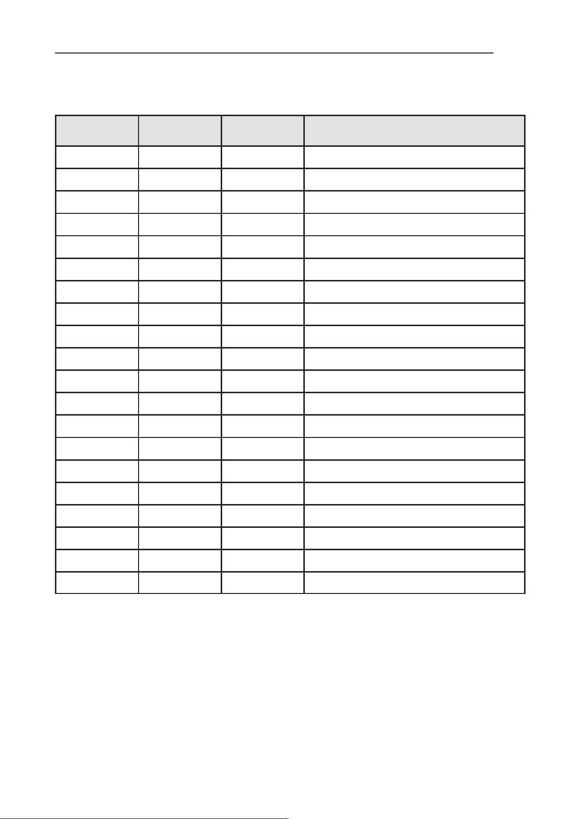
Figure 1. Remove the cover label from the front cover assembly
Page 11 – 4
Figure 2. Remove the 2 pcs screws from the front cover assembly
Issue 1 06/01
Page 5
PAMS
RAE-3
Technical Documentation
11. Disassembly and Service Instructions
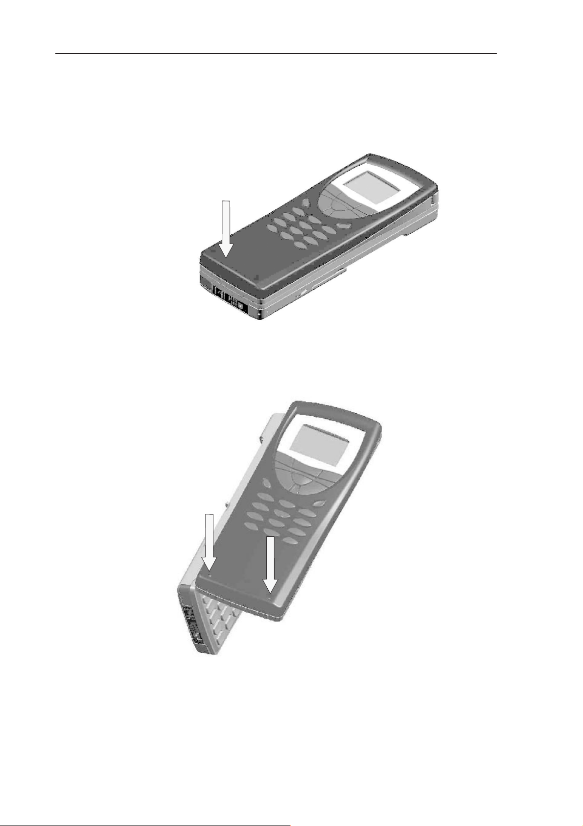
Figure 3. Remove the front cover assembly from the Screen frame.
Issue 1 06/01
Figure 4. Remove the CMT keymat from the UI module.
Page 11 – 5
Page 6
RAE-3
PAMS
1 1. Disassembly and Service Instructions
Technical Documentation
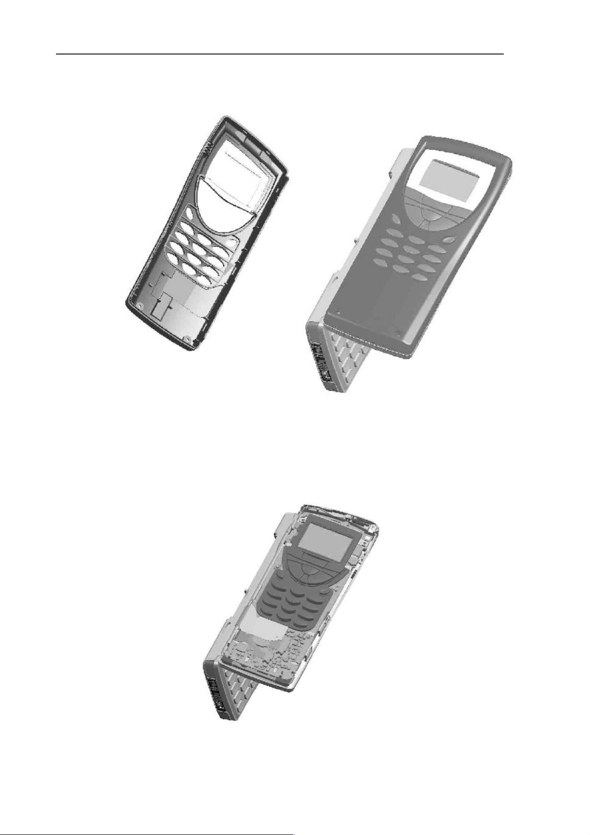
Figure 5. Remove the 2 screws from the Screen Frame.
Page 11 – 6
Figure 6. Remove the coaxial cable from the UI PWB.
Issue 1 06/01
Page 7

PAMS
RAE-3
Technical Documentation
11. Disassembly and Service Instructions
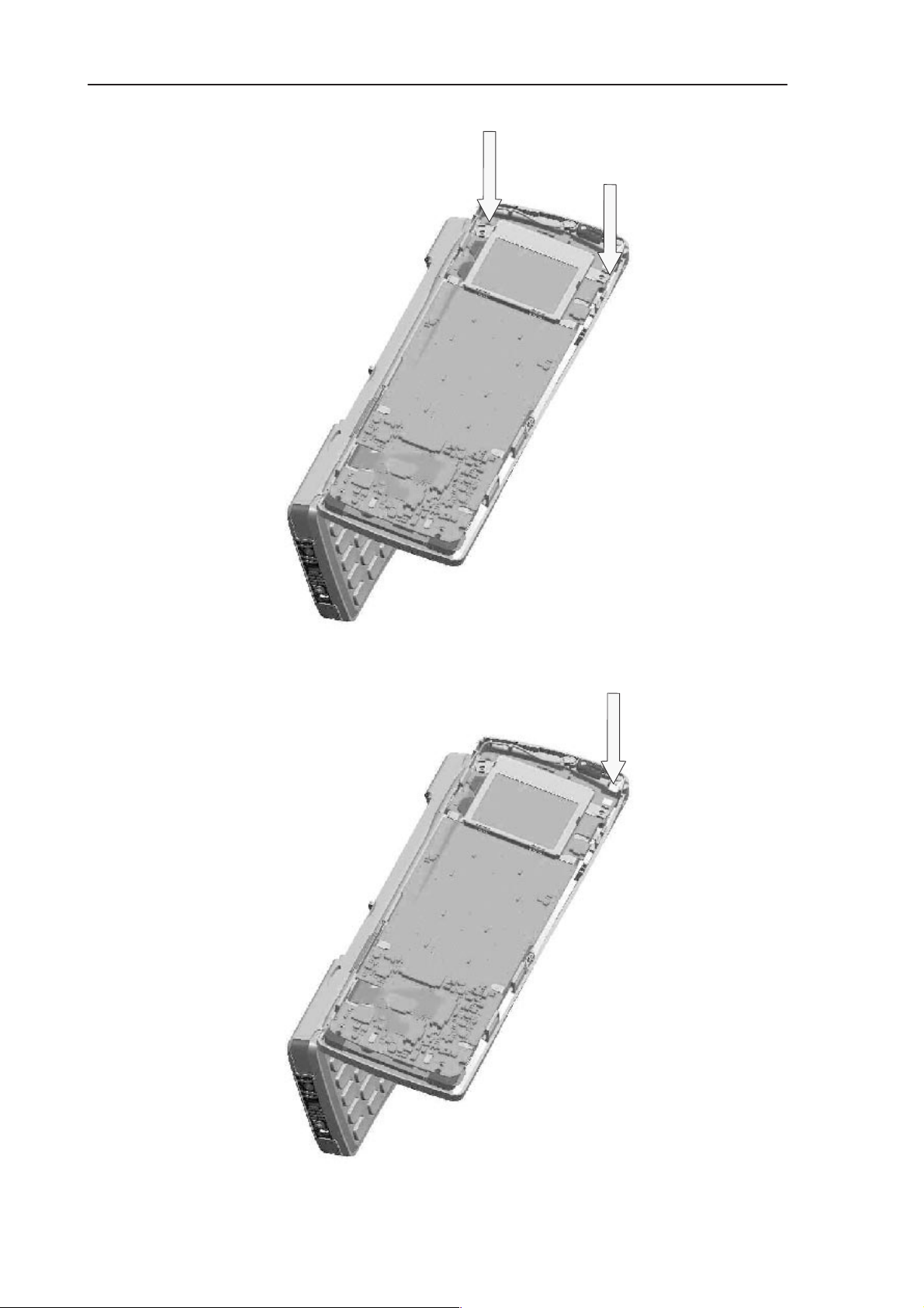
Figure 7. Remove the QWERTY flex from the UI PWB.
Issue 1 06/01
Figure 8. Remove the UI module from the Screen frame.
Page 11 – 7
Page 8

RAE-3
PAMS
1 1. Disassembly and Service Instructions
Technical Documentation
Figure 9. Remove the 4 plugs from the Back cover assembly.
Page 11 – 8
Figure 10. Remove the card cover from the Back cover assembly.
Issue 1 06/01
Page 9

PAMS
RAE-3
Technical Documentation
11. Disassembly and Service Instructions
Figure 11. Remove the 6 screws from the back cover assembly.
Issue 1 06/01
Figure 12. Remove the back cover assembly from the frame.
Page 11 – 9
Page 10

RAE-3
PAMS
1 1. Disassembly and Service Instructions
Technical Documentation
Figure 13. Remove the earpiece and its gasket from the audio holder assembly.
Page 11 – 10
Figure 14. Remove the battery latch from the audio holder assembly.
Issue 1 06/01
Page 11

PAMS
RAE-3
Technical Documentation
11. Disassembly and Service Instructions
Figure 15. Remove the extension of the QWERTY flex from the audio holder assembly.
Issue 1 06/01
Figure 16. Remove the audio holder assembly from the chassis assembly.
Page 11 – 11
Page 12

RAE-3
PAMS
1 1. Disassembly and Service Instructions
Technical Documentation
Figure 17. Remove the backup battery from BL8.
Page 11 – 12
Figure 18. Remove the coaxial cable from BL8.
Issue 1 06/01
Page 13

PAMS
RAE-3
Technical Documentation
11. Disassembly and Service Instructions
Figure 19. Remove the BL8 from Chassis assembly.
Figure 20. Remove the chassis assembly and the Qwerty flex UL8 from the frame.
Issue 1 06/01
Page 11 – 13
Page 14

RAE-3
PAMS
1 1. Disassembly and Service Instructions
Technical Documentation
Figure 21. Remove the QWERTY keymat from the frame.
Page 11 – 14
Figure 22. Frame assembly.
Issue 1 06/01
Page 15

PAMS
RAE-3
Technical Documentation
Test Points of BL8 module
11. Disassembly and Service Instructions
Figure 23. Top side test points
Issue 1 06/01
Figure 24. Bottom side test points
Page 11 – 15
Page 16

RAE-3
PAMS
1 1. Disassembly and Service Instructions
Table 1. System HW test points
Test point Signal PWB side Notes
J301 ExtSysResetX Bottom
J302 VCXOPWR Bottom
J303 SLEEPCLK Top Clk32k
J304 PURX Bottom
J305 CCONTINT Top
J306 PCMSClk Bottom
J307 PCMTxData Bottom
J308 PCMRxData Top
J309 PCMDClk Top
J310 SDRCLK Bottom
J311 SDRCKE Bottom
J312 SDRRASX Bottom
J313 SDRCASX Bottom
J314 SDRWEX Bottom
J315 SDRDQML Bottom
J316 SDRDQMU Bottom
J317 CCONTCSX Top
J318 GENSCLK Bottom
J319 SynthPWR Bottom
J320 TxPA Bottom
J321 COBBARSTX Bottom DSPGenOut0
J322 COBBACLK Bottom
J323 COBBACSX Bottom
J324 COBBASDa Bottom
J325 COBBAQDa Top
J326 COBBAIDa Bottom
J327 SEPClk Bottom
J328 SEPI Top
J329 SEP0 Bottom
J330 CoEmu0 Bottom
J331 CoEmu1 Bottom
J332 JTRst Bottom
J333 JTDI Bottom
J334 JTClk Bottom
J335 JTMS Bottom
J336 JTDO Bottom
J337 SEPCSX Top
J338 FLCS0X Bottom
J339 FLCS1X Bottom
J340 FLCS2X Bottom
J341 FLOEX Bottom
J342 FLWEX Bottom
Technical Documentation
Page 11 – 16
Issue 1 06/01
Page 17

PAMS
RAE-3
Technical Documentation
Table 1. System HW test points (continued)
J343 FLRPX Bottom
J346 SER_FL_RPY Bottom MPUGenIO2
J347 FLWPX Bottom MPUGenIO1
J348 SDRAd6 Bottom
J349 SDRDa8 Bottom
J350 FLAd5 Bottom
J351 FLDa7 Bottom
J500 SDATA Top SynthData, test point in RF sheet
J501 SCLK Top SynthClk, test point in RF sheet
J502 SENA1 Top SynthEna1X, test point in RF sheet
11. Disassembly and Service Instructions
NotesPWB sideSignalTest point
Issue 1 06/01
Page 11 – 17
Page 18

RAE-3
PAMS
1 1. Disassembly and Service Instructions
Technical Documentation
This page intentionally left blank.
Page 11 – 18
Issue 1 06/01
 Loading...