

Page 1

PAMS Technical Documentation
RAE-3 Series PDA
8. Troubleshooting
Issue 1 06/01
Copyright 2001. Nokia Mobile Phones. All Rights Reserved.
Page 2
RAE-3
PAMS
8. Troubleshooting
Amendment
Number
Date Inserted By Comments
06/01 OJuntunen
Technical Documentation
AMENDMENT RECORD SHEET
Page 8 – 2
Issue 1 06/01
Page 3

PAMS
RAE-3
Technical Documentation
CONTENTS –Troubleshooting
Introduction 8 – 6. . . . . . . . . . . . . . . . . . . . . . . . . . . . . . . . . . . . . . . . . . . .
RAE–3 System HW / UI Troubleshooting 8 – 6. . . . . . . . . . . . . . . .
Tools needed for troubleshooting: 8 – 6. . . . . . . . . . . . . . . . . . . .
General guidelines 8 – 6. . . . . . . . . . . . . . . . . . . . . . . . . . . . . . . . .
System HW / UI Troubleshooting Cases 8 – 8. . . . . . . . . . . . . . . . . . .
Nominal Current Consumption 8 – 9. . . . . . . . . . . . . . . . . . . . . . . . . . . .
1 System HW / UI Troubleshooting Cases 8 – 10. . . . . . . . . . . . . . . . . .
1.1 Dead Device 8 – 10. . . . . . . . . . . . . . . . . . . . . . . . . . . . . . . . . . . . .
1.2 Keypad problems 8 – 11. . . . . . . . . . . . . . . . . . . . . . . . . . . . . . . . .
2 BL8 System HW related 8 – 13. . . . . . . . . . . . . . . . . . . . . . . . . . . . . . . .
2.1 Flash programming troubleshooting 8 – 13. . . . . . . . . . . . . . . . .
2.1.1 Flashing does not start 8 – 13. . . . . . . . . . . . . . . . . . . . . . . . .
2.1.2 Flash memory fault indicated 8 – 14. . . . . . . . . . . . . . . . . . .
2.1.3 Flash VPP Error 8 – 15. . . . . . . . . . . . . . . . . . . . . . . . . . . . . .
2.1.4 Flash Erasing /Programming Error 8 – 16. . . . . . . . . . . . . . .
2.2 General Power Checking 8 – 17. . . . . . . . . . . . . . . . . . . . . . . . . . .
2.3 Device does not stay ON 8 – 19. . . . . . . . . . . . . . . . . . . . . . . . . . .
2.4 Charging checking 8 – 20. . . . . . . . . . . . . . . . . . . . . . . . . . . . . . . .
2.5 Backup Battery 8 – 22. . . . . . . . . . . . . . . . . . . . . . . . . . . . . . . . . . .
2.5.1 Backup battery troubleshooting 8 – 22. . . . . . . . . . . . . . . . .
2.6 Accessory Power Output Troubleshooting 8 – 24. . . . . . . . . . . .
2.6.1 No Accessory Voltage when needed 8 – 25. . . . . . . . . . . . .
2.6.2 Accessory Voltage ON all the time 8 – 26. . . . . . . . . . . . . . .
2.7 Clocks 8 – 27. . . . . . . . . . . . . . . . . . . . . . . . . . . . . . . . . . . . . . . . . . .
2.7.1 Clocks Troubleshooting 8 – 27. . . . . . . . . . . . . . . . . . . . . . . .
2.8 Memory Tests 8 – 29. . . . . . . . . . . . . . . . . . . . . . . . . . . . . . . . . . . .
2.8.1 Test in boot up 8 – 29. . . . . . . . . . . . . . . . . . . . . . . . . . . . . . . .
2.8.2 Test in PTS/WinTesla flashing 8 – 30. . . . . . . . . . . . . . . . . . .
2.9 Memory Troubleshooting 8 – 31. . . . . . . . . . . . . . . . . . . . . . . . . . .
2.9.1 Memory fails In Boot Up tests 8 – 31. . . . . . . . . . . . . . . . . . .
2.9.2 CMT display backlight blinking 2 times in a loop 8 – 32. . .
2.9.3 CMT display backlight blinking 3 times in a loop 8 – 33. . .
2.9.4 CMT display backlight blinking 4 times in a loop 8 – 36. . .
2.9.5 Memory fails in PTS/WinTesla flashing 8 – 38. . . . . . . . . . .
2.9.6 Serial Flash id read test fails 8 – 40. . . . . . . . . . . . . . . . . . . .
2.10 Serial Interface Troubleshooting 8 – 41. . . . . . . . . . . . . . . . . . . .
2.11 CONTACT SERVICE in CMT display 8 – 44. . . . . . . . . . . . . . .
2.12 CCONT Serial interface Troubleshooting 8 – 46. . . . . . . . . . . .
2.13 SIM Card 8 – 48. . . . . . . . . . . . . . . . . . . . . . . . . . . . . . . . . . . . . . .
2.13.1 SIM Card Error Troubleshooting 8 – 48. . . . . . . . . . . . . . .
2.13.2 SIM Card Rejected 8 – 49. . . . . . . . . . . . . . . . . . . . . . . . . . .
8. Troubleshooting
Page No
Issue 1 06/01
Page 8 – 3
Page 4

RAE-3
PAMS
8. Troubleshooting
2.13.3 Insert SIM card 8 – 51. . . . . . . . . . . . . . . . . . . . . . . . . . . . . .
2.14 Memory Card 8 – 53. . . . . . . . . . . . . . . . . . . . . . . . . . . . . . . . . . . .
2.14.1 Memory Card Interface Troubleshooting 8 – 53. . . . . . . .
2.14.2 Memory card switch troubleshooting: 8 – 55. . . . . . . . . . .
2.15 Lid Switch 8 – 56. . . . . . . . . . . . . . . . . . . . . . . . . . . . . . . . . . . . . . .
2.15.1 Lid Switch Troubleshooting 8 – 56. . . . . . . . . . . . . . . . . . . .
2.16 Battery Removal Switch troubleshooting 8 – 58. . . . . . . . . . . .
2.17 COBBA Control Interface troubleshooting 8 – 60. . . . . . . . . . .
2.18 COBBA PCM Interface Troubleshooting 8 – 62. . . . . . . . . . . . .
2.19 Audio troubleshooting 8 – 65. . . . . . . . . . . . . . . . . . . . . . . . . . . .
2.19.1 Both Mic and Earpiece/PHF faulty 8 – 65. . . . . . . . . . . . . .
2.19.2 Mic faulty 8 – 67. . . . . . . . . . . . . . . . . . . . . . . . . . . . . . . . . . .
2.19.3 Earpiece faulty 8 – 68. . . . . . . . . . . . . . . . . . . . . . . . . . . . . . .
2.19.4 PHF Speaker faulty 8 – 69. . . . . . . . . . . . . . . . . . . . . . . . . .
2.19.5 Headset out of order 8 – 71. . . . . . . . . . . . . . . . . . . . . . . . . .
2.20 RF Interface 8 – 73. . . . . . . . . . . . . . . . . . . . . . . . . . . . . . . . . . . . .
2.20.1 Phone doesn’t register to the network l 8 – 73. . . . . . . . . .
2.21 IR Interface Troubleshooting diagram 8 – 74. . . . . . . . . . . . . . .
2.22 BL8 related Keyboard problems 8 – 75. . . . . . . . . . . . . . . . . . . .
2.23 BL8 related PDA UI problems 8 – 79. . . . . . . . . . . . . . . . . . . . . .
2.24 BL8 related CMT UI problems 8 – 84. . . . . . . . . . . . . . . . . . . . .
Technical Documentation
3 DL2 UI Troubleshooting 8 – 86. . . . . . . . . . . . . . . . . . . . . . . . . . . . . . . .
3.1 CMT and keypad illumination problems 8 – 86. . . . . . . . . . . . . .
3.2 CMT LCD Troubleshooting 8 – 86. . . . . . . . . . . . . . . . . . . . . . . . .
3.3 No picture on PDA LCD or picture is faulty 8 – 87. . . . . . . . . . . .
3.4 Backlight troubleshooting 8 – 100. . . . . . . . . . . . . . . . . . . . . . . . . . .
3.5 DL2 related keyboard problems 8 – 105. . . . . . . . . . . . . . . . . . . . .
4 UL 8 FLEX related 8 – 106. . . . . . . . . . . . . . . . . . . . . . . . . . . . . . . . . . . . .
4.1 Audio troubleshooting 8 – 106. . . . . . . . . . . . . . . . . . . . . . . . . . . . . .
4.2 Display problem 8 – 107. . . . . . . . . . . . . . . . . . . . . . . . . . . . . . . . . . .
4.3 Battery Removal Switch problem 8 – 108. . . . . . . . . . . . . . . . . . . .
4.4 UL8 related keyboard problems 8 – 108. . . . . . . . . . . . . . . . . . . . .
5 RF related 8 – 109. . . . . . . . . . . . . . . . . . . . . . . . . . . . . . . . . . . . . . . . . . . .
Introduction to troubleshooting 8 – 109. . . . . . . . . . . . . . . . . . . . . . .
RF Key Component Placement 8 – 110. . . . . . . . . . . . . . . . . . . . . .
5.1 EGSM Receiver 8 – 111. . . . . . . . . . . . . . . . . . . . . . . . . . . . . . . . . . .
General Instructions for troubleshooting 8 – 111. . . . . . . . . . . . . . .
5.1.1 Troubleshooting diagram for EGSM Receiver 8 – 112. . . . .
5.1.2 EGSM Signal Path 8 – 113. . . . . . . . . . . . . . . . . . . . . . . . . . . .
5.1.3 RX/TX Switch 8 – 113. . . . . . . . . . . . . . . . . . . . . . . . . . . . . . . . .
5.1.4 Front end 8 – 113. . . . . . . . . . . . . . . . . . . . . . . . . . . . . . . . . . . .
5.1.5 Hagar 8 – 114. . . . . . . . . . . . . . . . . . . . . . . . . . . . . . . . . . . . . . .
5.2 PCN Receiver 8 – 115. . . . . . . . . . . . . . . . . . . . . . . . . . . . . . . . . . . .
General Instructions for troubleshooting 8 – 115. . . . . . . . . . . . . . .
5.2.1 PCN Signal Path 8 – 117. . . . . . . . . . . . . . . . . . . . . . . . . . . . . .
Page 8 – 4
Issue 1 06/01
Page 5

PAMS
RAE-3
Technical Documentation
5.2.2 RX/TX Switch 8 – 117. . . . . . . . . . . . . . . . . . . . . . . . . . . . . . . . .
5.2.3 Front end 8 – 117. . . . . . . . . . . . . . . . . . . . . . . . . . . . . . . . . . . .
5.2.4 Hagar 8 – 117. . . . . . . . . . . . . . . . . . . . . . . . . . . . . . . . . . . . . . .
5.3 EGSM Transmitter 8 – 119. . . . . . . . . . . . . . . . . . . . . . . . . . . . . . . .
General troubleshooting instructions 8 – 119. . . . . . . . . . . . . . . . . .
5.3.1 Path of transmitted EGSM signal 8 – 119. . . . . . . . . . . . . . . .
5.3.2 Troubleshooting diagram for EGSM Transmitter 8 – 120. . .
5.4 PCN Transmitter 8 – 122. . . . . . . . . . . . . . . . . . . . . . . . . . . . . . . . . .
General troubleshooting instructions 8 – 122. . . . . . . . . . . . . . . . . .
5.4.1 Path of the transmitted PCN signal 8 – 122. . . . . . . . . . . . . .
5.4.2 Troubleshooting diagram for PCN Transmitter 8 – 123. . . . .
5.5 Synthesizer 8 – 125. . . . . . . . . . . . . . . . . . . . . . . . . . . . . . . . . . . . . .
General troubleshooting instructions 8 – 125. . . . . . . . . . . . . . . . . .
5.5.1 26 MHz reference oscillator ( VCTCXO ) 8 – 125. . . . . . . . .
5.5.2 VCO 8 – 125. . . . . . . . . . . . . . . . . . . . . . . . . . . . . . . . . . . . . . . .
5.5.3 Troubleshooting diagram for PLL Synthesizer 8 – 126. . . . .
5.5.4 PLL Block Diagram 8 – 128. . . . . . . . . . . . . . . . . . . . . . . . . . . .
5.6 Frequency lists 8 – 129. . . . . . . . . . . . . . . . . . . . . . . . . . . . . . . . . . .
8. Troubleshooting
6 Diagrams of Test Points 8 – 143. . . . . . . . . . . . . . . . . . . . . . . . . . . . . . . .
Issue 1 06/01
Page 8 – 5
Page 6

RAE-3
PAMS
8. Troubleshooting
Introduction
This document is intend to be a guide for localizing and repairing electrical
faults in the RAE–3 device. First there is a brief guide for fault localizing. Then
fault repairing is divided into troubleshooting paths.
Before any service operation you must be familiar with the RAE-3 product and
module level architecture. You must also be familiar with the RAE-3 specified
service tools such as the WinTesla service software, Flashing tools and software. Basic skills of using RF measurement devices are required when starting
to follow the RF troubleshooting paths.
RAE–3 System HW / UI Troubleshooting
Tools needed for troubleshooting:
S Service tools defined in RAE–3 manual “Service Tools” section
S Laboratory power supply with current indicator
S Oscilloscope
Technical Documentation
S Digital multimeter . .
General guidelines
General notes about the RAE–3 product:
S RAE–3 has only one common engine – BL8 system HW, . . . .
comprising CMT (phone) and PDA (computer). . . . .
S There are separate CMT and PDA displays and keyboards
S CMT display/keyboard and PDA display are on the UI module
DL2. . . . .
S PDA QWERTY–keyboard UI is on UL8 flex module
S Audio connections for the handsfree speaker and earpiece are
on the UL8 flex module. . . . .
When you have a faulty RAE-3 device and you start to troubleshoot it, check
first the following items:
S If the RAE-3 cannot be turned on by any means, see ”dead . .
device” troubleshooting. . . . .
S Blinking CMT display means that a memory fault is preventing
normal boot up (–> Memory tests). . . . .
Page 8 – 6
S Current consumption (missing consumption) gives an idea . . .
whether the device able to start up. . . . .
S Dropping supply voltage indicates a short circuit
S Check whether the connection with Wintesla works and what can
be discovered with Wintesla. . . . .
S Check self tests with Wintesla if ”CONT ACT SERVICE” is shown
on the CMT display. . . . .
Issue 1 06/01
Page 7

PAMS
RAE-3
Technical Documentation
S Check visual display faults
S Check that all connectors make good contacts
– this might be the problem if the displays are dark or partially dark or if there
are keyboard problems.
Locate failed module (BL8, UL8, DL2) with the MJS–14 test jig.
This is the basis of further troubleshooting.
S Check the failed module(s) visually:
– mechanical damages?
– solder joints OK?
Continue with the specific troubleshooting procedure for the module:
S If there is an obvious fault, repair it before reflashing the device
S Flash first if a fault is not obvious
– Flashing troubleshooting leads to power checking and serial interface
checking if flashing does not start.
– At the beginning of flash programming, all memory interfaces are first
tested
– If flashing is aborted and error(s) return, refer to Memory testing section.
8. Troubleshooting
Due to CSP packages short–circuits or broken solder joints are not easily seen.
If the examined signal seems to be continuously in low or high level, then measure for possible short–circuit to ground (signal low) or to supply voltage (signal
high). Note that if a problem is not found from any visible contact/component it
can be under the CSPs where the signal is connected.
If there is no short circuit and the signal level is continuously at a low level, then
the following faults are possible:
– contact problem in output soldering (output active)
– contact problem in soldering of pin having internal pull–up (tri–stated signals)
Care must be taken when assembling and disassembling the transceiver. Refer to the instructions in this manual. Failure to do this may result in unnecessary damage to the device.
The PDA display must be calibrated after the following actions have been taken:
– RAE–3 has been flashed
– PDA display or DL2 module has been replaced
Note:
set the RTC running time to 10 hours.
– Service battery BBL-3B does that automatically.
– Always use only the BBL-3B service battery with Wintesla.
The last step in service before returning the RAE-3 to the customer is to
Issue 1 06/01
Page 8 – 7
Page 8

RAE-3
PAMS
8. Troubleshooting
Technical Documentation
System HW / UI Troubleshooting Cases
1. Troubleshooting of System HW/UI is divided to following cases:
1.1 Dead Device. . . . . . . .
1.2 Keypad problem. . . . . . . .
2. BL8 System HW related:
2.1 Flash programming troubleshooting. . . . . . . .
2.2 General Power Checking. . . . . . . .
2.3 Device does not stay ON. . . . . . . .
2.4 Charging checking. . . . . . . .
2.5 Backup Battery. . . . . . . .
2.6 Accessory Power Output Troubleshooting. . . . . . . .
2.7 Clocks. . . . . . . .
2.8 Memory Tests. . . . . . . .
2.9 Memory Troubleshooting. . . . . . . .
2.10 Serial Interface Troubleshooting. . . . . . . .
2.11 CONTACT SERVICE in CMT display. . . . . . . .
2.12 CCONT Serial interface Troubleshooting. . . . . . . .
2.13 SIM Card. . . . . . . .
2.14 Memory Card. . . . . . . .
2.15 Lid Switch. . . . . . . .
2.16 Battery Removal Switch troubleshooting. . . . . . . .
2.17 COBBA Control Interface troubleshooting. . . . . . . .
2.18 COBBA PCM Interface Troubleshooting. . . . . . . .
2.19 Audio troubleshooting. . . . . . . .
2.20 RF Interface. . . . . . . .
2.21 IR Interface Troubleshooting diagram. . . . . . . .
2.22 BL8 related Keyboard problems. . . . . . . .
2.23 BL8 related PDA UI problems. . . . . . . .
Page 8 – 8
2.24 BL8 related CMT UI problems. . . . . . . .
3. DL2 UI Related:
3.1 CMT and keypad illumination problems. . . . . . . .
3.2 CMT LCD Troubleshooting. . . . . . . .
3.3 No picture on PDA LCD or picture is faulty. . . . . . . .
3.4 Backlight troubleshooting. . . . . . . .
3.5 DL2 related keyboard problems. . . . . . . .
Issue 1 06/01
Page 9
PAMS
RAE-3
Technical Documentation
4. UL8 Flex Related:
4.1 Audio troubleshooting. . . . . . . .
4.2 Display problem. . . . . . . .
4.3 Battery Removal Switch problem. . . . . . . .
4.4 UL8 related keyboard problems. . . . . . . .
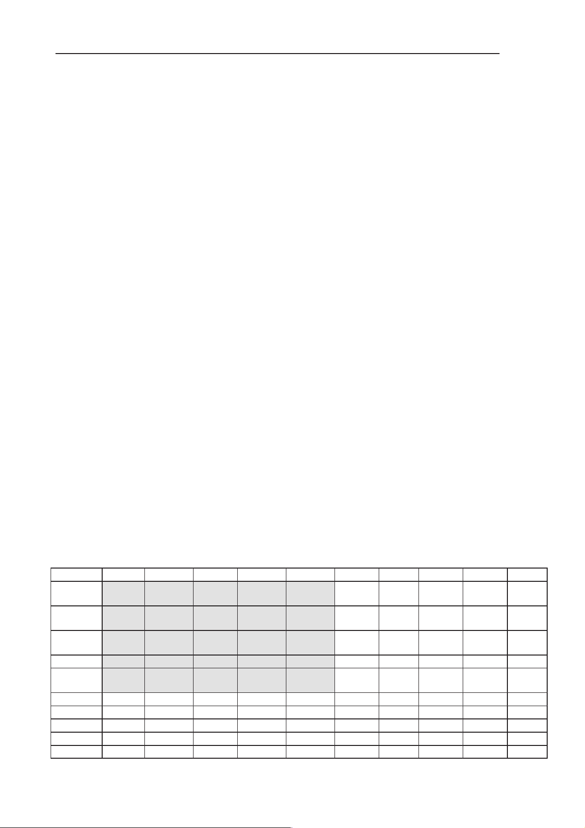
Nominal Current Consumption
The following power consumption values (ref.Table 1 ) are measured from a
complete RAE-3.
Vbattery = 3.7 V.
Measured nominal currents are drawn from the main battery.
Measurements have been made with a current proble connected to an oscillo-
scope.
Table 1. Nominal current consumption in different operating modes
8. Troubleshooting
State CMT OFF CMT ON 2W Call (TX5) 0.2W Call (TX19)
Lid closed 2.4 mA 5.6 mA 310 mA
(Voice call)
Lid Open
(min. brightness
on PDA display)
Lid Open
(max. brightness
on PDA display)
60 mA (running) 65 mA (running) 365 mA
(HF call)
140 mA (running) 145 mA (running) 445 mA
(HF call)
120 mA
(Voice call)
170 mA
(HF call)
255 mA
(HF call)
Identify the failed module (UL8, DL2, BL8) using the MJS–19 jig.
Issue 1 06/01
Page 8 – 9
Page 10
RAE-3
PAMS
8. Troubleshooting
Technical Documentation
1 System HW / UI Troubleshooting Cases
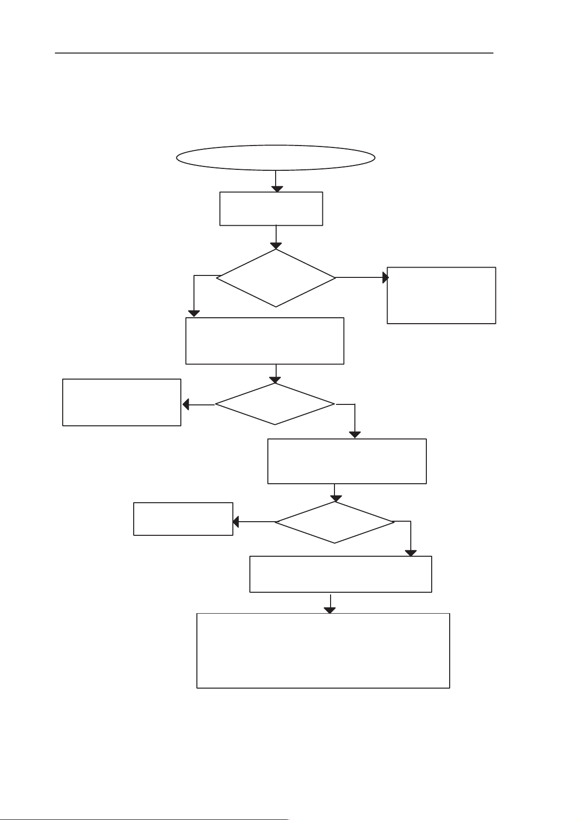
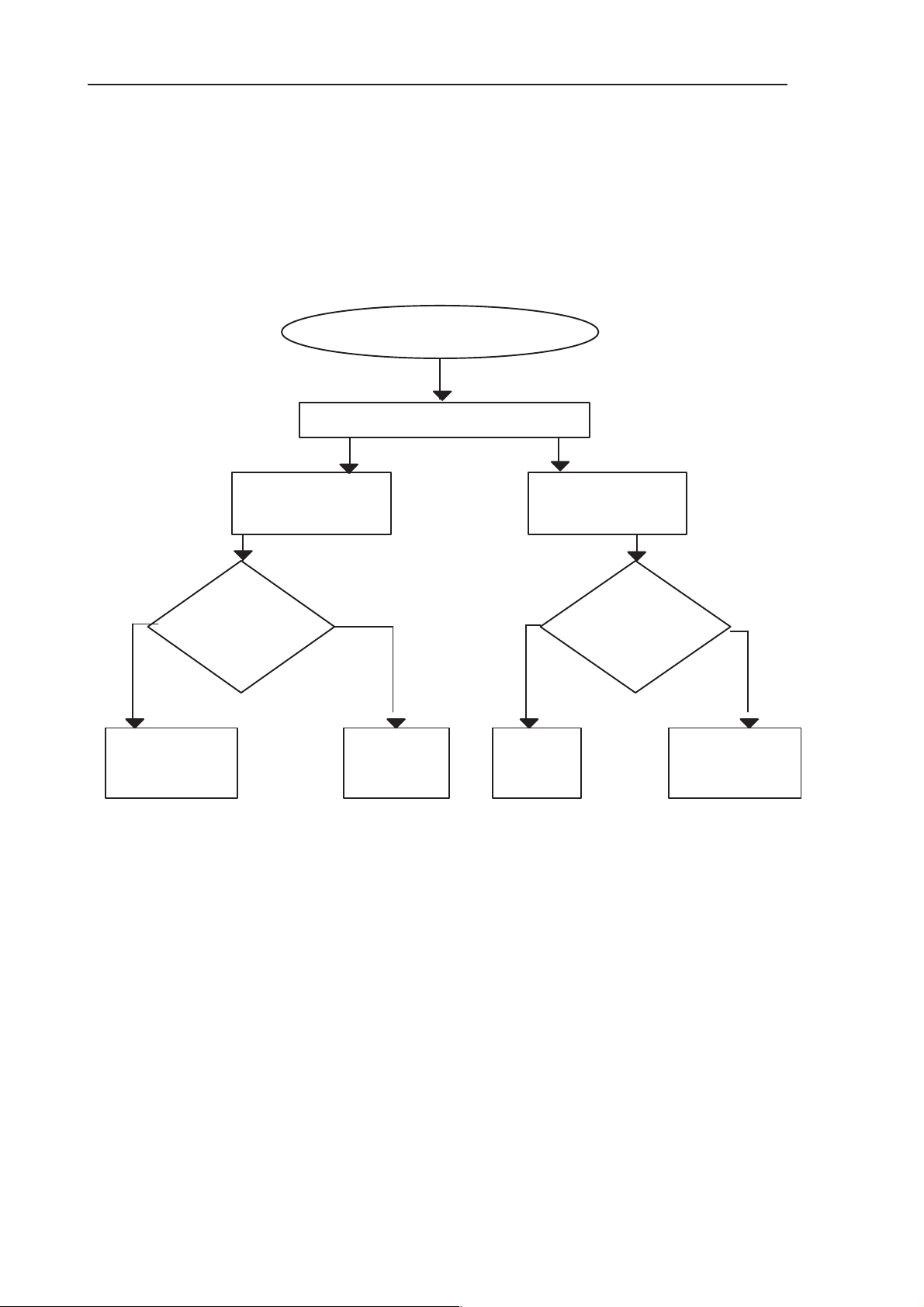
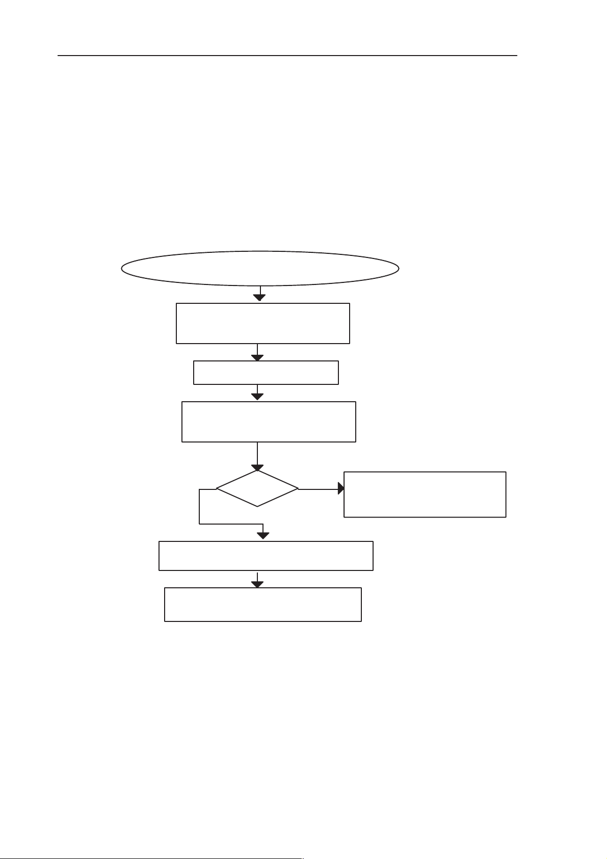
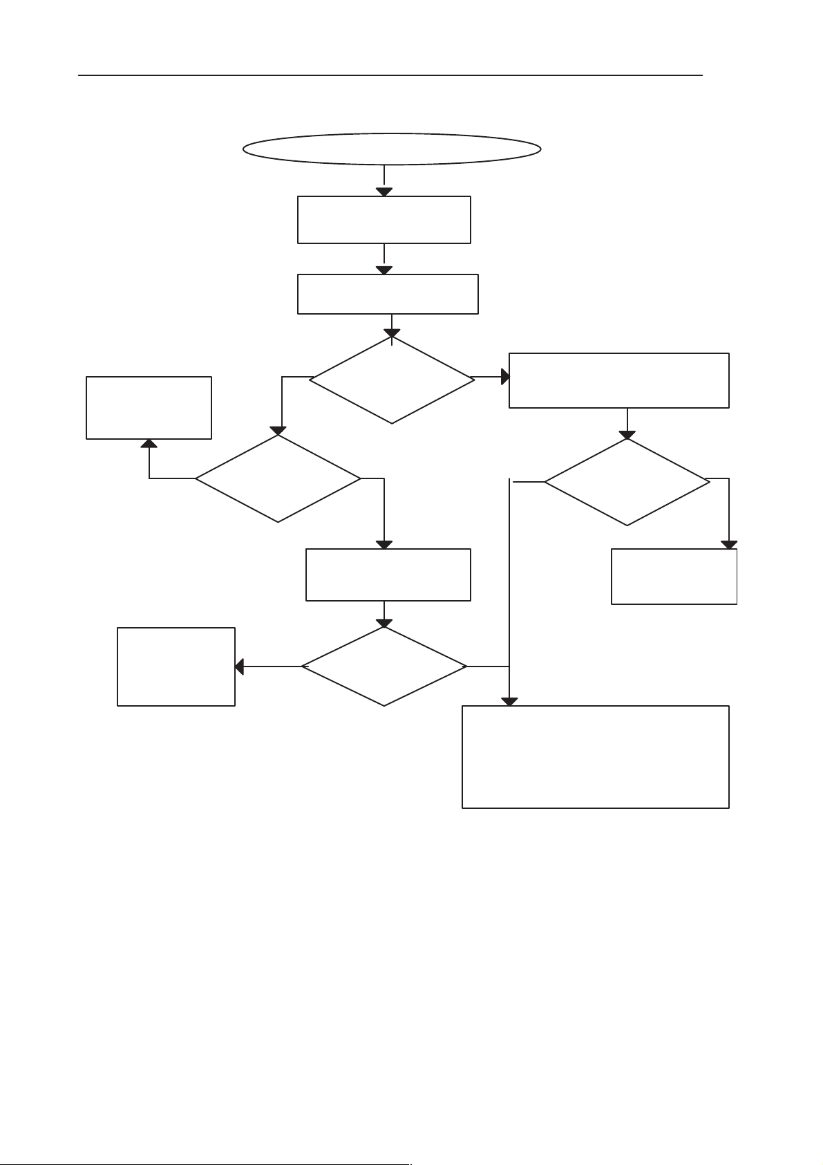
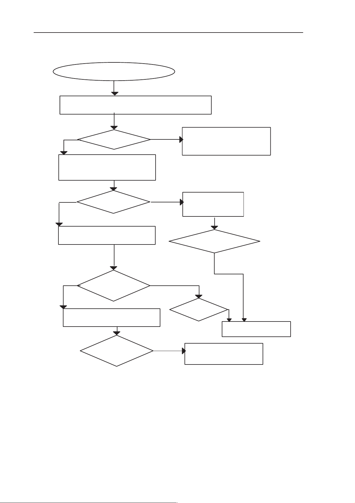
1.1 Dead Device
Dark display
Check
supply voltage
NO
Supply
voltage
drops ?
Check
YES
Go to General
Power Checking
(short circuit
possible)
Go to Flashing
troubleshooting/
general power check
NO
Replace
defective
connector
serial connection with WinTesla
OK?
Check connectors
BL8/UL8, UL8/DL2, DL2/displays
NO
UI related troubleshooting of failed module:
– BL8 related CMT UI troubleshooting (BL8 failed)
– BL8 related PDA UI troubleshooting (BL8 failed)
– CMT LCD troubleshooting (DL2 failed)
– No picture/faultly picture on PDA LCD (DL2 failed)
– PDA backlight troubleshooting (DL2 failed)
– UL8 keyboard module troubleshooting (UL8 failed)
Connectors
Identify failed module
(BL8, UL8, DL2)
with MJS-14 jig
YES
YES
OK ?
Go to
Page 8 – 10
Figure 1.
Issue 1 06/01
Page 11
PAMS
RAE-3
Technical Documentation
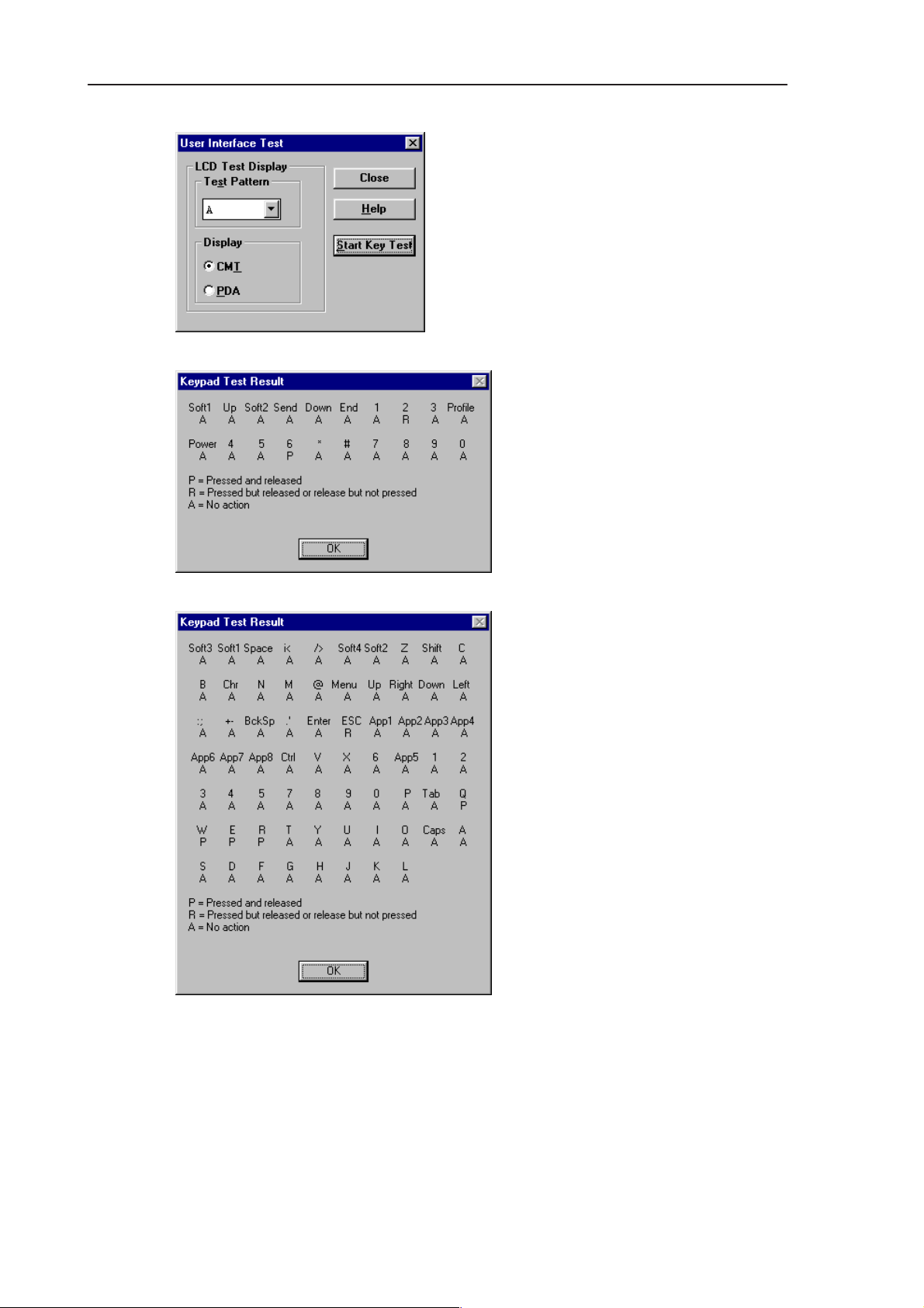
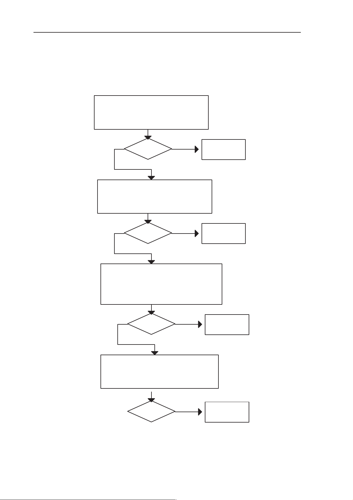
1.2 Keypad problems
1. Connect the phone under test to Wintesla.
2. Select Testing –> User interface testing
3. Select the CMT to be tested from the ”Display” panel and click ”Start
key test” (figure 1). The test starts and the button text changes to ”Stop key
test”.
4. Click the ”Stop key test”. Result window (Figure 2) appears.
All letters under the key names should show ”A”. . . . . . . . .
If there is ”R”, the key is stuck. . . . . . . . .
Repeat the test. If the result is the same, use table 1 to find out the signals connected to the particular key(s).
5. Click ”Start key test” again.
This time, press and release all keys through, then stop the test. . . . . . . . .
There should be ”P” for every key. . . . . . . . .
If ”A” results are seen, repeat and press these keys again. If key. . . . . . . .
presses are not registered, find out the signals connected to the key.
6. Change the keypad to be tested to PDA. Repeat test steps 4 and 5
for the PDA keyboard. The result window is shown in Figure 3.
8. Troubleshooting
7. Open the CMT side cover. Check the 50–way connector on UL2.
Is it properly inserted, both parts of the connector properly soldered?. . . . . . . .
Repair, retest
8. Check CMT key mat alignment and membrane switches on the mat.
Replace key mat if broken.
9. Check 70–way connector on BL8.
Is it properly inserted, both parts of the connector properly soldered?. . . . . . . .
Repair, retest
10. Locate the faulty part by placing the parts into service jig and chang-
ing the parts one by one. Follow instructions in the proper section (2.23 for BL8
fault, 4.4 for UL8 flex fault, 3.5 for UL2 display module fault).
Table 1. Keyboard matrix (keys on UL2 module highlighted) – English keymat
Col0 Col1 Col2 Col3 Col4 Col5 Col6 Col7 Col8 Col9
Row0 cmt
Soft1
Row1 cmt
Send
Row2 cmt 1 cmt 2 cmt 3 cmt
Row3 cmt 4 cmt 5 cmt 6 cmt * cmt # Menu Up Right Down Left
Row4 cmt 7 cmt 8 cmt 9 cmt 0 :; +– Back-
Row5 ESC App1 App2 App3 app4 App6 App7 App8
Row6 Ctrl V X 6 App5
Row7 1 2 3 4 5 7 8 9 0 P
Row8 Tab Q W E R T Y U I O
Row9 Caps A S D F G H J K L
cmt
Up
cmt
Down
cmt
Soft2
cmt
End
pda
Soft 3
pda
Soft 4
Profile
pda
Soft 1
pda
Soft 2
cmt
Power
Space Info < / >
Z Shift C B
Chr N M , @
Enter
space
Issue 1 06/01
Page 8 – 11
Page 12
RAE-3
PAMS
8. Troubleshooting
Technical Documentation
Figure 2. User interface test dialog
Figure 3. CMT keypad test results
Figure 4. PDA keypad test results
Page 8 – 12
Issue 1 06/01
Page 13
PAMS
RAE-3
Technical Documentation
2 BL8 System HW related
2.1 Flash programming troubleshooting
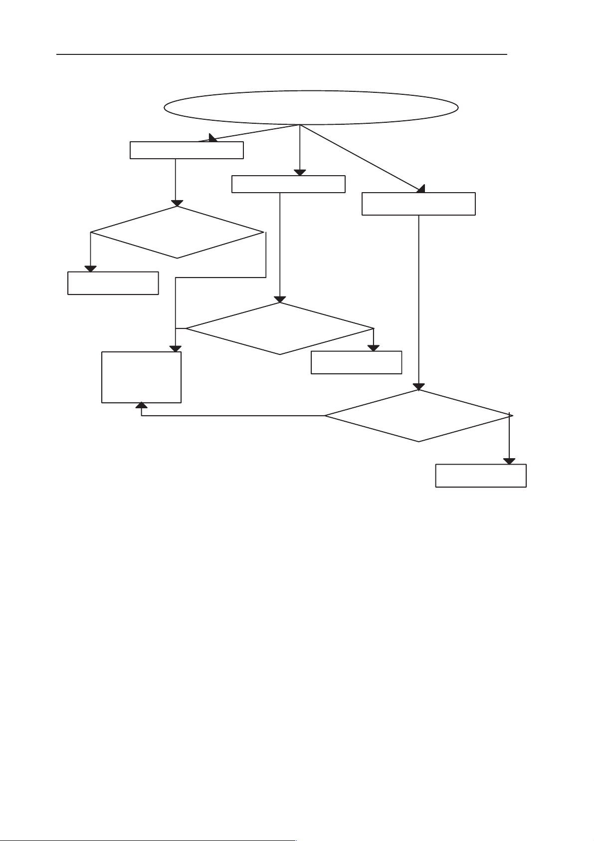
2.1.1 Flashing does not start
FLASH programming does not work
YES
If the fault information from the prommer is:
a) The Phone does not set Flashbus TXD line high after the startup
b) The Phone does not set Flashbus TXD line low after the line has been high. The Prommer generates this error also when the Phone is not connected to the Prommer.
c) The Phone MCU has not received the first dummy word correctly from the Prommer after the startup
d) The Phone has not received Secondary code bytes correctly
e) The Phone MCU can not start Secondary code correctly
OK
Check that Flashing equipment are functional and properly connected
8. Troubleshooting
YES
a) C138 VBB 2.8 V,
b) J304 (PURX) = ’1’ (= 2.8V)
c) J303 (SLEEPCLK) 32 kHz square wave
d) C303 13 MHz sine wave
Note: testpoints are explained more detailed in General Power
Checking – section
YES
Check that following lines are correct:
a) AccTxData line
b) AccRxData line
c) MBUS
Note: testpoints are explained more detailed in Serial
Interface troubleshooting – section
Figure 5.
NO
Jump to General Power
Checking
Powers OK
Jump to Clocks
Troubleshooting
NO
Jump to Serial Interface
troubleshooting
Issue 1 06/01
Page 8 – 13
Page 14
RAE-3
PAMS
8. Troubleshooting
2.1.2 Flash memory fault indicated
FLASH programming does not work
If the fault information from the prommer is:
a) The flash manufacturer and the device IDs in the existing Algorithm files do
not match with the IDs received from the phone.
b) The External RAM test failed in the Phone.
c) The Phone does not send acknowledge signal (ie. drop the Flashbus TXD
line to low state) after the Prommer has sent the Algorithm code.
d) The Prommer has detected a wrong ID byte in the MCU_ID_RESPONSE
message, which it has received from the Phone. See Note.
Technical Documentation
YES
YES
YES
YES
Jump to Memory Tests
Figure 6.
Note: Wintesla shows the following Flash ID’s for every flash device when
programming is going on.
If Flash ID bytes are correct the following bytes are shown:
Flash ID 0089–8896, 0089–8896, 0089–8896, 0000–0030
=Flash 0 =Flash 1 =Flash 2 = SF
But if one or more of Flash ID bytes is/are wrong the Flash is faulty or there is
short circuit in the flash interface.
Page 8 – 14
Issue 1 06/01
Page 15
PAMS
RAE-3
Technical Documentation
2.1.3 Flash VPP Error
FLASH programming does not work
If the fault information from the prommer is:
a) The erasing status response from the Phone informs about fail. The Prommer copies the
Phone response contents to the preceeding FIASCO_GENERAL_INFO_IND message.
b) The Prommer measures the PPD voltage level at flashing start. If the level is below the limit
the Prommer returns the corresponding error code.*
c) The programming status response from the Phone informs about fail.
The Prommer copies the phone response contents to the preceding FIASCO_GENERAL_
INFO_IND message
Note: A new error message will be shown with next coming Wintesla RAE–3 dll release
Check that UL8 flex connector is properly connected to Board to board connector on BL8
(=X400) ; (pins 15 (FLVPP) and 16 (PROG_EN) are connected in UL8 flex)
OK
YES
YES
8. Troubleshooting
* The VPP voltage level limit is 3 to 5 per cent below
the set VPP voltage level.
Check FLVPP voltage level
(= 2.8 V) during programming. (See Memory tests measurement points C368)
Note: By default tested with known good UL8 flex
NOT OK
Faulty UL8 Flex
Check voltage from Board to board adapter JC4
OK
connector pin 16 (= 2.8 V)
Note: By default tested with known good UL8 flex.
NOT OK
Check that UL8 Flex connector (=X12) is not broken and flex is OK.
Note: By default tested with known BL8 module.
OK
Wintesla informs which memory address the erasing fails. See note which
address corresponds which Flash components.
Erasing/programming fails
Faulty components D351, D352 or D353
NO
Check BL8’s
connector
X400
OK
Faulty MADLinda D300
(DSPGenOut2)
Note:
Flash 0 (=D351) erasing area starts 0x00000000
Flash 0 (=D351) erasing area stops 0x003FFFFF
Flash 1 (=D352) erasing area starts 0x01000000
Flash 1 (=D352) erasing area stops 0x013FFFFF
Issue 1 06/01
Note:
Flash 2 (=D353) erasing area starts 0x02000000
Flash 2 (=D353) erasing area stops 0x023FFFFF
Serial Flash (=D354) erasing area starts 0x8000000
Serial Flash (=D354) erasing area stops 0x841FFFF
Figure 7.
Page 8 – 15
Page 16
RAE-3
PAMS
8. Troubleshooting
2.1.4 Flash Erasing /Programming Error
FLASH programming does not work
If the fault information from the prommer is:
a) The erasing status response from the Phone informs about failure.
The Prommer copeies the contents of the response of the Phone into the
preceeding FIASCO_GENERAL_INFO_IND message.
b) The Phone has generated a NAK signal during data block transfer.
c) The programming status response from the Phone informs about failure.
The Prommer copies the contents of the response of the Phone into the
preceeding FIASCO_GENERAL_INFO_IND message.
Technical Documentation
YES
YES
Wintesla informs which memory address the erasing fails. See note which address
corresponds which Flash components.
Erasing/Programming fails
Change faulty flash D351, D352, D353 or D354
Note:
Flash 0 (=D351) erasing area starts 0x00000000
Flash 0 (=D351) erasing area stops 0x003FFFFF
Flash 1 (=D352) erasing area starts 0x01000000
Flash 1 (=D352) erasing area stops 0x013FFFFF
Flash 2 (=D353) erasing area starts 0x02000000
Flash 2 (=D353) erasing area stops 0x023FFFFF
Serial Flash (=D3534 erasing area starts 0x8000000
Serial Flash (=D3534 erasing area stops 0x841FFFF
Page 8 – 16
Figure 8.
Issue 1 06/01
Page 17
PAMS
RAE-3
Technical Documentation
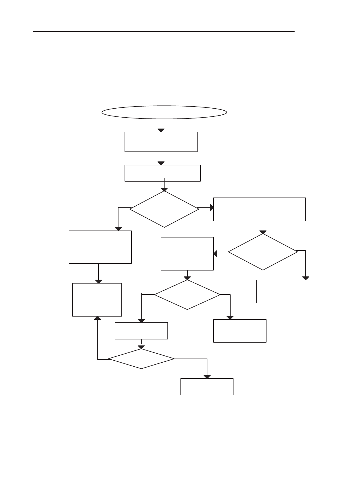
2.2 General Power Checking
Use BBL-3B service battery. Battery voltage must be 3.7 V.
Switch power
on
Supply voltage drops
when the power is
switched on
NO
VB (C124) and
VB_CCONT
(C115) 3.7V?
NO
YES
Failure in battery line
Check L100, L101 and
8. Troubleshooting
Short circuit in VBAT, VBB or VCORE line.
Switch power off and measure with multimeter which
of these voltages have a short circuit. Check visually
components which are connected to short circuited
voltage line.
X100
YES
PURX (J304) 2.8V
&
SLEEPCLK (J303)
32kHz
(typ. 32.768kHz)?
YES
VBB (C138)
2.8V?
YES
NO
NO
Remove
&
Insert service
battery
V2V (C140)
2.65V?
NO
Faulty circuit
N100, C140 or
R104
YES
Pin 5 of N102
V108 or R105
Drain of V106 low
around 60–100ms
when battery inserted
(FIg. 10)
YES
Faulty circuit N100 or
faulty 32kHz clock circuit
(B100, C120, C121, C122,
R113, R114 or R115)
YES
0V?
NO
Faulty circuit
NO
D101, D102,
V106, R102,
R108 or V102
N100
Faulty circuit
N102, C138 or
C111
Faulty circuit
VCORE (C119)
1.8V?
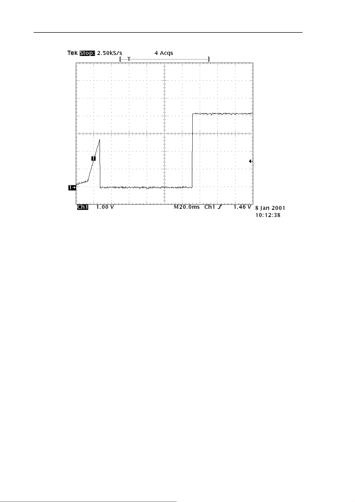
Oscilloscope screen shot (Figure 10) .
Issue 1 06/01
Faulty circuit L102, C131,
NO
V105, R118, L103, V104,
R116, R119, C118, C119
Figure 9.
Page 8 – 17
Page 18
RAE-3
PAMS
8. Troubleshooting
Technical Documentation
Figure 10. Drain of V106 when battery is inserted
Page 8 – 18
Issue 1 06/01
Page 19

PAMS
RAE-3
Technical Documentation
2.3 Device does not stay ON
If the device is switched off without any visible reason, there may be problems
in the following areas:
S CCONT watch dog problem
S BSI or BTEMP line problem
S Battery line problem
S Soldering problem
The most likely reason is CCONT WD (watchdog) problem, which turns the device off after about 32 s.
This may be caused by SW problem, MadLinda problem, CCONT problem or
memory problems.
The following tests are recommended:
S General Power Checking
8. Troubleshooting
S Clocks
S Memory testing
S CCONT serial interface
If there is something wrong in BSI and BTEMP lines, the device seems to be
dead after battery insertion. However, the regulators in the device are on 10s
before the powerdown.
This mode can easily be detected from the current consumption of the device.
After 10s the current consumption drops almost to 0mA.
In this case check components
C126, C127
R121, R122, R123,
C103, C104,
battery connector X100.
Issue 1 06/01
Page 8 – 19
Page 20

RAE-3
PAMS
8. Troubleshooting
2.4 Charging checking
Use the BLL–3 battery and the JBE-2 calibration unit to test charging.
When you are charging totally empty battery, remember that start–up charging
might take 2 minutes with ACP–9 charger and several minutes with ACP–7
charger.
During this time display is blank. If charger is not NMP approved type and supported by phone then the software doesn’t start charging and display ’NOT
CHARGING’.
Remove and reconnect battery and charger few times before you start to measure module. This check ensures if module fault really exists.
See the diagram Figure 11 next page.
Technical Documentation
Page 8 – 20
Issue 1 06/01
Page 21
PAMS
RAE-3
Technical Documentation
Display
information:
NOT
CHARGING
R121 voltage
is ~1.1V when charger is
connected
YES
R123 voltage
is ~0.5V when charger is
connected
YES
1Hz or 32Hz
square wave
(CHRG_CTRL) when charger
is connected *
NO
NO
NO
Check
BLL–3, BSI
resistor, X100,
R121, R122
Check
BLL–3, BTEMP
NTC, X100, R122,
R123
Check R451,
R461, C456
8. Troubleshooting
Nothing
happens when
charger is
connected
NO
V_in voltage at R111
>0.4 V ?
YES
Perform Energy
Management Calibration
with WinTesla software
and JBE–2 set
NO
Calibration OK ? Fault in N100 or
Check
BLL–3, X100,
X450, F450, V450,
L453. L454
R107, R111
C454, C455
N101
YES
Voltage over R101
> 0.1 V when
charger is connected
YES
Perform Energy
Management Calibration
with WinTesla software
and JBE–2 set
Charging OK? Fault in N101
NO
NO
Fault in N101
Figure 11.
NO
Charging OK?
Fault in N100
* Note:No square wave if phone displays
”NOT CHARGING”
Issue 1 06/01
Page 8 – 21
Page 22

RAE-3
PAMS
8. Troubleshooting
2.5 Backup Battery
CAUTION
Danger of explosion if the battery is incorrectly
replaced. Replace only with the same or
equivalent type recommended by the
equipment manufacturer.
Discard used batteries according to
Technical Documentation
the manufacturer’s instructions.
2.5.1 Backup battery troubleshooting
Main power supply to the device must be 3.7 V when used.
Symptom of Backup battery fault is:
Real Time Clock loses the correct time when the main battery is not connected.
The same symptom can also be seen when the backup battery is empty. About
one week is needed to fully charge the backup battery in the device.
Always check the backup battery visually for any leakage or any other visual
defect.
Check that the backup battery is correctly mounted in the device before closing
the cover.
KEEP IN MIND THAT THE BACKUP BATTERY DOES NOT TOLERATE EX-
CESS HEAT. WHENEVER HEAT BLOWER IS USED, FOR EXAMPLE TO REMOVE COMPONENTS, FIRST REMOVE THE BACKUP BATTERY AND
PLACE IT TO ADEQUATE DISTANCE FROM THE WORKING LOCATION.
Figure 12.
1. Remove the backup battery.
2. Measure the voltage of the backup battery:
S Normal operation when the voltage is >1.8V.
S Fully charged when voltage is about 3.1V.
3. Connect 3.7V power supply to the device.
Page 8 – 22
Issue 1 06/01
Page 23

PAMS
RAE-3
Technical Documentation
4. Check the backup battery connector X102 visually.
5. Measure voltage at terminal 1 of X102.
It must be 2.82 V to 3.3V.
–> if NOT OK, then N101 is faulty.
6. Insert the backup battery in the connector, make sure that the contact is
good.
7. Measure voltage at terminal 2 of X102.
It must be 1.8 V to 3.3V. This voltage increases because of charging if the
battery is not fully charged.
8. Read the backup battery with WinTesla.
–> if not OK then N100 is faulty.
9. Ensure that the RTC running time is set to 10 hours setting.
When the service battery BBL-3B is used, this is set automatically. (See General Guidelines)
8. Troubleshooting
Issue 1 06/01
Page 8 – 23
Page 24
RAE-3
PAMS
8. Troubleshooting
Technical Documentation
2.6 Accessory Power Output Troubleshooting
Accessory power output is connected to the system connector’s DCE_DTR pin
inside the device.Accessory power output can be tested with MJS–14 test jig
and Wintesla SW. There is a pushbutton called ACC VOLTAGE in MJS–14 test
jig which is used to connecting load to DCE_DTR pin of the system connector.
Following Figure 13 shows the connection in MJS–14 test jig (load side).
Pushbutton: ACC VOLTAGE
DCE_DTR
(pin 10)
In system
connector
47R
4.7µF
6.3V
DTR signal
Figure 13. ACC VOLTAGE test configuration in MJS–14 test jig
Figure 13 describes the ACC VOLTAGE test configuration in the MJS–14 test
jig. Status of the DTR signal in MADLinda is read by Wintesla SW. Test sequence in use is roughly shown in the following Figure 14:
.
VACC_CTRL
control goes ON
Press
ACC VOLTAGE button
Figure 14. Test sequence
VACC_CTRL control goes OFF
Release
ACC VOLTAGE button
Figure 14 describes the test sequence and status of DTR line during Accessory
Power Output Testing . Accessory output voltage test in Wintesla asks the test
person to press ACC VOLTAGE button and keep it pressed. After that SW automatically turns ON and OFF the accessory output voltage and gives the
passed/fail information. Wintesla SW gives guidance during this test.
Page 8 – 24
Issue 1 06/01
Page 25
PAMS
RAE-3
Technical Documentation
2.6.1 No Accessory Voltage when needed
– Power supply must be 3.7V.
– MJS–14 Test Jig must be used.
– Signals must be measured during Wintesla Accessory Power Output Test .
Fail in WinTesla
accessory power
out test
Check
V ACC = 3.3V
( Pin 5 of N104)
Yes
8. Troubleshooting
Check
X450, V451, R454,
R310, V489 and C459
No
Check
VB=3.7V (pin 1 of N104),
When
V ACC_CTRL=HIGH
(pin 3 of N104)
Yes
Check
N104, C129, C139, C1 16,
R310, V489
Test again with Win-
tesla
Figure 15.
No
Fault in D300
or N104
Issue 1 06/01
Page 8 – 25
Page 26
RAE-3
PAMS
8. Troubleshooting
2.6.2
Accessory Voltage ON all the time
– Power supply must be 3.7V.
– MJS–14 Test Jig must be used.
– This fault can be seen also as serial interface problem.
– Signals must be measured during Wintesla Accessory Power Output Test.
Fail in Wintesla accessory power out
test
Or
Jump from Serial Interface Troubles-
hooting
Check
VACC = 0V
(pin 5 of N104)
When V ACC_CTRL=LOW
(pin 3 of N104)
While ACC VOLTAGE button pressed
Yes
Technical Documentation
Check
X450, V451, R454,
R310, V489 and C459
No
Check
N104, C129, C139, C1 16,
R310, V489,
D300
Test again with Win-
tesla
Figure 16.
Page 8 – 26
Issue 1 06/01
Page 27
PAMS
RAE-3
Technical Documentation
2.7 Clocks
2.7.1 Clocks Troubleshooting
When the flashing of the device does not succeed, but the powering is OK, follow these instructions.
Note: The absence of clocks may indicate that the device is in sleep mode.
Move the magnet away from the sensor to simulate cover open situation.
IMPORTANT: Clock signals must be measured with 1MΩ (or greater) probe!
New Tektronix P6249 probes (20kΩ impedance) and similar cannot be used!
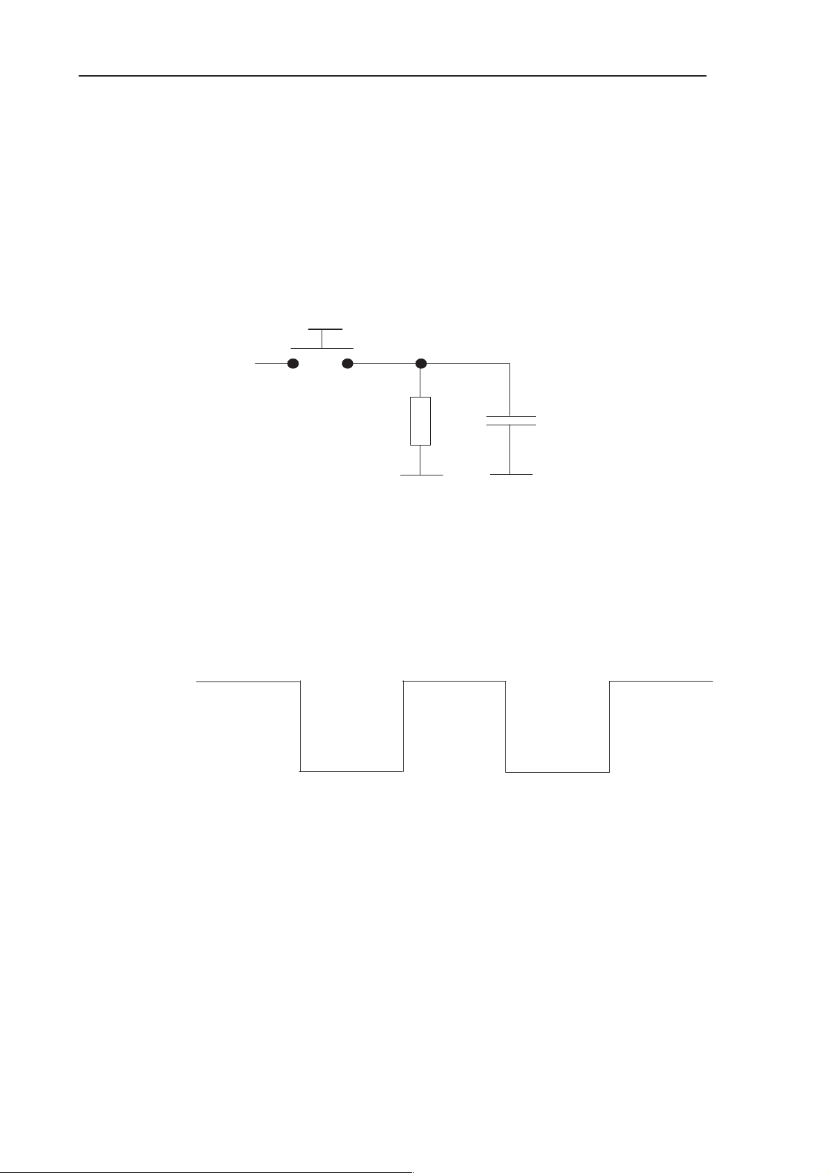
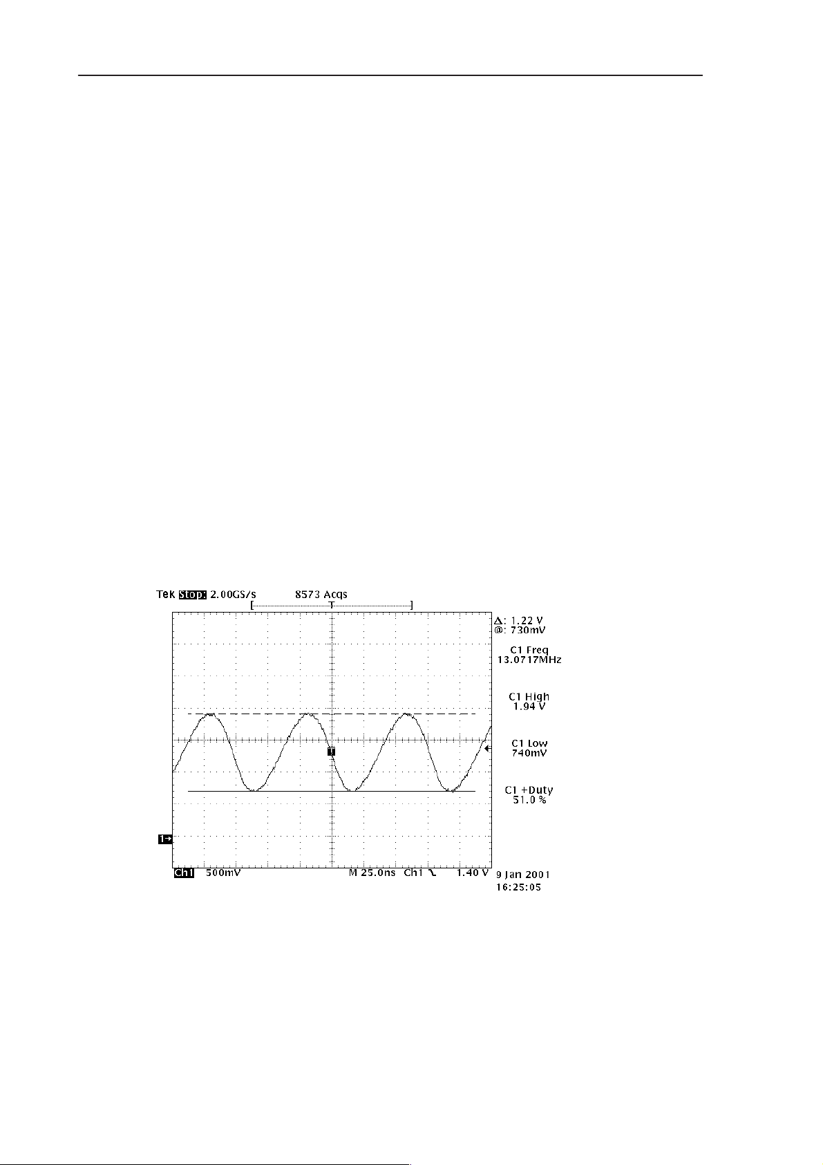
1 Measure RFC signal at C303. It should show 13.000 MHz sine wave,
approximately 1.2Vp–p with about 950mV DC–offset (see Figure 17). Check
the C303 capacitor.
• If this is OK, the processor gets the clock signal. The processor may
be faulty, or the fault is in the memories. Continue to ”Memories” section.
• If there is the clock signal, but there is no DC–offset (signal low level
around 0V), check the probe used so that it is not loading the signal. If the
probe is not responsible for missing DC–offset, try cycling the power a couple
of times. If this does not help, the clock slicer circuitry in the MADLinda (D300)
is faulty.
8. Troubleshooting
• If there is no clock signal at all, continue at 2.
Figure 17. Clock signal
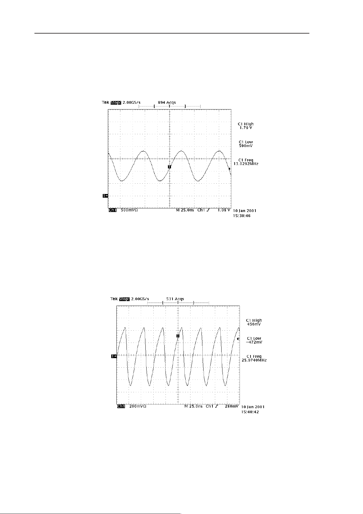
2. Check VXO power line at C553. It should be around 2.8V. If it is,
move to 4.
3. Check VCXOPwr (J302). It should be around 2.8V.
• If it is 2.8V, CCONT (N100) is faulty.
• If VCXOPwr is 0V, MADLinda (D300) has shut down the regulators
(sleep) or it is faulty. Cycle the power and re–check.
Issue 1 06/01
Page 8 – 27
Page 28
RAE-3
PAMS
8. Troubleshooting
1. Open the smaller RF shield metal can. Check Hagar RFC–out signal
at V800. It should show sine wave of 1.2V amplitude, 13MHz frequency (see
Figure 18 ).
• If this is OK, the problem is in V800 transistor or in R834, R830,
C834, L800.
Technical Documentation
Figure 18. 13 MHz sine wave
2. Check VTCXO output at R833. This should be 26MHz sine wave
(see Figure 19 ).
• If this is OK, Check R835, C830 for shorts and bad connections. If
they are OK, Hagar (N505) or C800 or R829 is faulty.
• If this is not OK,
check
VTCXO (G830).
R835, C830, R833 may be faulty. If they are OK,
Page 8 – 28
Figure 19. 26 MHz sine wave
Issue 1 06/01
Page 29

PAMS
RAE-3
Technical Documentation
2.8 Memory Tests
2.8.1 Test in boot up
FLASHes 0 (D351), 1 (D352) and 2 D(353):
– manufacturer and device id are read from each of the flashes then compared
to value stored in FLASH 0.
– id read program code is executed from API RAM
– If FLASH 0 is broken the phone will not boot up properly (user test code re-
sides in FLASH 0) i.e. probably not even blink CMT backlights.
– If one or more flash manufacturer and device id read fail CMT display back-
lights will blink 2 times in a loop.
SDRAM (D350):
– Data bus test:
• Test will detect if lines are stuck at high or low state
8. Troubleshooting
• Test will detect any bridging faults
– Address bus test:
• data is written to certain addresses and read back and verified
– tested lines: address bus, data bus, SDRRASX, SDRCASX, SDRWEX and
SDRCLK
– SDRDQMU, SDRDQML and SDRCKE functionality is tested only partly
– If either of these tests fail CMT display backlights will blink 3 times in a loop
Serial FLASH (D354):
– Id is read and id bits (3–5) are compared to value 0x30
– If the test fails CMT display backlights will blink 4 times in a loop
– tested lines: SEPI, SEPO and SEPClk
SEPCSX (low) and EXT_SYS_RESETX (high) tested partly
– problems found with test SW:
• id read fails and CMT backlights blink but serial flash is ok ⇒ problem is in MADLinda
Issue 1 06/01
Page 8 – 29
Page 30

RAE-3
PAMS
8. Troubleshooting
2.8.2 Test in PTS/WinTesla flashing
These tests are in the beginning of device flashing. If any of these tests fail the
flashing will be stopped and a notification will be shown on the monitor screen.
SDRAM (D350):
– data is written to certain addresses, read back and compared
FLASHes 0 (D351), 1 (D352) and 2 D(353):
– device and manufacturer ids are read from each of the flashes and then the
values are compared (same test as in boot up)
Serial FLASH (D354):
– device id is read and the value is compared (same test as in boot up)
Technical Documentation
Page 8 – 30
Issue 1 06/01
Page 31

PAMS
RAE-3
Technical Documentation
8. Troubleshooting
2.9 Memory Troubleshooting
2.9.1 Memory fails In Boot Up tests, CMT Backlight is blinking
If the device won’t boot up and CMT display backlight is blinking
⇒ FLASH 0 (D351) probably ok !
To measure signals from D352, D353, D350 and D354 the device needs to re-
booted up constantly since the lines are active only a short time in the beginning of the boot.
Also CCONT WATCHDOG will shut the device off after 32 seconds !
Time between each memory device blinks is 1 second and time between differ-
ent memory device blinks is 2 seconds.
For example if FLASH1 and Serial Flash are broken the blinking sequence
goes:
2 blinks with 1 sec interval (FLASH fault)
2 sec without blinks
4 blinks with 1 sec intervals (Serial Flash fault)
2 sec without blinks
then to the beginning again
Issue 1 06/01
Page 8 – 31
Page 32
RAE-3
PAMS
8. Troubleshooting
Technical Documentation
2.9.2 CMT display backlight blinking 2 times in a loop
CMT display backlight blinking 2 times in a loop (”Flash fault”):
Manufacturer and device id read from FLASH 1 (D352) or FLASH 2 (D353) or
from both fails.
ID read from FLASH1 or
FLASH2 fails
Flash the device
D352 ID read
fails during flashing
D353 ID read
fails during flashing
negative pulses
NO
Problem in
D300 (MCU)
See FLASH signal pictures later.
Check:
on J339
(1.8V)
OK?
YES
Change
D352
Figure 20.
YES
Change
D353
Check:
negative pulses
on J340
(1.8v)
OK?
NO
Problem in
D300 (MCU)
Page 8 – 32
Issue 1 06/01
Page 33

PAMS
RAE-3
Technical Documentation
8. Troubleshooting
2.9.3 CMT display backlight blinking 3 times in a loop
CMT display backlight blinking 3 times in a loop (”SDRAM fault”):
D350 SDRAM test fails
Check activity from SDRAM lilnes
SDRRASX (J312): negative pulses (2.8V) SDRCASX (J313): negative pulses (2.8V)
SDRWEX (J314): negative pulses(2.8V) SDRCLK (J310): 13MHz clock (2.8V)
SDRAd6 (J348): postive pulses (2.8V) SDRDQML (J315): negative pulses (2.8V)
SDRDQMU (J316): negative pulses (2.8V) SDRCKE (J311): high (2.8V)
SDRDa8 (J349): positive pulses (data pulses driven by SDRAM have bigger
over shoot spikes than data driven by MADLinda MCU, see figure 23) (2.8V)
Pulses on MADLinda control lines J312, J313, J314,
J310, J348, J315, J316 or J349
NO
Replace D350 if J349
D300 faulty
Figure 21.
data pulses with big
overshoot spikes are
missing
OK
Issue 1 06/01
Page 8 – 33
Page 34

RAE-3
PAMS
8. Troubleshooting
SDRDa8
J349
Technical Documentation
Figure 22. SDRAM (D350) driven data line SDRDa8 (J349)
SDRCLK
J310
SDRRASX
J312
SDRCASX
J313
SDRWEX
J314
Figure 23. SDRAM signals and levels 1
Page 8 – 34
Issue 1 06/01
Page 35

PAMS
RAE-3
Technical Documentation
SDRCLK
J310
SDRAd6
J348
SDRDQML
J315
SDRCKE
J311
8. Troubleshooting
Figure 24. SDRAM signals and levels 2
Issue 1 06/01
Page 8 – 35
Page 36

RAE-3
PAMS
8. Troubleshooting
Technical Documentation
2.9.4 CMT display backlight blinking 4 times in a loop
CMT display backlight blinking 4 times in a loop (”Serial Flash fault”):
D354 Serial Flash ID read
Check activity in serial FLASH lines
SEPClk (J327):6.5MHz clock (2.8V)
SEPO (J329): positive pulses (2.8V)
SEPCSX (J337): long negative pulse (2.8V)
EXT_SYS_RESETX (J301): high (2.8V)
SER_FL_RBY(J346): high (D300 internal pull–up, use passive
probe!) (2.8V)
SEPI (J328): Positive pulses
(D300 internal pull–up) (2.8V)
test fails
If no pulses found from J327, J328, J329 or from J337
problem is in D300
If J301 or J346 are low problem is D300
Figure 25.
If J328 stays always high change D354
Page 8 – 36
Issue 1 06/01
Page 37

PAMS
RAE-3
Technical Documentation
SEPCLK
J327
SEPO
J329
SEPI
J328
SEPCSX
J337
Figure 26. Serial Flash (D354) id read sequence.
8. Troubleshooting
Issue 1 06/01
Page 8 – 37
Page 38

RAE-3
PAMS
8. Troubleshooting
2.9.5 Memory fails in PTS/WinTesla flashing
1. SDRAM id read test fails
Refer to the previous ”SDRAM fault” chapter.
2. Flash manufacturer and device id read fails
a) If id read from all of the three flashes (D351, D352 and D353) fails
ly the problem is in D300.
Check D300 and control lines:
S FLDa7 (J351): positive pulses (1.8V)
S FLCS0X (J338): negative pulses (1.8V)
S FLOEX (J341): negative pulses (1.8V)
S FLCS1X (J339): negative pulses (1.8V)
S FLWEX (J342): negative pulses (1.8V)
S FLCS2X (J340): negative pulses (1.8V)
Technical Documentation
most like-
S FLAd5 (J350): positive pulses (1.8V)
S FLRPX (J343): high (1.8V)
S FLWPX (J347): low (1.8V)
If any of the signals is missing the problem is in D300.
b) If id read from one or two flashes fails
Page 8 – 38
Issue 1 06/01
Page 39
PAMS
RAE-3
Technical Documentation
D351 id read fails
D352 id read fails
Check if FLCS0X OK, J338
YES NO
NO
Check if FLCS1X OK, J339
8. Troubleshooting
ID read from FLASH fails
D353 id read fails
YES
Problem with
Change D352
D300
Check if FLCS2X OK, J340
NO
Change D353
Figure 27.
Refer to the oscilloscope screen shots next page for what the signals should
look like.
YES
Issue 1 06/01
Page 8 – 39
Page 40

RAE-3
PAMS
8. Troubleshooting
FLCS0X
J338
FLOEX
J341
FLWEX
J342
Figure 28. Flash 0 (D351) manufacturer and device id read
Technical Documentation
FLAd5
J350
FLDa7
J351
Figure 29. the Flash address and databus signals
2.9.6 Serial Flash id read test fails
Refer to previous chapter ”Serial Flash fault” 2.1.2
Page 8 – 40
Issue 1 06/01
Page 41
PAMS
RAE-3
Technical Documentation
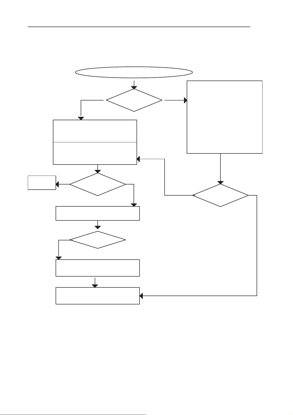
2.10 Serial Interface Troubleshooting
Serial Interface problem
YES NO
Activate WinTesla,
observe
ADC–readings
Check that ”DTR Detection”
state changes by pressing
ACC_VOLT AGE switch
in the service jig
Flashing
successful?
8. Troubleshooting
1. Check Serial connector
X450 spring contacts
2. Check and replace
ESD protection device V451
3. Check DCE_Tx (AccRxData)
comp. R452, C458, R300
4. Check DCE_Rx (AccTxData)
comp. R453, C457, R307
5. Check DCE_DCD (MBus)
comp. R450, C453, R309
NO
Serial I/O
OK
NO
YES NO
OK?
Check DCE_DTR line
comp. R454, C459,V489, R310
OK?
Refer to Accessory power
output troubleshooting
OK
Faulty MAD (N300)
or PWB fault
Figure 30.
NOTE1: Ensure that the customer’s DLR–2L is OK.
Flashing
successful?
YES
NOTE2: Wintesla ADC–readings for ’DTR Detection’: state ”0” = DCE_DTR
– line at 2.8 – 3.0V
– line at 0 – 0.3V
NOTE3: Signal levels in practice: High 2.7V, Low 0.3V
Exception: Diode in DTR line causes voltage drop, see Figure 31 below:
Issue 1 06/01
Wintesla ADC–readings for ’DTR Detection’: state ”1” = DCE_DTR
Page 8 – 41
Page 42

RAE-3
PAMS
8. Troubleshooting
0.3V
Technical Documentation
2.95V
2.8V
With DLR–2L
C1, black: MAD end
C5, green: syscon end
Using DLR–2:
GRP1, black: MAD end
GRP2: System connector end
0 V
Figure 31. DTH line voltage
Page 8 – 42
Issue 1 06/01
Page 43
PAMS
RAE-3
Technical Documentation
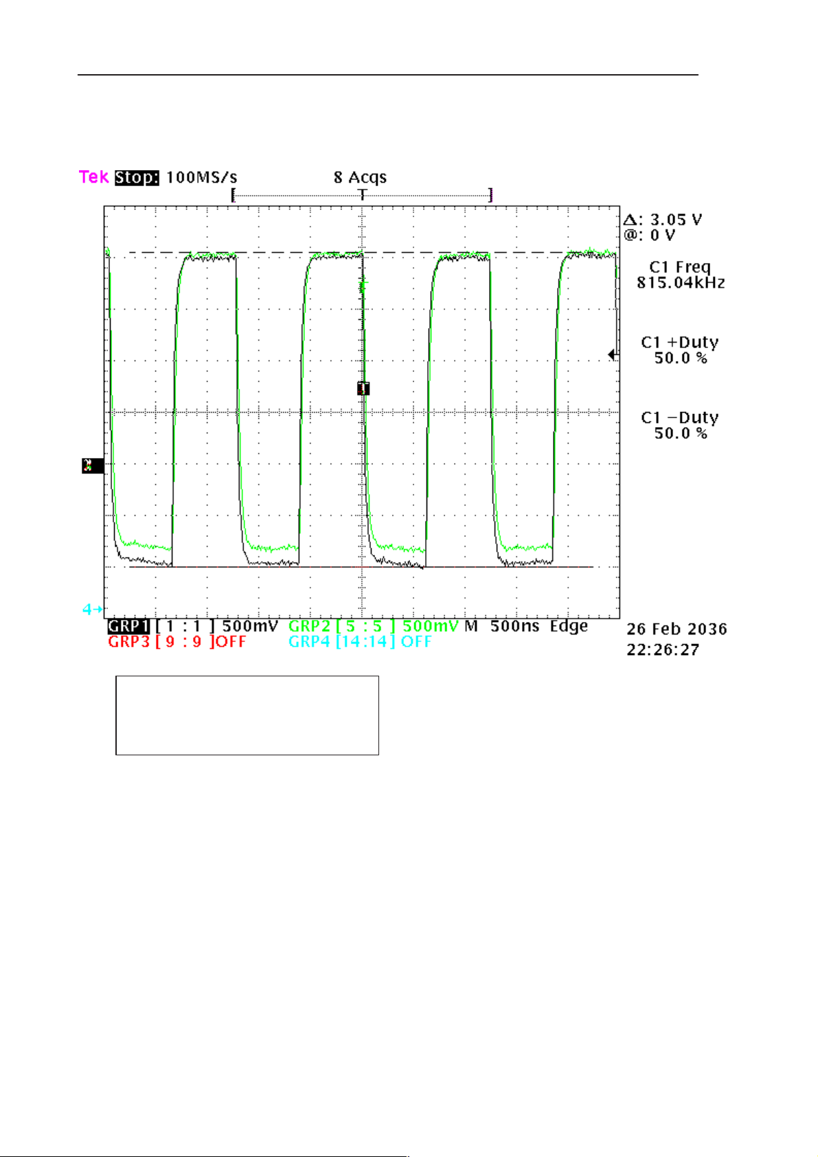
MBUS (clock) Signal during flashing (Figure 32):
8. Troubleshooting
GRP1, black: MAD–end
GRP2: system connector end
Approx. 0.2V difference results from MBUS
pull–up resistor (R309, 4k7) & serial resistor
(R450, 270R) voltage slicing.
Figure 32. MBUS (clock) Signal during flashing
Issue 1 06/01
Page 8 – 43
Page 44

RAE-3
PAMS
8. Troubleshooting
2.11 CONTACT SERVICE in CMT display
CONTACT SERVICE in CMT display (Self-tests with WinTesla)
Display Information: ”Contact Service”
This fault means that software is able to run and thus the watchdog of CCONT
(N100) can be served. Self–test functions are executed when power is switched
on and software is started to execute from flash.
If any one of the self–tests fails (except no. 3, 7, 8, and F), the text ”Contact
Service” is shown in the phone display.
MCU Self–tests are divided into those executed while power up (tests: 1–5 and
9–I ) and the ones can be executed with the connected PC. The tests and included items are as follows (Figure 33, screendump from the WinTesla)
Technical Documentation
The information can be used for diagnosis.
Memory tests differ from normal DCT3 self–tests. They can not be executed in
the ENOS because memory protection.
There is no EEPROM. The EEPROM is emulated in the FLASH (part of CS2).
All contents where EEPROM is mentioned refer to emulated EEPROM.
Item no. 1; MCU ROM Checksum:
Page 8 – 44
Figure 33.
Issue 1 06/01
Page 45

PAMS
RAE-3
Technical Documentation
Calculates 16 bit checksum out of Flash code and compares it to the one found
in Flash. Items being checked are MADLinda <–> Flash data– and address
lines FLDa0–15 and FLAd1–21, FLCS0X (CE0), FLCS1X (CE1), FLCS2X
(CE2), FLWEX (WE), Vbb (Vcc), VCORE (Vccq), GND, and Flash internal functionality.
Item no. 2 MCU EEPROM Interface:
Checks current PMM error status. If this test FAILs, the PMM data is not valid
anymore and should be formatted.
Item no. D COBBA Serial
This test tests Audio interface (PCM) of the COBBA_GJP.
Item no. E COBBA Parallel
This test tests the serial control/RF interface of the COBBA_GJP.
8. Troubleshooting
Issue 1 06/01
Page 8 – 45
Page 46

RAE-3
PAMS
8. Troubleshooting
Technical Documentation
2.12 CCONT Serial interface Troubleshooting
If there are problems in CCONT’s serial control interface, self tests fail and
there is ”Contact service” shown on the display. Wintesla shows this fail as
”CCONT Interface”.
NOTE: Low level means 0V, high level means approximately 2.8V.
Check GENSCLK line at J318
Square wave, Freq. 2.17 MHz ?
(see note below?)
Check CCONTCSX line at J317
Activity?
Signal active low
Check GENSDIO line at R308
Activity?
Signal active high
Check all three lines simultaneously , see fig. below
OK?
YES
NO
D300 or PWB
faulty
Figure 34.
(Note: Measurement should show 2.17MHz square wave. This interface is connected to CMT display also, so there is other activity too. The 3.1MHz clock is
targeted for CMT display, do not worry about that. The clock signal is low when
inactive.)
1. Measure all the three lines simultaneously (Figure 35).
Set the trigger to CCONTCSX line falling edge.
You should see the two cases, Figure 35 and Figure 36 .
(Channel 1–GENSClk,
Channel 2–CCONTCSX,
Channel 3–GENSDIO). High level is about 2.8V
Page 8 – 46
Figure 35.
Issue 1 06/01
Page 47

PAMS
RAE-3
Technical Documentation
MADLinda writes to CCONT. The data at sixth bit is ’0’ as marked with the cursors. The data after the read/write bit varies, just like the address before the bit.
If you can see this kind of traffic, MADLinda side of the interface is functioning
correctly.
8. Troubleshooting
Figure 36.
MADLinda reads from CCONT. The data at sixth bit is ’1’, marked with the cursors. There should be data seen after the ’read’ bit. All zero values may be
read, but there should be other data seen, too. CCONT read cycles are fairly
rare compared to write cycles. If there is not any non–zero reads from CCONT,
the CCONT (N100) may be faulty.
Issue 1 06/01
Page 8 – 47
Page 48
RAE-3
PAMS
8. Troubleshooting
2.13 SIM Card
2.13.1 SIM Card Error Troubleshooting
The fault information ”SIM Card error” means most likely that the SIM locked
phone has been inserted with a SIM which does not correspond to the lock
code.
Check the SIM lock status of the phone with WinTesla:
”SIM Card Error”
message in display ?
Set the phone in NORMAL mode
Technical Documentation
View–> Quick/RF Info
See ”SIM Lock Settings” field:
Blank
NO
SIM lock activated: inform customer
Customer contacts network operator
to ask for lock reset
field?
YES
Figure 37.
No SIM lock.
Refer to ”SIM Card Rejected”
troubleshooting
Page 8 – 48
Issue 1 06/01
Page 49

PAMS
RAE-3
Technical Documentation
2.13.2 SIM Card Rejected
The fault information ”SIM Card rejected” means that the ATR message (Answer To Reset; the first message from SIM card to phone after SIM card power
up) is sent, but it is corrupted somehow, eg. the dataline signal levels are wrong
or factory set values (stored in the EEPROM) are not correct.
NOTE1: CHECK THE MEASUREMENT POINT PICTURE BEFORE SERVICE
ACTIONS
SIM_xxx_Cardside – refers to signal which exists in SIM card contacts
SIM_xxx_o – refers to signal which exists in CCONT(N100) side
NOTE2: SIM Signals between CCONT (N100) and LindaMAD (D300) are not
possible to measure in bl8–module because traces are running in inner layers
of PWB.
8. Troubleshooting
Issue 1 06/01
Page 8 – 49
Page 50
RAE-3
PAMS
8. Troubleshooting
5V card:Check
5V charge pump
components
C107
V101
C110
Still
problem?
SIM CARD FAULT
Check VSIM at SIM card pin
NO
VSIM=
2,8V min. with 3V
4.5V min. with 5V
Check V103 pins
card
Pin_1: CLK
Pin_6: DA TA
Pin_4: Reset
YES
YES
card
Technical Documentation
NO
3V card: Check
N100 (CCONT)
C112, C113
Replace
if necessary
YES
Replace
N100
(CCONT)
D300 (MAD) faulty
Lines
rising
0V –>3V/5V
after power on
Check ATR data at
N100
R112
at N100 (CCCONT)
side /SIM_DA TA_0
Check
N100 (CCONT)
YES
problem?
?
OK?
Still
YES
YES
NO
NO
NO
Check
SIM card reader
mechanical
connections
and eventual
short circuits from
CLK, DA TA and
RESET lines
against GND
Check
X101, V103,
R109, R112
R125
N100 faulty
Page 8 – 50
Figure 38.
Issue 1 06/01
Page 51

PAMS
RAE-3
Technical Documentation
2.13.3 Insert SIM card
The hardware of the SIM interface from the MADLinda (D300) to the SIM connector (X101) can be tested without SIM card. This leaves SIM connector
(X101) contacts to be used as an measurement points.
When the power is switched on and if the BSI line (X100:2) is grounded by resistor (which happens automatically in service jig), all the used lines (VSIM,
RST, CLK & DATA) rise up to 3V and/or 5V four times (SW tries to ask SIM card
four times).
NOTE1: CHECK THE MEASUREMENT POINT PICTURE BEFORE SERVICE
ACTIONS
SIM_xxx_Cardside – refers to signal which exists in SIM card contacts
SIM_xxx_o – refers to signal which exists in CCONT(N100) side
NOTE2: SIM Signals between CCONT (N100) and LindaMAD (D300) are not
possible to measure in BL8–module because traces are running in inner layers
of PWB.
8. Troubleshooting
Issue 1 06/01
Page 8 – 51
Page 52

RAE-3
PAMS
8. Troubleshooting
5V card:Check
5V charge pump
components
C107
V101
C110
Still
problem?
Insert SIM card fault
YES
Check Voltage level between R121 and C126
When BSI resistor connected (included in
service jig
YES
NO
Volt.level
<1.5V ?
YES
NO–5V
Check VSIM, DA TA, RESET, CLOCK lines
at the pins of ASIM connector (X100)
VSIM at SIM card pin
2.8V min. with 3V card
4.5V with 5V card
YES
or SIM_xxx cardside signals at
measurement points
Technical Documentation
Check
R121, R122,
X100, C126
3V card: Check
NO– 3V
N100 (CCONT)
C112, C113
Replace
if necessary
YES
Faulty
N100
(CCONT)
Faulty PWB
Faulty D300
Still
problem?
Replace D300 (MAD)
YES
Lines
rising 0V–>3V/5V
after power on ?
NO
Check VSIM (V103 pin 3)
DATA_0 (R109)
SIMRST_0 (R125) at
(ref. Measurement point diagram)
N100/CCONT side
NO
rising 0V–>3V/5V
after power on ?
N100 (CCONT)
NO
Lines
Replace
Still
problem?
NO
YES
YES
YES
Check SIM card,
SIM card reader
mechanical
connections
Check
X100, V103
R109, R112
R125
SIM I/O OK,
N100 (CCONT)
faulty
Page 8 – 52
Figure 39.
Issue 1 06/01
Page 53

PAMS
RAE-3
Technical Documentation
2.14 Memory Card
2.14.1 Memory Card Interface Troubleshooting
Start with assembled device with a faultless memory card inserted.
If necessary, proceed with tests in the jig with the faultless memory card in-
serted.
Clk, Cmd and Data OK means that frequency, rise and fall timing are OK during
various operating modes.
Note:
During initialization phase (MMCClk = lower frequency) the response via
MMCCmd line from card to MAD is sent in open drain mode i.e. rise time is
about 1us.
Voltage of MMCCmd and MMCDa signals depends on direction of transfer
(MAD I/O voltage is 2.8V and Card I/O is 3.0V).
Test pads J10x are located on the JL4 board of the Module Jig.
8. Troubleshooting
Troubleshooting diagram next page, Figure 40.
Issue 1 06/01
Page 8 – 53
Page 54

RAE-3
PAMS
8. Troubleshooting
Memory card
interface check
Run WinTesla
Memory card
test
Test
OK?
NO
Run Memory Card
cover Switch
fault test
Switch
OK ?
NO
Ref
Memory card
cover switch
fault tree
YES
YES
Technical Documentation
A faulty Memory Card used before ?
SW corruption ?
Assembled device
Disassembled device in jig
Measure VMMC
J104 while re–running
the MemCard test
NO
2.9 – 3.1V ?
YES
Measure MMCClk
J105 while re–running
the test
NO
Clk OK ?
YES
Measure MMCCmd
J102 while
re–running the test
Check X001/4
Measure N103/1
(control from
MAD while
re–running the
test
Check X001/5
R004 and
V001/4
Parts OK?
MAD I/O
fault
NO
Ctrl
OK?
YES
Check
N103
C114
C123
C124
R007
C001
YES
Page 8 – 54
CMD OK ?
YES
Measure MMCDa J107
Data OK?
YES
Figure 40.
NO
NO
Check X001/2
R005, R002
V001/3
OK?
Check X001/7
R001, R003
and V001/6
Parts OK ?
Issue 1 06/01
YES
YES
MAD I/OUndefined CPU error
fault
Page 55
PAMS
RAE-3
Technical Documentation
2.14.2 Memory card switch troubleshooting:
NOTE1: Memory card switch pressed (lid closed) => ADC reading ’Memory
Card Cover Detection’ is in state ”0” => MMC_Switch – line = 0V
Memory card switch released (lid opened) => ADC reading ’Memory Card Cover Detection’ is in state ”1” => MMC_Switch – line = 2.8V
MMC Card cover switch
Open RAE3 lid after boot
problem
YES
Open WinTesla
Testing–>
ADC Readings
OK
MMC
lid open
according to
WinTesla ?
*
8. Troubleshooting
YESNO
Close MMC card cover and
wait updated values
from WinTesla
Check J001
(MMC switch)
OK
Check C002 and V001
OK?
Faulty
circuit
D300 (MAD)
or PWB
Check
R006
OK?
* note:
Cover opened MMC cover detection =”1”
Cover closed MMC cover detection = ”0”
Check mech.
functionality
of J001
check contact
surfaces
OK?
R006
faulty
NO
NO
MMC cover
switch J001
broken
Lid
closed
according to
WinTesla ?
MMC cover
switch J001
Figure 41.
*
YES
OK
Issue 1 06/01
Page 8 – 55
Page 56

RAE-3
PAMS
8. Troubleshooting
2.15 Lid Switch
2.15.1 Lid Switch Troubleshooting
NOTE1:
Lid signal (MAD pin P2 gendet) :
Lid closed = ’Cover Detection’ from Wintesla ADC readings is state ”0”
=> V301 (HALL) output = 2.8V
Lid opened = ’Cover Detection’ from Wintesla ADC readings is state ”1”
=> V301 (HALL) output = 0V
Troubleshooting diagram Figure 42 next page.
Technical Documentation
Page 8 – 56
Issue 1 06/01
Page 57

PAMS
RAE-3
Technical Documentation
Lid
switch
trouble–
shooting
ASSEMBLED DEVICE
DEVICE IN JIG
Check
V301, C322
NO
YES
Open Wintesla
Select Testing –>ADC Readings
Turn the phone power on
Open the lid
Wintesla:
Lid Open OK
(cover
detection
state
1) ?
NO
N301
pin 1
(Hall supply volt)
2.8V ?
8. Troubleshooting
Place magnet above the TAB key,
note: pole toward the key !
then
wait Refresh from Wintesla
Wintesla:
Lid Closed OK
(ADC reading
Cover
switch=
”0”
NO
YES
Lid switch
OK?
Check/replace
magnet
in the lid
Check
V301,
(solders) R302
If OK,
replace V301
Faulty PWB
Faulty
circuit
D300
(MAD)
or
NO
YES
Use serv.jig
magnet
Out–
put toggle
of V301 pin 3
low state
(<0.3V)
?
level at V301 pin 1
Out–
put toggle
of V301 pin 3
high
?
YES
Check
Hall supply volt.
(VBB) 2.8V
OK?
YES
Use serv.jig
magnet
NOYES
high voltage level
NO
Check
V301 solders
Short
circuit inC323 ?
R302:
(2.8V) at both
ends?
Check
V301, C322
Issue 1 06/01
Replace V301
Figure 42.
OK
NO
Check trace between
V301 pin3 and R302
Page 8 – 57
Page 58

RAE-3
PAMS
8. Troubleshooting
Technical Documentation
2.16 Battery Removal Switch troubleshooting
NOTE1: Switch itself is not possible to test in service jig.
NOTE2: Switch FREE position = Wintesla ADC–readings ’Battery Removal
Switch’ is in state ”0” =>BATT_REM – line = 2.8V
Switch CONNECTED position = Wintesla ADC–readings ’Battery Removal
Switch’ is in state ”1” => BATT_REM – line = 0V
NOTE3: Battery removal switch (latch spring) gets connected when battery
latch is pressed during battery release.
Refer to the diagram Figure 43 next page.
Page 8 – 58
Issue 1 06/01
Page 59
PAMS
RAE-3
Technical Documentation
Short circuit in
switch lines
(BATT_REM)
Check Z401
Reading
”1” though
YES NO
latch position
”FREE” ?
Battery removal switch
problem
YES
Open WinTesla
Testing–>
PDC readings
OK
Latch ”FREE” position
Battery
removal switch
state =”0”
?
8. Troubleshooting
YESNO
Keep latch in opposite position
wait updated values
from WinTesla
NO
State
changes to
”1” ?
YES
Faulty
circuit
D300
(MAD)
YES
Check B–to–B adapter
JC4 pin 42: BATT_REM
line:
Voltage
high (=2.8V)
?
Figure 43.
Battery removal
switch
OK
NO
1. Check latch spring and AF8 pads
2. Check B–to–B connector X400 of
UL8 and flex FL1
3. Check filter Z401 BATT_REM line
Issue 1 06/01
Page 8 – 59
Page 60

RAE-3
PAMS
8. Troubleshooting
Technical Documentation
2.17 COBBA Control Interface troubleshooting
NOTE: If there are problems in COBBA serial interface, self tests fail and there
is ”Contact service” shown on the display. Wintesla shows fails at ”Cobba parallel”.
Check COBBACLK line at J322
Square wave, Freq. 13MHz ?
Signal rising/falling edge 3 to 5 ns?
Signal duty cycle about 50per cent?
Low when inactive?
Check COBBASDA line at J324
Activity?
Signal rising/falling edge 3 to 5 ns?
High when inactive ?
OK?
YES
NO
D300 or PWB
faulty
Check COBBACSX line at J323
Activity?
Signal rising/falling edge 3 to 5 ns?
High when inactive ?
Check COBBARSTX a J321
High (about 2.8V) ?
Check all lines simultaneously , see fig. below
Figure 44.
Figure 45 is a write sequence to COBBA. There should be non–all–zero writes
to COBBA.
Page 8 – 60
Figure 45. Write sequence to COBBA.
Issue 1 06/01
Page 61

PAMS
RAE-3
Technical Documentation
Figure 46 is a COBBA read.
8. Troubleshooting
Figure 46. COBBA read
The MADLinda writes first the address to be read, deactivates the COBBACSX
line and then activates the COBBACSX line again. Then the COBBA_GJP
sends the requested data. There should be non–zero reads.
If no non–zero reads from COBBA can be seen, COBBA (N200) may be faulty.
If both reads and writes of non–zero values can be seen and the signal charac-
teristics were good, the COBBA serial control interface is working correctly.
Issue 1 06/01
Page 8 – 61
Page 62
RAE-3
PAMS
8. Troubleshooting
2.18 COBBA PCM Interface Troubleshooting
PCM interface transfers digital audio data. Problems in this interface result in
missing or flawed audio in either or both in uplink and downlink directions. If
Wintesla shows errors in ”COBBA serial interface”, PCM interface is faulty.
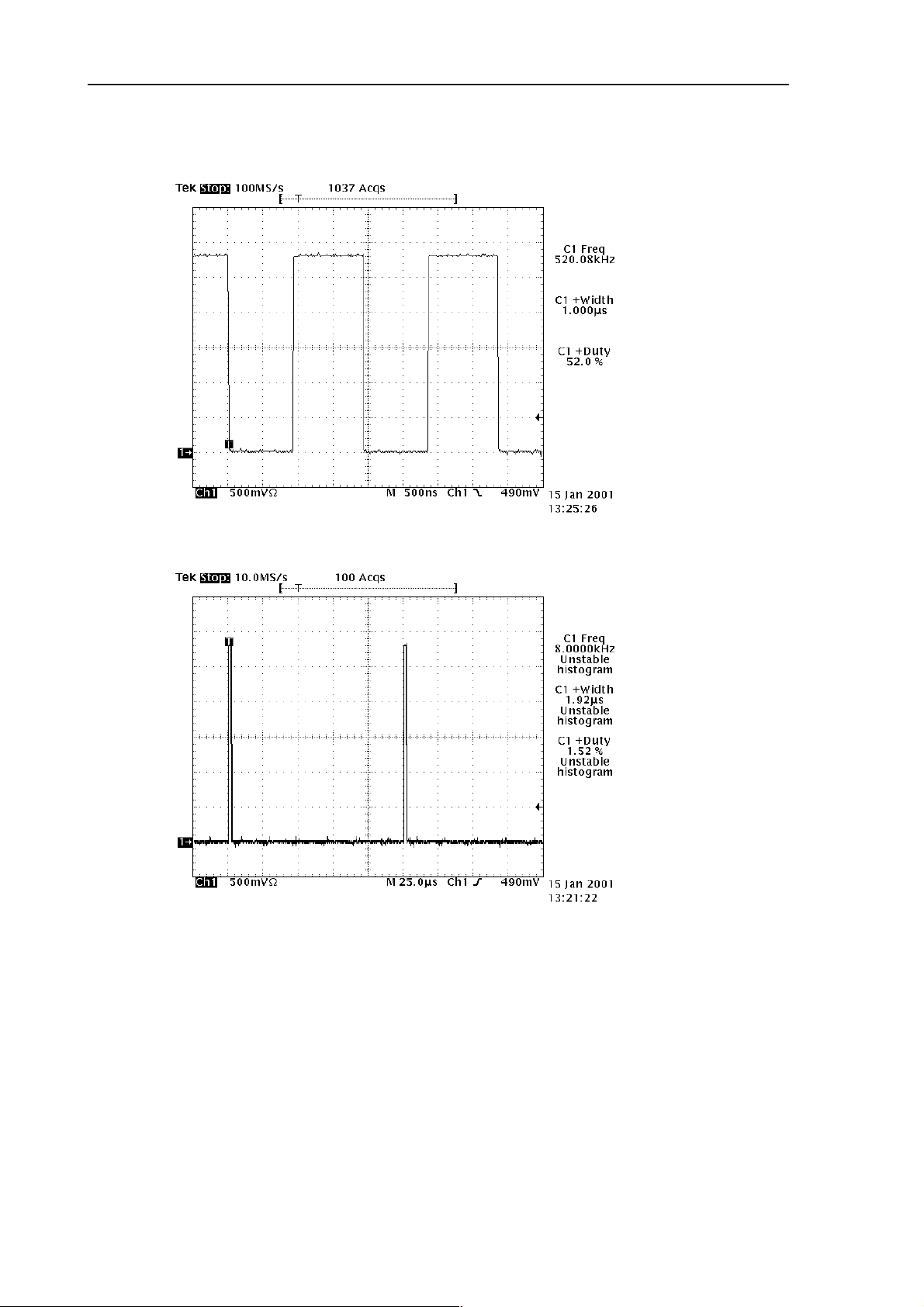
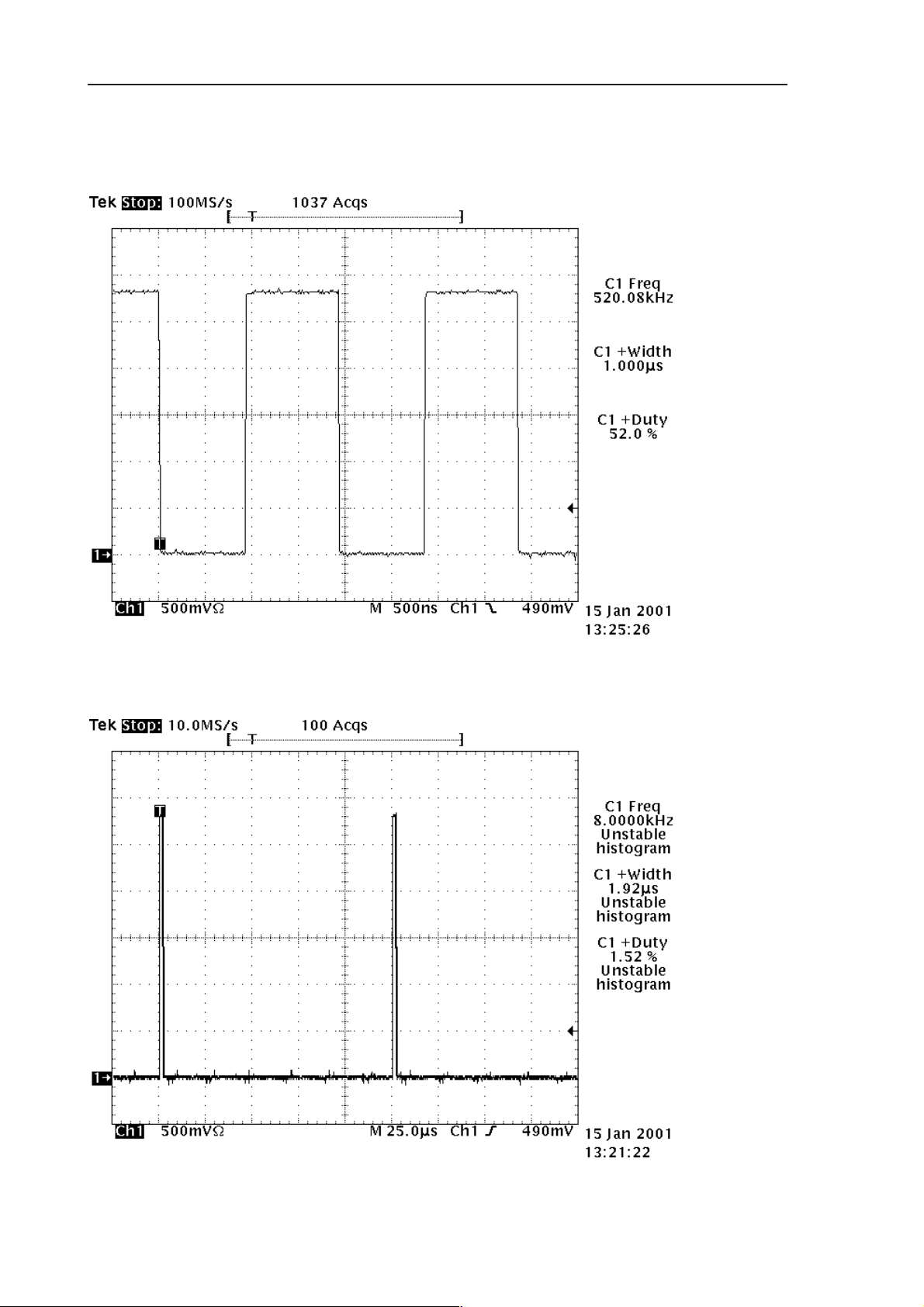
Check PCMDClk signal at J309:
520 kHz square wave
50 per cent duty cycle
Rising and falling edges about 3 to 5 ns
Inactive state low?
OK?
Check PCMSClk at J306
short pulse, rate 8.000kHz
1.52 per cent duty cycle
Rise and fall times about 3 to 5 ns
Inactive state low?
Ref. fig. 48
NOYES
N200 faulty
Ref. fig. 49
Technical Documentation
NOYES
OK?
Check PCMRx Data signal at J308
Activity during call and voice recording
If mic picks up sound, higher states at the cycle start
Rise and fall times about 3 to 5 ns
Signal idle state High with some 13MHz noise?
N200 faulty
Ref. fig. 50
NOYES
OK?
Check PCMTx data signal at J307
Activity during call
Rise and fall times about 4 to 7 ns
Idle statle low?
Ref. fig. 51
N200 faulty
There is no traffic in PCM interface without a call or audio play (voice recorder,
video player, etc). These signals can be measured with a call, which generates
Page 8 – 62
OK?
NO
N200 faulty
Figure 47.
Issue 1 06/01
Page 63
PAMS
RAE-3
Technical Documentation
traffic in both directions. Audio play generates traffic in one direction only. Recording audio (voice recorder) generates traffic in the other direction.
8. Troubleshooting
Figure 48. PCMDClk signal at J309
Figure 49. PCMSClk signal at J306.
Issue 1 06/01
Page 8 – 63
Page 64
RAE-3
PAMS
8. Troubleshooting
Technical Documentation
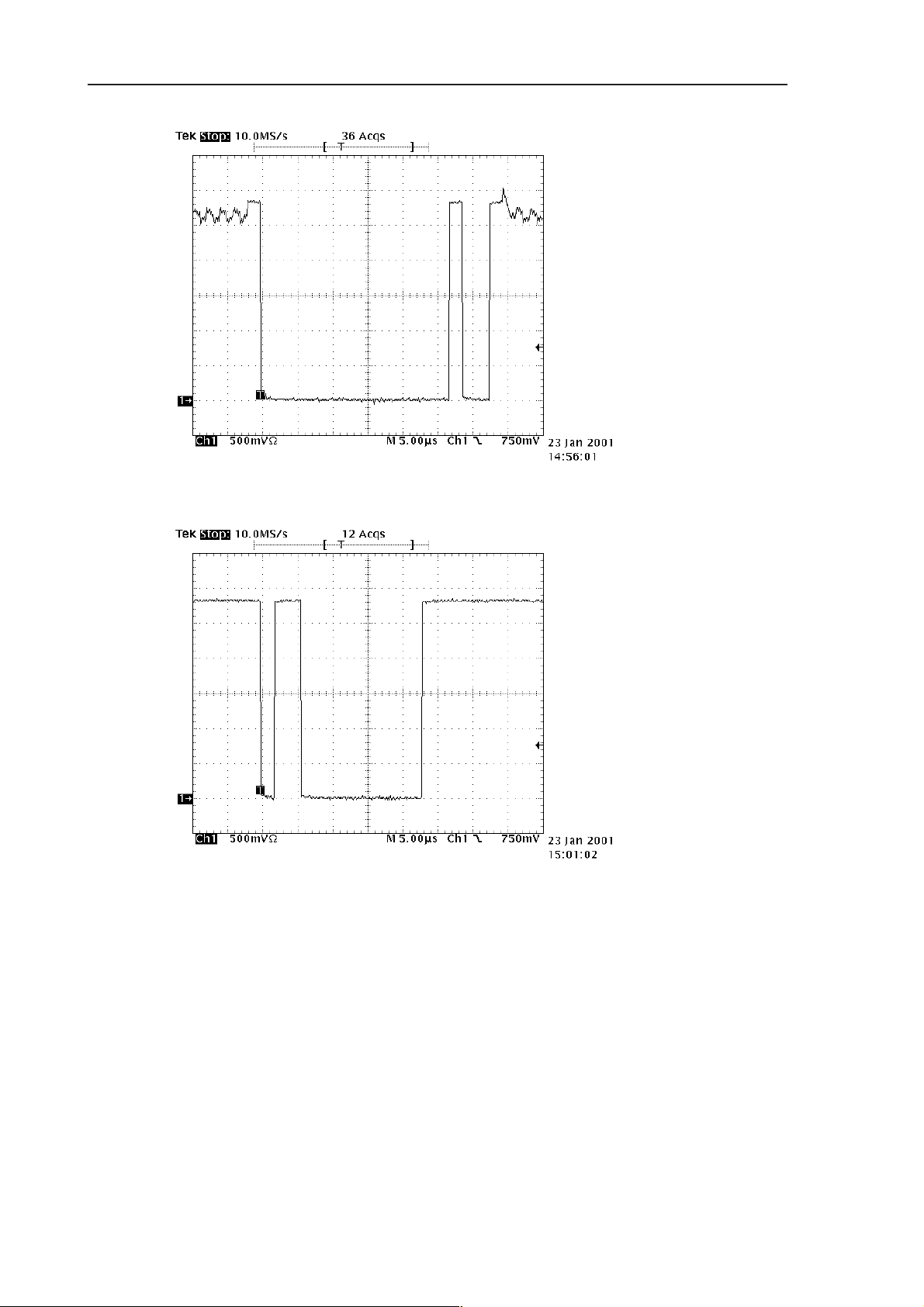
Figure 50. PCMRxData signal at J308.
PCMTxData signal at J307 (Figure 51). This signal comes from the other end’s
microphone or audio playing software (voice recorder, video player etc) and is
targeted for the earpiece or hands free speaker. There should be activity during
a call. Signal rise and fall times are around 4–7ns. Idle state is low.
Page 8 – 64
Figure 51. PCMTxData signal at J307
Issue 1 06/01
Page 65

PAMS
RAE-3
Technical Documentation
2.19 Audio troubleshooting
2.19.1 Both Mic and Earpiece/PHF faulty
MIC and Earpiece /PHF
faulty
Check voltage at cap C208
HOOKDET
without external audio devices
OK
HOOKDET
2,8V?
Check voltage at cap C202
HEADDET
without external audio devices
8. Troubleshooting
NO
Check
R206 and R207,
C208
* refer to section 2.17
in this document
OK
Check frequency at J309
PCMDClk during a call
OK
Check frequency at J306
PCMSClk during a call
HEADDET
2,8V?
520kHz
square wave 2.8Vpp
(ref.fig.53)
8 kHz
square wave 2.8Vpp
(ref.fig.54)
NO
Check
R203, R202, R200
C201,
C202
NO
Faulty
N200 (COBBA) *
NO
Faulty
N200 (COBBA) *
Issue 1 06/01
Figure 52. PCMDClk
Page 8 – 65
Page 66
RAE-3
PAMS
8. Troubleshooting
Technical Documentation
Figure 53. PCDClk
Page 8 – 66
Figure 54. PCMSClk
Issue 1 06/01
Page 67
PAMS
RAE-3
Technical Documentation
2.19.2 Mic faulty
MIC
faulty
Check microphone and mic connections to PWB
Check digital PCM data atJ308 (PCMRxData)
during a call
OK
Check voltages :
V202 pin 1 : 1.8V
V202 pin 3: 0.17V
OK
Data
OK?
during a call
Voltages
OK?
NO
NO
8. Troubleshooting
Faulty N200 (COBBA)
Refer to
COBBA control
interface troubleshooting
Check R222, R218
C231, C224,
C230
OK
DC voltage at C234 and C235
1.4V during call ?
OK
Check analog audio signal at
Voltages OK?
C232 during a call
Signal a few mV ?
*
NO
*
NO
Figure 55.
Mbias at R222
2.1V during call?
NO
Check
Check
C234, C235
C234, C235
C225, C240, R219,
R220 and PWB traces
OK
Check
*
Fault in
N200 (COBBA)
Note:* can not be measured in the service jig, because components are under
the SIM connector.
Use wire to measure them. After removing measurement wire, check that components are not defected. It is recommended to replace the components.
Issue 1 06/01
Page 8 – 67
Page 68

RAE-3
PAMS
8. Troubleshooting
2.19.3 Earpiece faulty
Earpiece
faulty
Check assembly of
earpiece and gasket
Check connections from
audio PWB to C229 and C228
OK
Check digital PCM data
at J307 (PCMTxData)
OK
Connection
during a call
OK?
Technical Documentation
1)
NO
Check Flex UL8 and
B–to–B conn X400
pins 47, 48
NO
Data
OK?
DC voltage at C228, C229
1.4V during call ?
OK
Check analog audio signal at
C228, C229 during a call
Voltages OK?
Signal a few mV ?
NO
NO
Faulty
D300 (MAD) 2)
Check R215, R216 and
connections.
Check
C228, C229
OK?
Faulty
N200 (COBBA)
Note:
1) If sound is distorted or too quiet fault is most probably in the gasket or in the
earpiece diaphragm.
2) Refer to section 2.16 in this document.
Page 8 – 68
Figure 56.
Issue 1 06/01
Page 69

PAMS
RAE-3
Technical Documentation
2.19.4 PHF Speaker faulty
Check assembly of HF speaker,
springs and connection to flex UL8
speaker pads to C236 and C237
OK
R201, R204, R205, R221
PHF Spealer
faulty
Check connections from
Connection
OK?
Check V AMP at
*
NO
8. Troubleshooting
Check Flex UL8 and
B–to–B conn X400
pins 43 to 46
Faulty
V200
OK
VAMP
about VBA TT ?
AMP SHDN at V200 pin 2
2.8 V during a PHF call ?
OK
Voltages OK?
Amplifier enabled?
Check voltage at N201 pin 1
NO
Voltage low?
NO
NO
OK
Check R201, R204, R205,
R221
C203, C204, C205, C206
*
Faulty
D300 (MAD)
(Note: R201, R221 only in BL8_18)
*
Note:
R204 and R205 havedifferent resistance
values in BL8_17
and BL8_18
Issue 1 06/01
Continues next page
Figure 57.
Page 8 – 69
Page 70
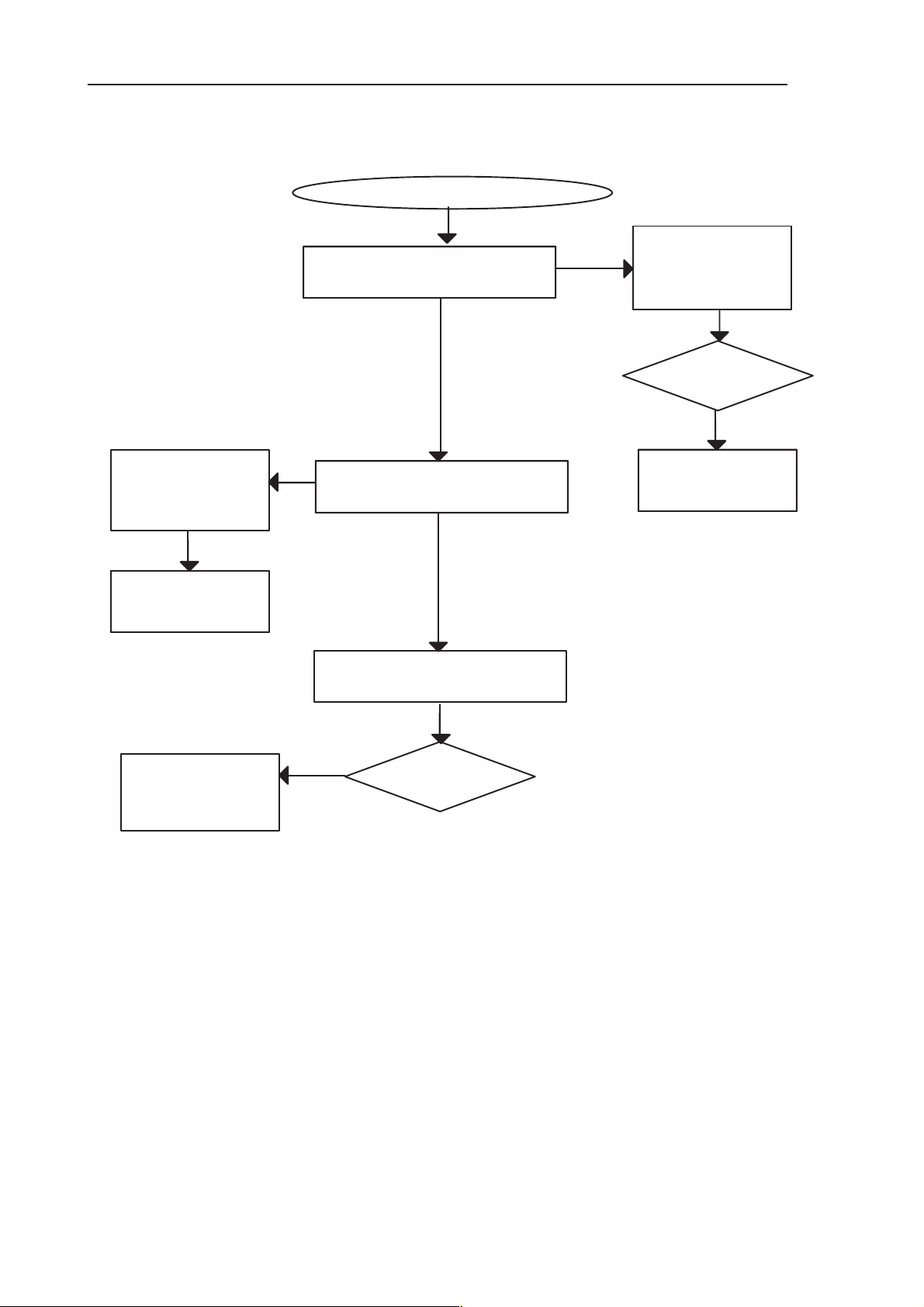
RAE-3
PAMS
8. Troubleshooting
Check R212, R213,
C220, C241, C223,
C217, C218
PHF speaker fault continued
Check analog audio input signal
XEAR at C220, min. some 10 mV
OK
NO
NO
Signal amplified (ca. 10x)
at N201 pins 5 and 8 ?
Technical Documentation
Check
NO
NO
R208, C213 and
XEAR traces from
C220 to N200
OK?
Faulty
Faulty
N200 (COBBA)
N200 (COBBA)
OK
Faulty
Faulty
N201 (audio amp)
Check
L200, L201,
PWB connections
OK
Analog audio signal at
C236 and C237?
NO
OK?
Figure 58.
Page 8 – 70
Issue 1 06/01
Page 71

PAMS
RAE-3
Technical Documentation
2.19.5 Headset out of order
Headset out of order
RAE–3
detects HS ?
OK
OK
(CMT lcd reads
”headset”)
Head–
set earpiece capsule
OK ?
NO
OK
D300 (MAD)
faulty
NO
8. Troubleshooting
Measurements
in Service Jig
Voltage
at C202 (HEADDET)
low ?
NO
Check XMIC and
SGND lines
from System Conn.
X450 pins 6 and 4
Check
C202, R203, L452
C464. R460, L450,
C462, R455, C460
C461, C452, C450
Head–
set Mic OK during
a call ?
Continues next page
voltage between
R200 and R202 is
1.5V during
OK
Check XEAR and GND lines
from System Conn
X450 pins 5 and 11
to COBBA and
R208, C213, L451,
C451, C463, R459
OK?
Check XMIC line from
System Conn X450 to N200
and
C207, C216, C215, C219
AUXOUT
NO
call?
Check C201
OK
N200 (COBBA) faulty
OK
Check N100
(CCONT) EAD value
with WinTesla
Accessor _
detection
NO
N100 or
D300 (MAD)
faulty
Issue 1 06/01
Figure 59.
Page 8 – 71
Page 72

RAE-3
PAMS
8. Troubleshooting
Headset out of order, continues
Remote control
OK
switch
OK ?
Head–
set faulty
NO
Check voltage at C208 while
HS switch button is pushed
OK
D300 (MAD)
faulty
Technical Documentation
Voltage
at C208 (HOOKDET)
low ?
Measurements
in Service Jig
NO
Check
R207 and C208
Figure 60.
Page 8 – 72
Issue 1 06/01
Page 73

PAMS
RAE-3
Technical Documentation
8. Troubleshooting
2.20 RF Interface
2.20.1 Phone doesn’t register to the network or doesn’t make a call
Phone does not register to the
network or does not
make a call
NO
NO
OK
NO
NO
Check C100, R211
Check CCONT N100
Check D300 MADLinda
Check D300 MADLinda
Check
Reser at
N600 pin1 =”1”
?
YES
Check
N600
C783
C784
C785
N505
(Hagar)
NO
Check supply voltage during RX slot:
YES
Check
R800
C793
D300
(MADLinda)
C101 (VCP) >4.8V
C133 (VRX) >2.7V
C135 (VSYN_1)>2.7V
C134 (VSYN_2)>2.7V
During TX slot:
C136 (VTX) >2.7V
Check synthesizer lines during RX slot:
C254 (VCOBBA)>2.7V ? Check N100 CCONT
YES
C100 (Vref) = 1.5V ?
YES
NO
SynthPwr (J319) = 1 (2.8V) ?
VCXO_Pwr (J302) = 1 (2.8V) ?
YES
N600 (VCHP) = 4.7V ?
YES
J502, J501/J505 SENA1
J501 (SCLK)
J500 (SDATA)
= Pulses ”0” –> ”1” ?
R800 (Reset) = ”1” ?
And
YES
Check RF part
YES
Check RF control lines during RX slot:
R708 (RxC, N240)= 0 – 2.3VB max.
R832 (AFC, VCXO)=0 – 1.2V typ.
YES
Check analog data signals during RX slot
R533 (RxIN, Cobba)=0 – 1.5V DC
C532 (RxIP, Cobba)=0 – 1.5V DC
Received signal is biased to DC,
nominal amplitude=
50mVpp, freq.=13MHz
YES
Check RF control lines during TX slot:
R792 (TxC, Cobba)=0 – 2.3V max.
J320(TxP) = ”0” –> ”1”(2.8V)
YES
Check analog data signals during TX slot:
R541 (TxIN, Cobba)
R541 (TxIP, Cobba)
R546 (TxQN, Cobba)
R546 (TxQP, Cobba)
Transmitted signal is biased to DC,
nom.ampl=300mVpp, freq.=64kHz
Figure 61.
NO
NO
NO
Check N200 COBBA
If DC failure:
Check N200 Cobba,
Check RF part
If TxC failure:
Check N200 Cobba,
If TxP failure,
Check D300
NO
Check N200 COBBA
else
R541, R546,
C540, C541
Issue 1 06/01
Page 8 – 73
Page 74
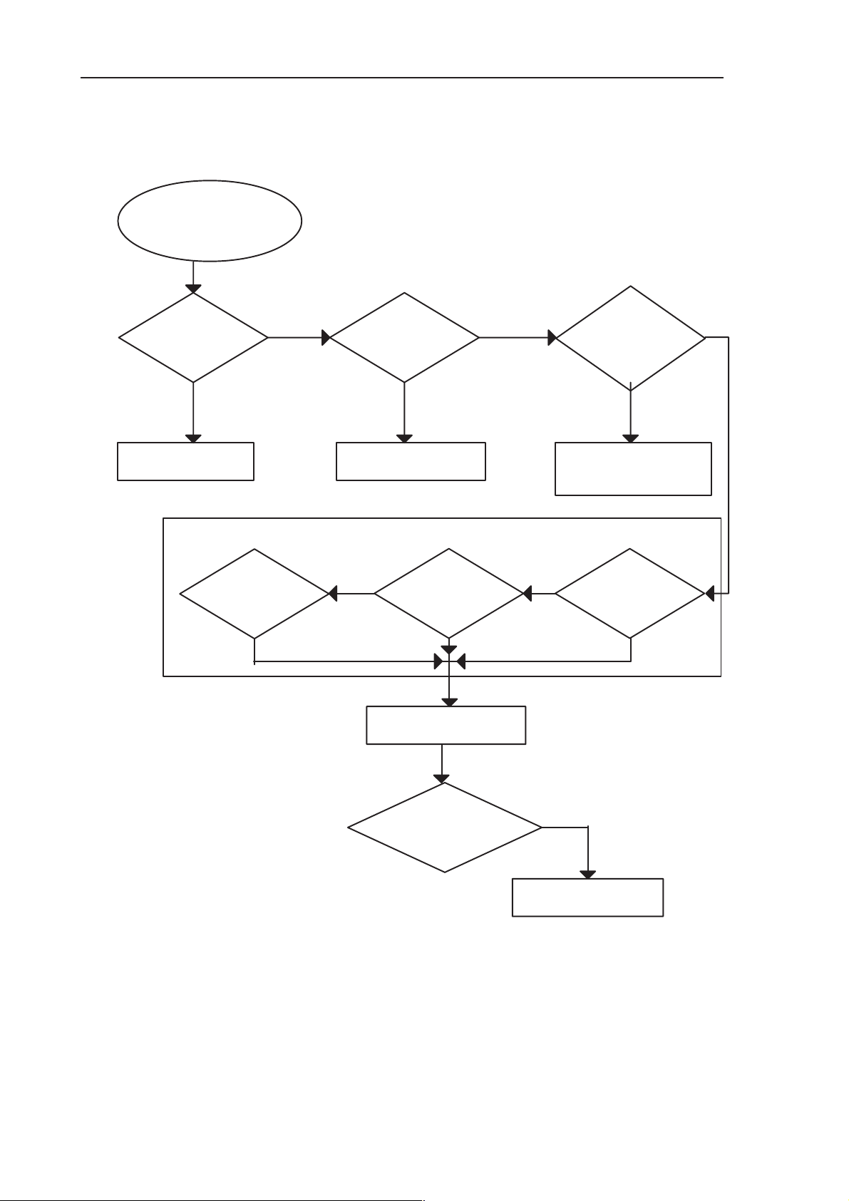
RAE-3
PAMS
8. Troubleshooting
2.21 IR Interface Troubleshooting diagram
IR CHECK
IR test OK?
(Wintesla)
YES NO
IrDA test OK
VBB (Vcc)
OK?
(N050/6)
NO
C052 – C054 OK?
Technical Documentation
YES
IRED_A(Vled)
(N050/1)
OK?
R050, R052, R053,
R054, C055, C050
OK?
CANNOT BE MEASURED IN THE JIG
YES YES
IREN (Sd)
OK?
(N050/5)
NO NO NO
IRDI (Rxd)
OK ?
(N050/4)
Replace IR module
IR Test
OK?
(Wintesla)
NO
IRDO (Txd)
(N050/3)
CPU fault
OK ?
Page 8 – 74
Figure 62.
Issue 1 06/01
Page 75

PAMS
RAE-3
Technical Documentation
2.22 BL8 related Keyboard problems
There may be several types of problems with keyboard. Usually some of the
keys (CMT and PDA) are not working, or several key presses happen simultaneously.
If CMT informs ”Please close cover”, see ”Lid switch problems” section.
8. Troubleshooting
Issue 1 06/01
Page 8 – 75
Page 76

RAE-3
PAMS
8. Troubleshooting
Put BL8 module in test jig, connect B–to–B adapter JC4.
DO NOT connect the UI module or Flex, yet
DO NOT switch power on.
Refer to table 6.
Problem with QWERTY
keypad _1
Check the resistance of Row and Col signals to GND.1)
Resistance > 1 MOhm ?
OK?
Turn power on.
DO NOT connect the UI module or Flex yet.
Check Col signals at pins:
49, 62, 60, 59, 54, 55, 56, 61, 53, 51
Voltage around 2.8V ?
NOYES
Check, replace
Z401 to Z404
Technical Documentation
YES
NO
OK?
Check Row signals at pins:
50, 69, 67, 65, 64, 63, 57, 68, 58, 52
Voltage around 0 V ?
YES
NO
OK?
Continue at next diagram
Figure 63.
Check, replace
CSP filters Z401 to Z404
if voltage = 0
Check, replace
CSP filters Z401 to Z404
Eliminate short circuits if
if voltage >0
Note 1) Pins 49–65 and
66–69 against pin 70 (gnd).
Page 8 – 76
Issue 1 06/01
Page 77
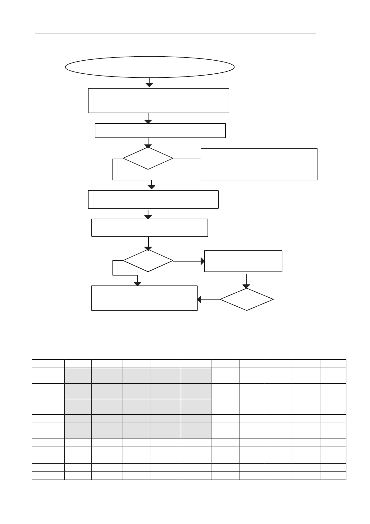
PAMS
RAE-3
Technical Documentation
Connect ROW0 to COL0
Measure the short circuit with oscilloscope
Signal rise and fall times between 80 to 120 ns,
constant activity?
Repeat for each ROW– COL pair.
Connect Flex and UI module to the jig.
Switch the power on, wait for reboot
Problem with QWERTY
keypad _2
OK?
8. Troubleshooting
NOYES
Cycle the power, retry
If no activity or rise/fall times our of range
check
CSP filters Z401 to Z404
Push the faulty key, check the column signal.
Signal rise/fall time 120 to 200 ns? (1)
Check, replace
CSP filters Z401 to Z404
YES
OK?
YES
OK?
D300 faulty
NO
Figure 64.
Table 1. Keyboard matrix (keys on UL2 module highlighted) – English keymat
Col0 Col1 Col2 Col3 Col4 Col5 Col6 Col7 Col8 Col9
Row0 cmt
Soft1
Row1 cmt
Send
cmt
Up
cmt
Down
cmt
Soft2
cmt
End
pda
Soft 3
pda
Soft 4
Row2 cmt 1 cmt 2 cmt 3 cmt
Profile
pda
Soft 1
pda
Soft 2
cmt
Power
Space Info < / >
Z Shift C B
Chr N M , @
Row3 cmt 4 cmt 5 cmt 6 cmt * cmt # Menu Up Right Down Left
Row4 cmt 7 cmt 8 cmt 9 cmt 0 :; +– Back-
Enter
space
Row5 ESC App1 App2 App3 app4 App6 App7 App8
Row6 Ctrl V X 6 App5
Row7 1 2 3 4 5 7 8 9 0 P
Row8 Tab Q W E R T Y U I O
Row9 Caps A S D F G H J K L
Issue 1 06/01
Page 8 – 77
Page 78

RAE-3
PAMS
8. Troubleshooting
Table 2. Keyboard line filters
Z402 Z403 Z404
Col4 Col1 Row1
Col5 Col2 Row2
Col6 Col3 Row3
Col8 Col7 Row4
Col9 Row5 Row7
Row9 Row6
Technical Documentation
Row8
Page 8 – 78
Issue 1 06/01
Page 79
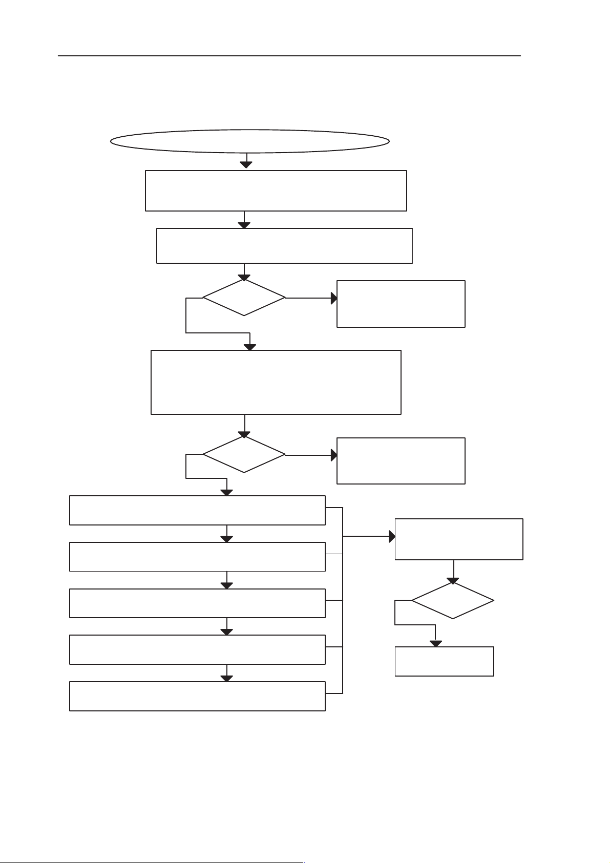
PAMS
RAE-3
Technical Documentation
2.23 BL8 related PDA UI problems
Problem with BL8
Put BL8 module in test jig, connect B–to–B adapter JC4.
DO NOT connect the UI module or Flex yet.
DO NOT switch power on.
Check the resistances of display signals to the GND (1)
Resistance > 1 MOhm ?
OK?
Connect the Flex and the UI module.
Turn the power on.
Check LCDDA0 to LCDDA11 signals at JC4 pin header.
Pins nos.5, 7, 19, 20, 22, 23, 24, 26, 36, 37, 38, 39
Constant activity, signal as in Fig 73?
NOYES
8. Troubleshooting
Check, replace
CSP filters Z401 to Z404
if voltage < 1MOhm
YES
NO
OK?
Check DispClk signal at pin 2. , use a min 1MOhm probe
Signal as in Fig, 77?
Check LLCLK signal at pin 40.
Signal as in Fig, 78?
Check FSP signal at pin 4.
Signal as in Fig, 79?
Check BackPWM signal at pin 31.
Signal as in Fig, 80?
Check LCDPWM signal at pin 10.
Signal as in Fig, 81?
Check, replace
CSP filters Z401 to Z404
if voltage = 0
Check, replace
CSP filters Z401 to Z404
YES
OK?
D300 or PWB faulty
Issue 1 06/01
Figure 65.
Page 8 – 79
Page 80

RAE-3
PAMS
8. Troubleshooting
Figure 66. LCDDA0–LCDDA11 signals on the pin header on JC4.
Technical Documentation
The pins are 5, 7, 19, 20, 22–24, 26, 36–39.
DispClk signal (Figure 67) at pin 2. Use at least 1MΩ probe for this.
Note: The more critical values are high 1.8V, frequency 8.645MHz and +Width
42ns. If the signal high time is too small, it will cause errors.
Page 8 – 80
Figure 67. DispClk signal at pin 2
Issue 1 06/01
Page 81
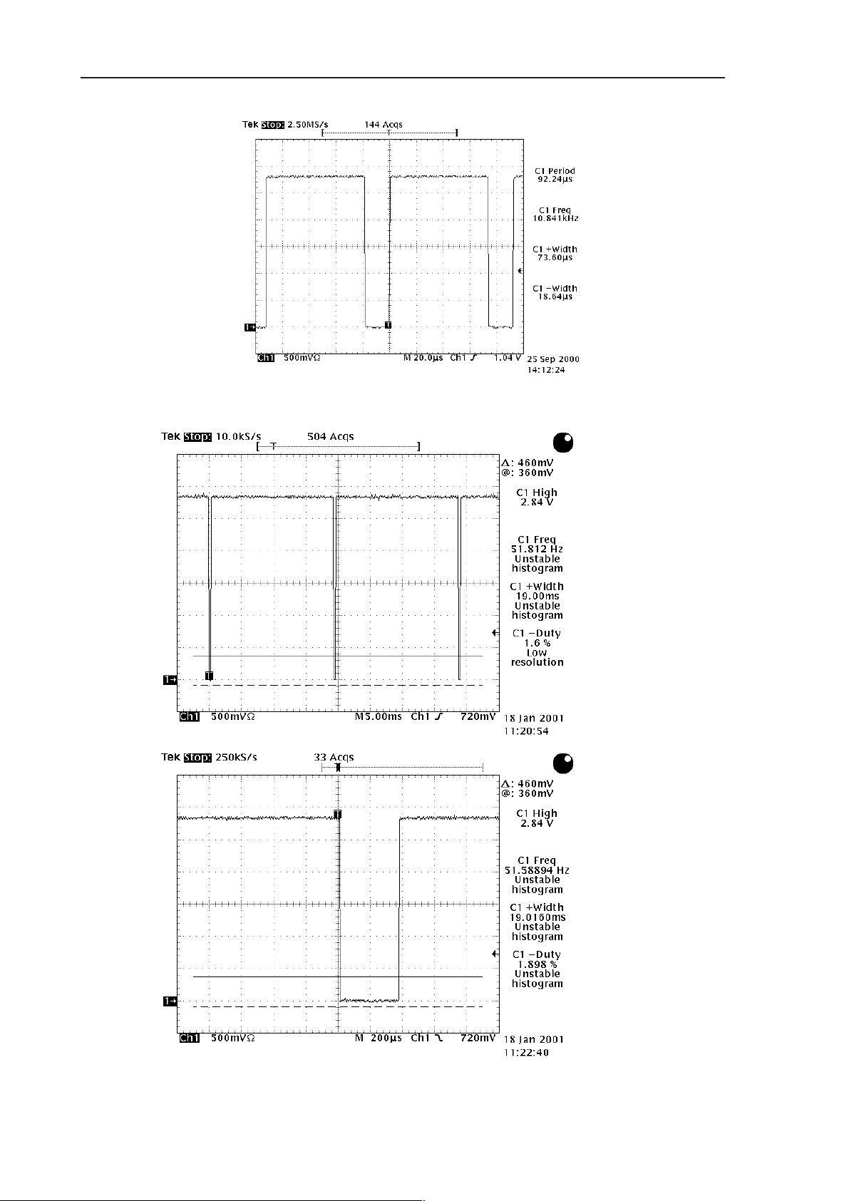
PAMS
RAE-3
Technical Documentation
8. Troubleshooting
Figure 68. LLCLK signal at pin 40.
Issue 1 06/01
Figure 69. FSP signal at pin 4.
Page 8 – 81
Page 82

RAE-3
PAMS
8. Troubleshooting
This signal (Figure 70) is a PWM control for display backlight. The pulse width
varies and is constant high for maximum intensity
Technical Documentation
Figure 70. BackPWM signal at pin 31
.
This signal (Figure 71) is a PWM control for display contrast. The pulse width
may vary significantly.
Table 3: List of display signals
Page 8 – 82
Figure 71. LCDPWM signal at pin 10.
Table 3. List of display signals
Display Signal JC4 pin no. Display Signal JC4 pin no.
LCDDa0 5 LCDDa10 39
LCDDa1 26 LCDDa11 7
LCDDa2 24 DispClk 2
LCDDa3 38 LLClk 40
LCDDa4 20 FSP 4
LCDDa5 36 DISPON 3
Issue 1 06/01
Page 83

PAMS
RAE-3
Technical Documentation
Table 3. (continued) List of display signals
LCDDa6 37 LCDM 18
LCDDa7 22 LCD_PWR 6
LCDDa8 19 LCDPWM 10
LCDDa9 23 BackPWM 31
Z400 Z401 Z402 Z403 Z404
DispClk LCDDa11 LCDM LCDDa1 BackPWM
LCDDa5 LCDPWM LCDDa8 LCDDa2
DISPON LCDDa4 LCDDa9
LCDDa6 LCDDa7
FSP
LCDDa3
LCDDa0
LCDDa10
LCD_PWR
LLClk
8. Troubleshooting
JC4 pin no.Display SignalJC4 pin no.Display Signal
Table 4. CSP filters and PDA UI signals
Issue 1 06/01
Page 8 – 83
Page 84

RAE-3
PAMS
8. Troubleshooting
2.24 BL8 related CMT UI problems
Problem with CMT UI
Put BL8 module in test jig, connect B–to–B adapter JC4.
DO NOT connect the UI module or Flex yet.
DO NOT switch power on.
Check the resistances of display signals to the GND (1)
Resistance > 1 MOhm, GENSDIO = 47kOhm?
OK?
Connect the Flex and the UI module.
Turn the power on.
Check GENSCLK, signal as in Fig. 80 ?
NOYES
Technical Documentation
Check, replace
CSP filter Z401
YES
OK?
Check GENSDIO siglnal while LCDEN is active.
Rise/fall time: 30 to 60 ns?
Check LCDEN signal.
Rise/fall time: 30 to 60 ns?
Check LCDRSTX signal
Signal 2.8 V or active?
NO
Figure 72.
Check, replace
CSP filter Z401
if voltage = 0
NO
YES
Check, replace
CSP filter Z401
OK?
D300 or PWB faulty
Page 8 – 84
Issue 1 06/01
Page 85

PAMS
RAE-3
Technical Documentation
8. Troubleshooting
Figure 73. GENSCLK signal.
GENSCLK signal (Figure 73 ). It should look like this when LCDEN signal is active. There is also a 2.16MHz clock signal, but it is targeted for CCONT.
Table 5. Signals and pins
Signal Pin no.
LCDEN 12
GENSDIO 9
GENSCLK 11
LCDRSTX 14
Table above: Signals and corresponding pins.
Issue 1 06/01
Page 8 – 85
Page 86

RAE-3
PAMS
8. Troubleshooting
3 DL2 UI Troubleshooting
3.1 CMT and keypad illumination problems
Each CMT–display and keypad LED has its own driver. If there is problems with
one or more
– Keypad–LED: check resistors R203–R208, transistors V213, V203, V204 and
the LEDs.
– CMT–LED: check resistors R200–R202, transistor V206 and the LEDs.
If the illumination does not work at all, measure voltages VB and KBLIGHTS.
VB should be the same as VBATT and KBLIGHTS approximately 2.5V when
the LEDs are supposed to be on. If these voltages are not correct, problem is in
hinge flex, connector X001 or on BL8 (see 2.23 in this document).
3.2 CMT LCD Troubleshooting
CMT LCD
faulty
Technical Documentation
Check
C002, R003, X007
Make sure that the display flex is
connected to X007
NO
CMT LCD or LCD Flex
probably damaged
NO
Display
OK?
Replace LCD.
Display
OK?
YES
YES
END
Page 8 – 86
Hinge Flex, connector X001
Problem in
or BL8
Refer to chapter
2.23
Figure 74.
Issue 1 06/01
Page 87

PAMS
RAE-3
Technical Documentation
3.3 No picture on PDA LCD or picture is faulty
To start with, check that the flex connector (X001) from BL8 to UL2 is connected properly and that soldering joints are ok.
Check also connectors X002 and X003. Check that PDA display is not mechanically damaged, i.e. pixels missing.
8. Troubleshooting
Issue 1 06/01
Page 8 – 87
Page 88

RAE-3
PAMS
8. Troubleshooting
Start Section 1
Picture on
LCD?
NO
See Section 3
Measure
V5Y_1,
should be
appr.–15V
See Section: bl8
related PDA UI
problems
Check
components
R063 and R070
NO V5Y_1 0V?
ON
Measure
NO
NO
BRIGHT
(Fig.81)
YES
Measure
SET , should
be 1.4V
OK?
Technical Documentation
Measure
YES
ST_INVOUT
(Fig.79)
OK?
ON
Measure
DD_P1
(Fig.80)
OK?OK?
ON
Display ASIC
fault(D054)
YES
YES
Check components
L050, C068, V062
and V069
Check
components C058
and R075
YES
Check test
patterns
with
WInTesla
OK?
YES
Check
components
R068, R072,
R077 and V056
NO
NO
YES
Measure
CONT ,
should be
400mV
OK?
YES
Measure
TEMP,
should be
850mV
OK?
YES
Measure
FB, should
be 900mV
OK?
See Section 2
YES
NO
NO
Check
components
V055 and V058
Check
components
R066, V061,
R067, R076,
V066, R078 and
R081
YES
LCD OK!
Page 8 – 88
Figure 75.
Issue 1 06/01
Page 89
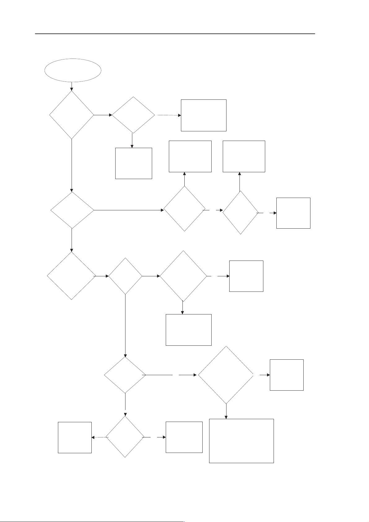
PAMS
RAE-3
Technical Documentation
Start Section 2
Measure
V5Y(Fig.85)
and VCCY
(Fig.86)
OK?
YES
Measure
VOY(Fig.85)
OK?
NO
Measure
FRYS(Fig.84)
OK?
NO
Display ASIC
fault
NO
YES
components
between FRYS,
V5Y and VCCY
Check
components
V060, R079 and
C064
YES
Measure
VDD, it
should be
~3.8V
OK?
Check
NO
Check
components
C076,V072,
N050, C075 and
C101
YES
Measure
DD_P2
(Fig.86)
OK?
8. Troubleshooting
NO
Display ASIC
fault
YES
Measure
DY(Fig.90)
FRY(Fig.91)
YSCL(Fig.92)
XINH(Fig.93)
DY OK?
YES
FRY, YSCL,
XINH OK?
YES
NO
Measure
DY_A
(Fig.91) and
XSET(should
be 2.8V)
OK?
YES
Check
components
V050,R051,R050
, V052,
R053,D050,V051
R055
NO
NO
FRY_A (fig.92)
YSCL_A (fig.93)
and
Display ASIC
Measure
XINH_A
(2.8V) OK?
YES
fault
NO
Display ASIC
fault
See section 4
Issue 1 06/01
YES
Measure
XSCL
(Fig.94)
OK?
Figure 76.
NO
Display ASIC
fault
Check
components
C051,R054,R052,
D050, C052, D051
D052, R056, V053
V054, C054, C055
R059, R064, R058, R061
Page 8 – 89
Page 90
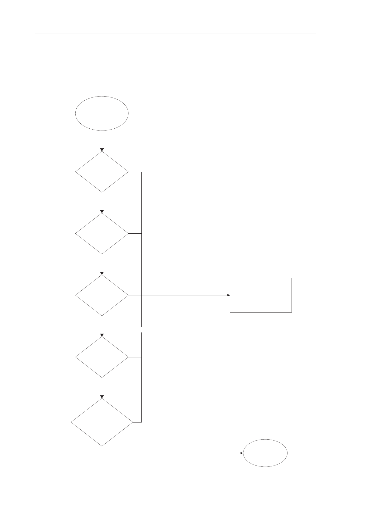
RAE-3
PAMS
8. Troubleshooting
NOTE!! See section 2.23. There are all the relevant pictures of the signals
mentioned below. Measure these signals from UL2 side. This is to make sure
that the problem is not in BL8 side.
Start Section 3
Measure
DispClk(J012),
Technical Documentation
OK?
YES
Measure
LLClk(J027),
OK?
YES
Measure
FSP(J020),
OK?
YES
Measure
DISPON(J021),
2.8V?
YES
Measure
LCDDA0–
A2,A4,A7–
A9,A11(J019,J002
,J004,J007,J006,J
008,J005,J017),
OK?
NO
NO
See section bl8 related
PDA UI problems
Page 8 – 90
Figure 77.
YES
Return to section
1
Issue 1 06/01
Page 91
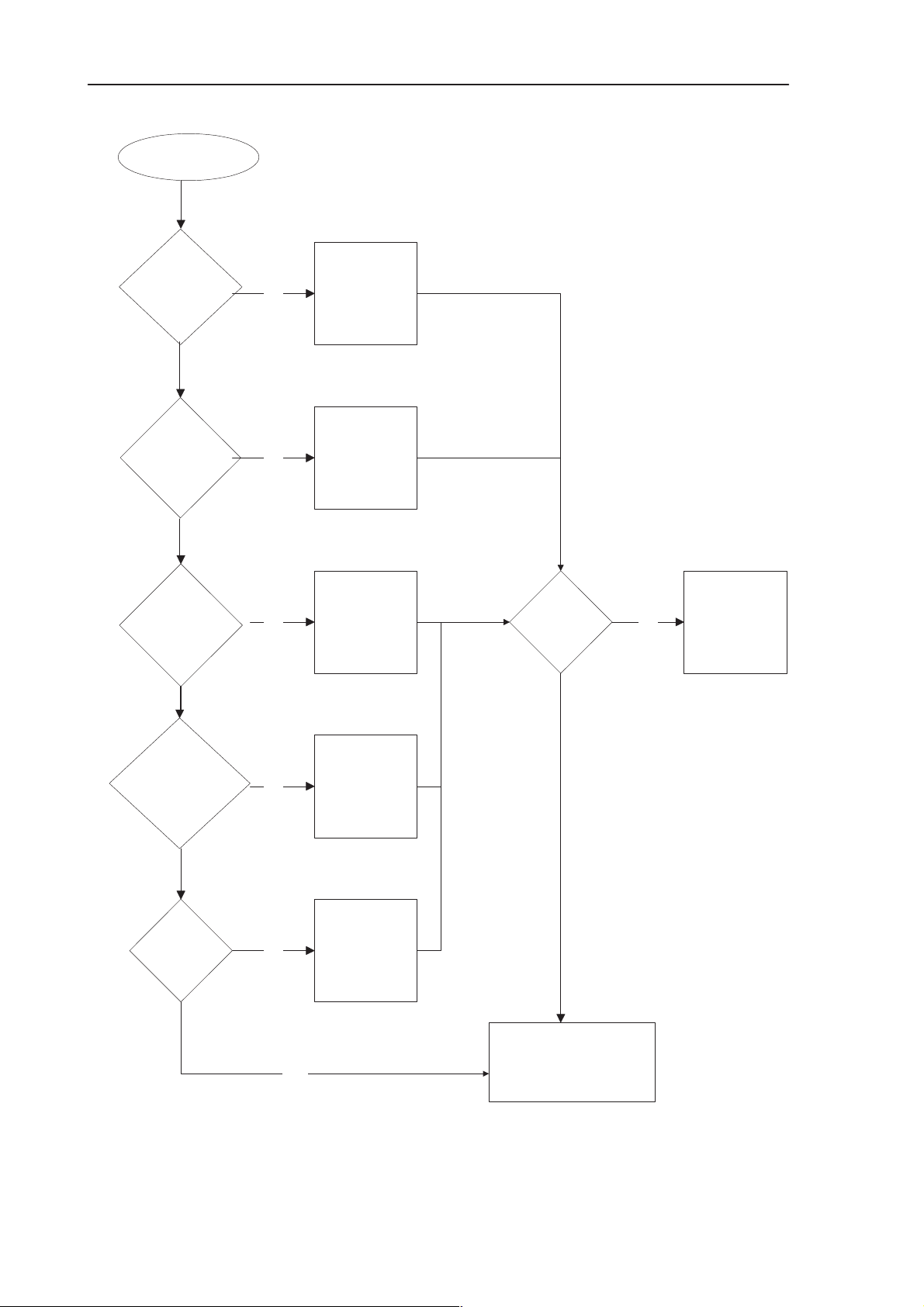
PAMS
RAE-3
Technical Documentation
Start Section 4
Measure
D10,D11,
D12 and
D13(Fig.98)
OK?
YES
Measure
D00,D01,
D02 and
D03(Fig.98)
OK?
YES
NO
NO
8. Troubleshooting
Check
component R087
Check
component R088
Measure
D20,D21,
D22 and
D23(Fig.98)
OK?
Measure
RES,LP and
GOP
(Figs.99, 100,
101 )
OK?
YES
Measure FR
(Fig.102)
OK?
YES
NO
NO
NO
Check
component R090
Check
component R089
Check
component R091
Signals OK?
YES
NO
Display
ASIC(D054) fault
Issue 1 06/01
YES
Figure 78.
Display module fault
Page 8 – 91
Page 92

RAE-3
PAMS
8. Troubleshooting
Technical Documentation
Figure 79. ST_INVOUT signal
Page 8 – 92
Figure 80. DD_P1 signal
Figure 81. BRIGHT signal
Issue 1 06/01
Page 93
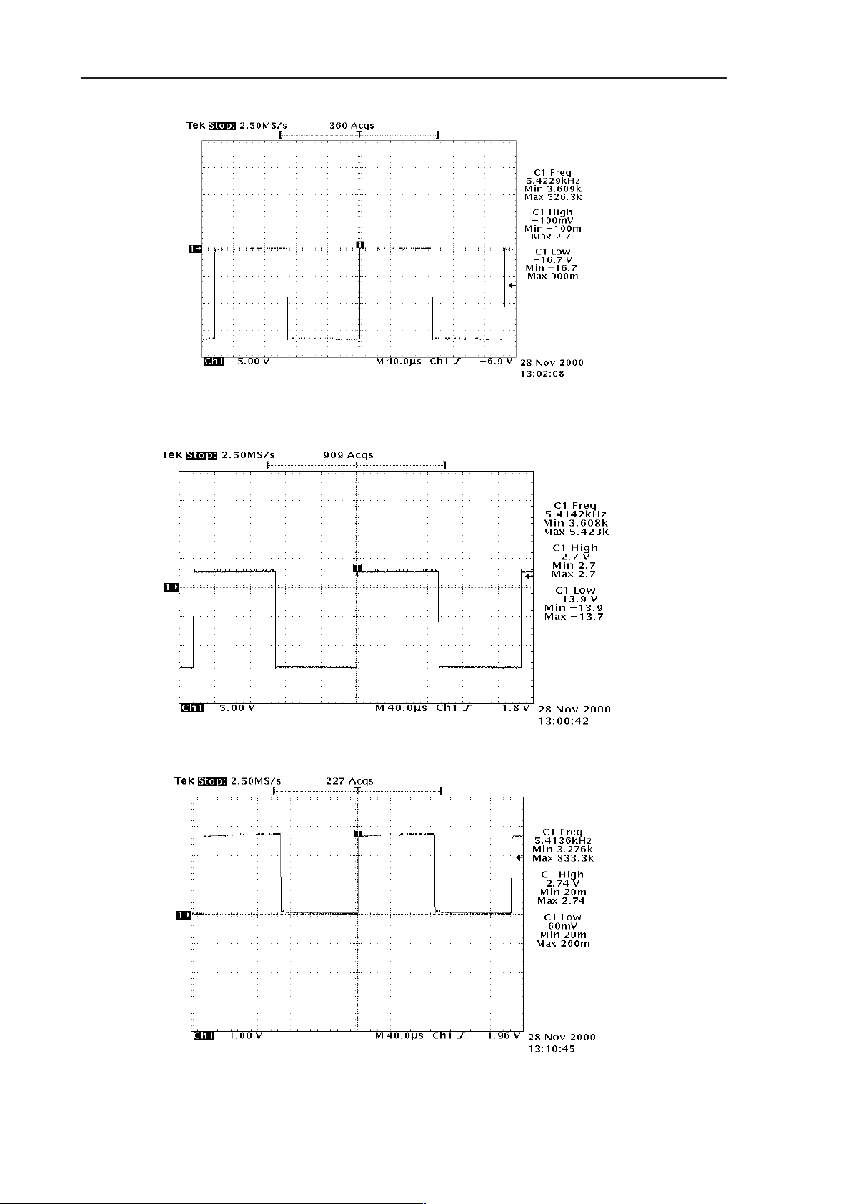
PAMS
RAE-3
Technical Documentation
8. Troubleshooting
Figure 82. V5Y signal
Issue 1 06/01
Figure 83. VCCY signal
Figure 84. FRYS signal
Page 8 – 93
Page 94
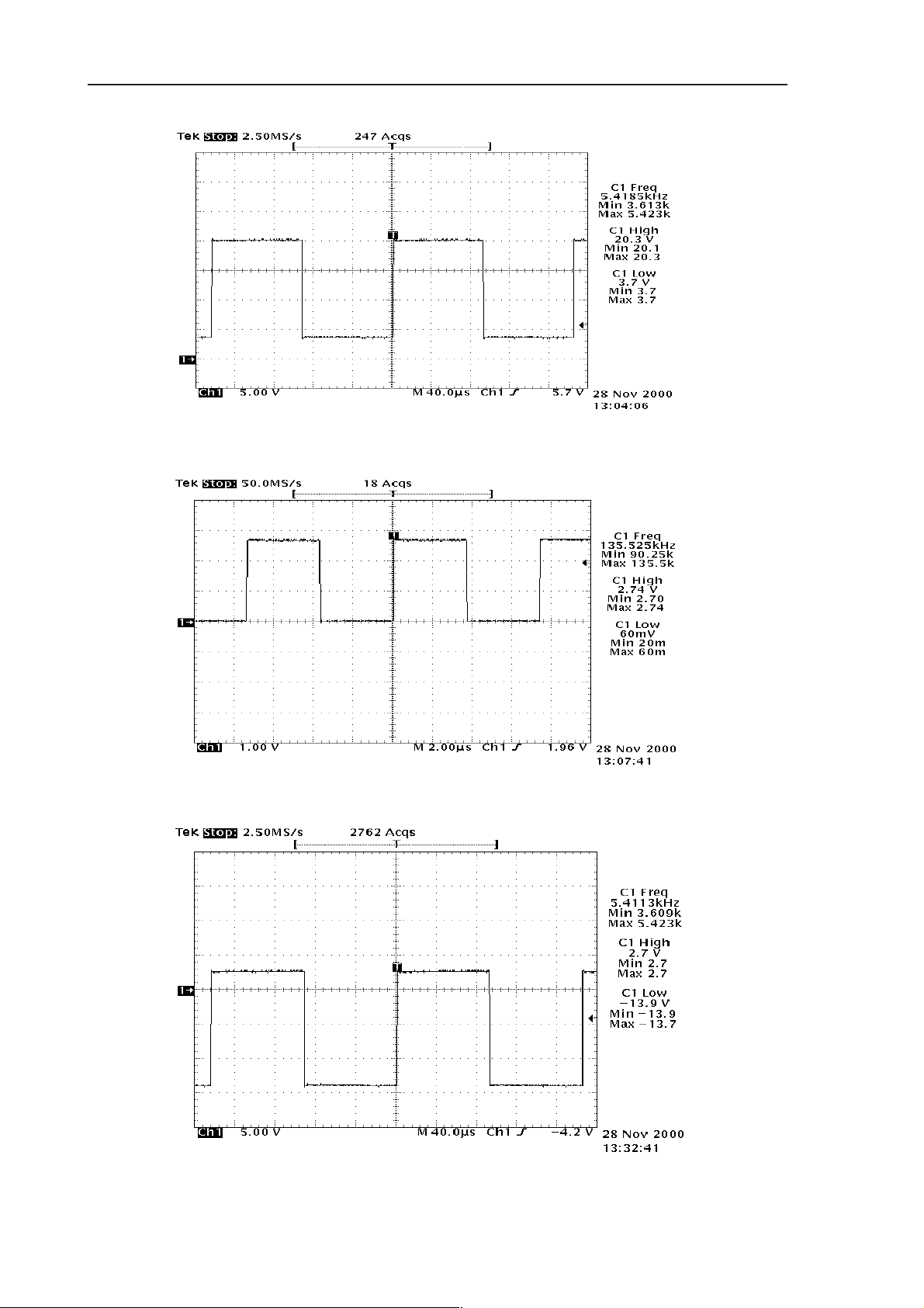
RAE-3
PAMS
8. Troubleshooting
Technical Documentation
Figure 85. VOY signal
Figure 86. DD_P2 signal
Figure 87. DY signal
Page 8 – 94
Issue 1 06/01
Page 95
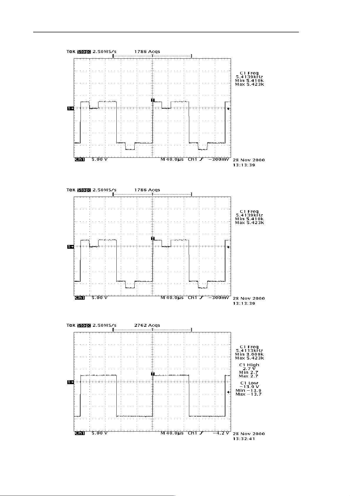
PAMS
RAE-3
Technical Documentation
8. Troubleshooting
Figure 88. FRY signal
Issue 1 06/01
Figure 89. YSCL signal
Figure 90. XINH signal
Page 8 – 95
Page 96

RAE-3
PAMS
8. Troubleshooting
Technical Documentation
Figure 91. DY_A signal
Page 8 – 96
Figure 92. FRY_A
Figure 93. YSCL_A signal
Issue 1 06/01
Page 97

PAMS
RAE-3
Technical Documentation
8. Troubleshooting
Figure 94. XSCL signal
(Note!! There should be constant activity in the datalines and signals should
look something like this.)
Issue 1 06/01
Figure 95. Data signal
Page 8 – 97
Page 98

RAE-3
PAMS
8. Troubleshooting
Technical Documentation
Figure 96. RES signal
Page 8 – 98
Figure 97. GOP signal
Issue 1 06/01
Page 99

PAMS
RAE-3
Technical Documentation
8. Troubleshooting
Figure 98. LP signal
Issue 1 06/01
Figure 99. FR signal
Page 8 – 99
Page 100
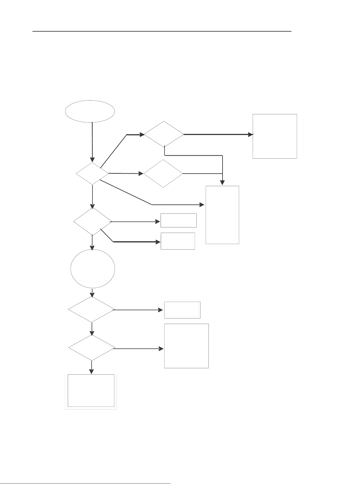
RAE-3
PAMS
8. Troubleshooting
3.4 Backlight troubleshooting
NOTE: when making measurements, make sure that BACK_PWM is 100%
No PDA
backlight
Measure
VCO_OUT
Check V152
and R158
Measure
95–1 10 kHz
Measure
PIEZO_IN
95–1 10 kHz
No signal
150–180kHz
DRAIN
No signal
Square wave
Else
Still fails
Other frequency
Check L151
Check PIEZO
and X006
Technical Documentation
Between 95kHz and 180kHz
Check VCO
components:
R174, V156,
C173, C172,
N153, R175,
R179, R178,
R177, R176,
D155 and
R160
Check components:
D150, D151, R156,
R150, ,
R172, R151
R157, R169, V150,
V151, and L150
Feed 1.2VDC
to VCO_IN.
Now frequency
of DRAIN should
be 135kHz
Measure
FEEDBACK
OK?
Yes
Measure
SIGN
OK?
Yes
Check components:
N151, R154, C170,
R161, R162, N152,
R159, D154, R155,
C153, V152, R168
No
No
Check lamp
and R158
Check components:
C154, R165, R166,
R153, R171,R164,
R180, R170, R163,
N152, D152, R173,
C169, R152, V155
Page 8 – 100
Figure 100.
Issue 1 06/01
 Loading...