

Page 1

PAMS Technical Documentation
RAE-3 Series PDA
9. Schematic diagrams
Issue 1 05/01
Copyright 2001. Nokia Mobile Phones. All Rights Reserved.
Page 2
RAE-3
PAMS
9. Schematic diagrams
Amendment
Number
Date Inserted By Comments
06/01 OJuntunen
Technical Documentation
AMENDMENT RECORD SHEET
Page 12 – 2
Issue 1 05/01
Page 3

PAMS
RAE-3
Technical Documentation
9. Schematic diagrams
CONTENTS –Troubleshooting
Block Diagram of FL1_08 QWERTY keypad
(Version 0.0 Edit 37) 12 – 4. . . . . . . . . . . . . . . . . . . . . . . . . . . . . . . . . . . .
Block Diagram of FL1_08 QWERTY and Hinge flex
(Version 0.0 Edit 27) 12 – 5. . . . . . . . . . . . . . . . . . . . . . . . . . . . . . . . . . . .
Circuit Diagram of UL2_21 CMT keypad and PDA Soft keys
(Version 0.0 Edit 20) 12 – 6. . . . . . . . . . . . . . . . . . . . . . . . . . . . . . . . . . . .
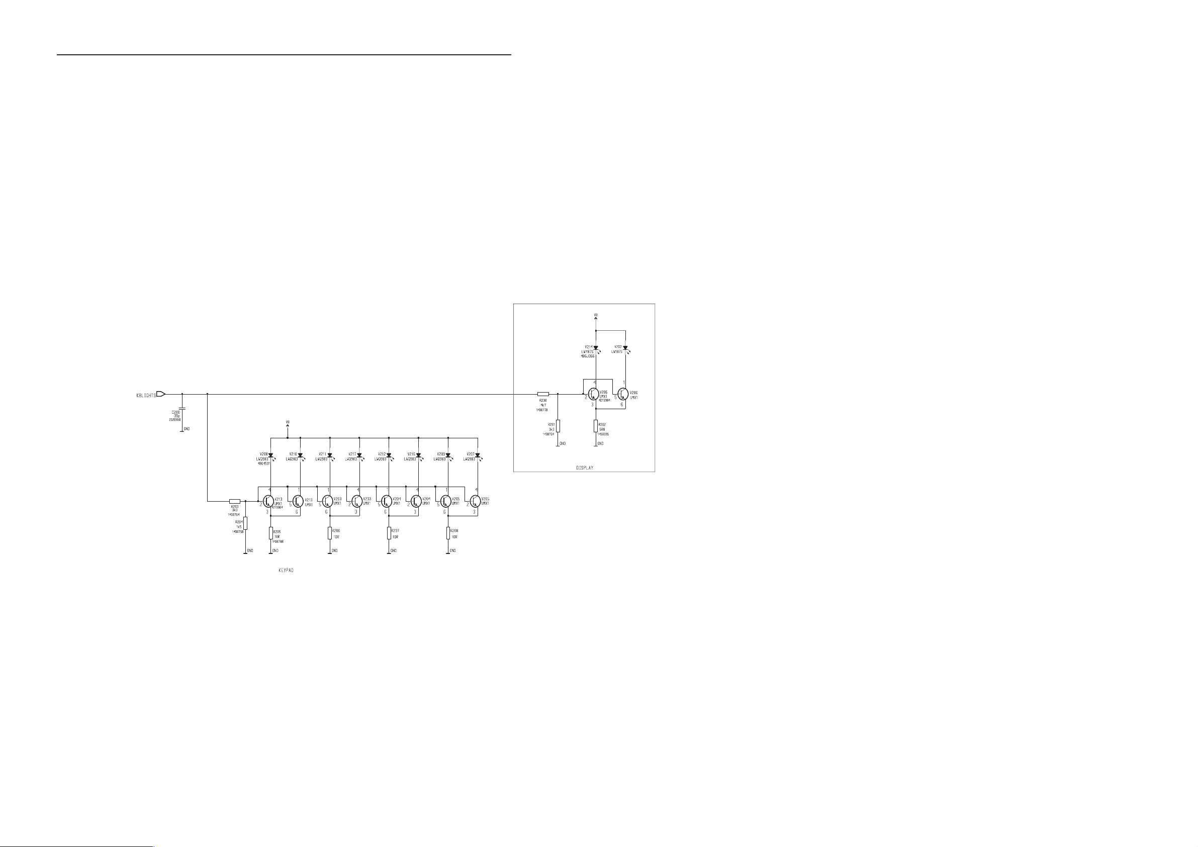
Circuit Diagram of UL2_21 CMT UI LEDs (Version 0.0 Edit 28) 12 – 7
Circuit Diagram of UL2_21 CCFL power (Version 0.0 Edit 28) 12 – 8.
Circuit Diagram of UL2_21 PDA driver (Version 0.0 Edit 28) 12 – 9. .
Block Diagram of BL8_18 System (Version 0.0 Edit 40) 12 – 10. . . . . .
Circuit Diagram of BL8_18 System Conn (Version 0.0 Edit 117) 12 – 11
Circuit Diagram of BL8_18 Audio RFI (Version 0.0 Edit 136) 12 – 12. .
Page No
Circuit Diagram of BL8_18 CPU (Version 0.0 Edit 155) 12 – 13. . . . . . .
Circuit Diagram of BL8_18 IRDA (Version 0.0 Edit 77) 12 – 14. . . . . . .
Circuit Diagram of BL8_18 memories (Version 0.0 Edit 87) 12 – 15. . .
Circuit Diagram of BL8_18 MMC (Version 0.0 Edit 65) 12 – 16. . . . . . .
Circuit Diagram of BL8_18 Power (Version 0.0 Edit 204) 12 – 17. . . . .
Circuit Diagram of BL8_18 User interface
(Version 0.0 Edit 136) 12 – 18. . . . . . . . . . . . . . . . . . . . . . . . . . . . . . . . . . .
Circuit Diagram of BL8_18 RF/BB
Connector (Version 1.0 Edit 55) 12 – 19. . . . . . . . . . . . . . . . . . . . . . . . . . .
Circuit Diagram of BL8_18 RF (Version 0.0 Edit 136) 12 – 20. . . . . . . .
Parts Placement Diagram of BL8_18 1/2 12 – 21. . . . . . . . . . . . . . . . . .
Parts Placement Diagram of BL8_18 2/2 12 – 22. . . . . . . . . . . . . . . . . .
BL8 Test Points v. 18 1/2 12 – 23. . . . . . . . . . . . . . . . . . . . . . . . . . . . . . . . .
BL8 Test Points v. 18 1/2 12 – 24. . . . . . . . . . . . . . . . . . . . . . . . . . . . . . . . .
UL2 Test Points v. 21 12 – 25. . . . . . . . . . . . . . . . . . . . . . . . . . . . . . . . . . . .
Issue 1 05/01
Page 12 – 3
Page 4
RAE-3
PAMS
9. Schematic diagrams
Technical Documentation
Block Diagram of FL1_08 QWERTY keypad (Version 0.0 Edit 37)
Page 12 – 4
Issue 1 05/01
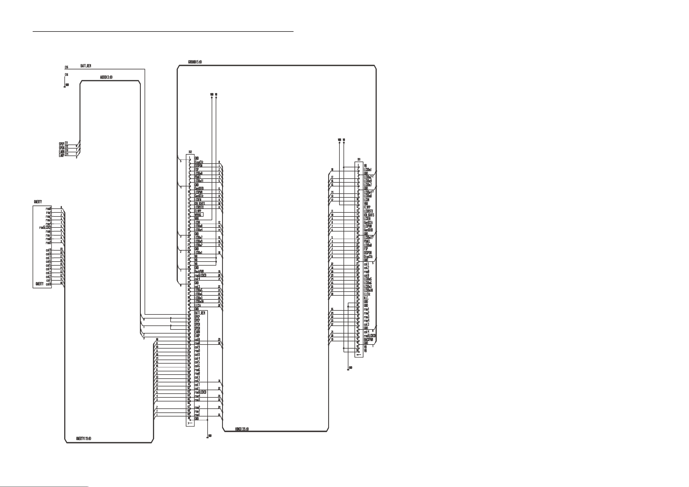
Page 5
PAMS
RAE-3
Technical Documentation
9. Schematic diagrams
Block Diagram of FL1_08 QWERTY and Hinge flex (Version 0.0 Edit 27)
Issue 1 05/01
Page 12 – 5
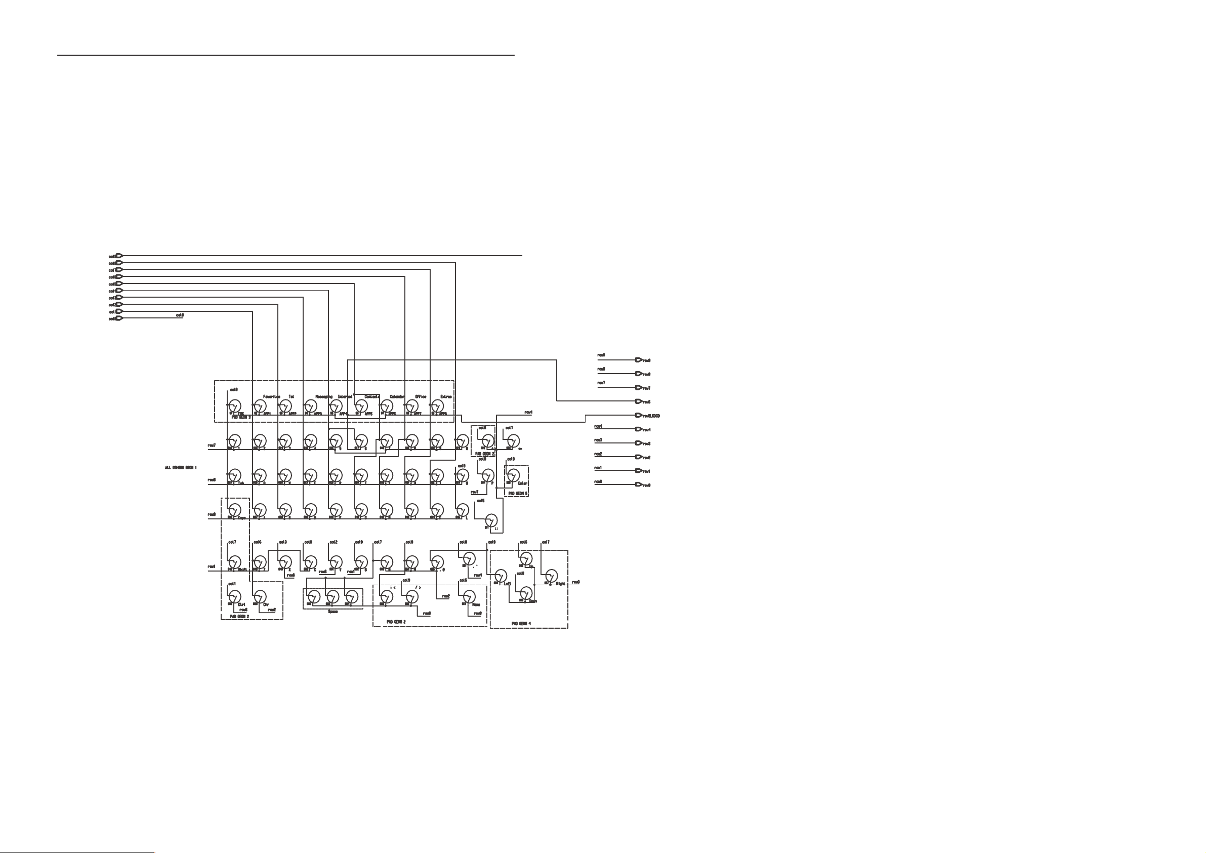
Page 6
RAE-3
PAMS
9. Schematic diagrams
Technical Documentation
Circuit Diagram of UL2_21 CMT keypad and PDA Soft keys (Version 0.0 Edit 20)
Page 12 – 6
Issue 1 05/01
Page 7
PAMS
RAE-3
Technical Documentation
Circuit Diagram of UL2_21 CMT UI LEDs (Version 0.0 Edit 28)
9. Schematic diagrams
Issue 1 05/01
Page 12 – 7
Page 8
RAE-3
PAMS
9. Schematic diagrams
Technical Documentation
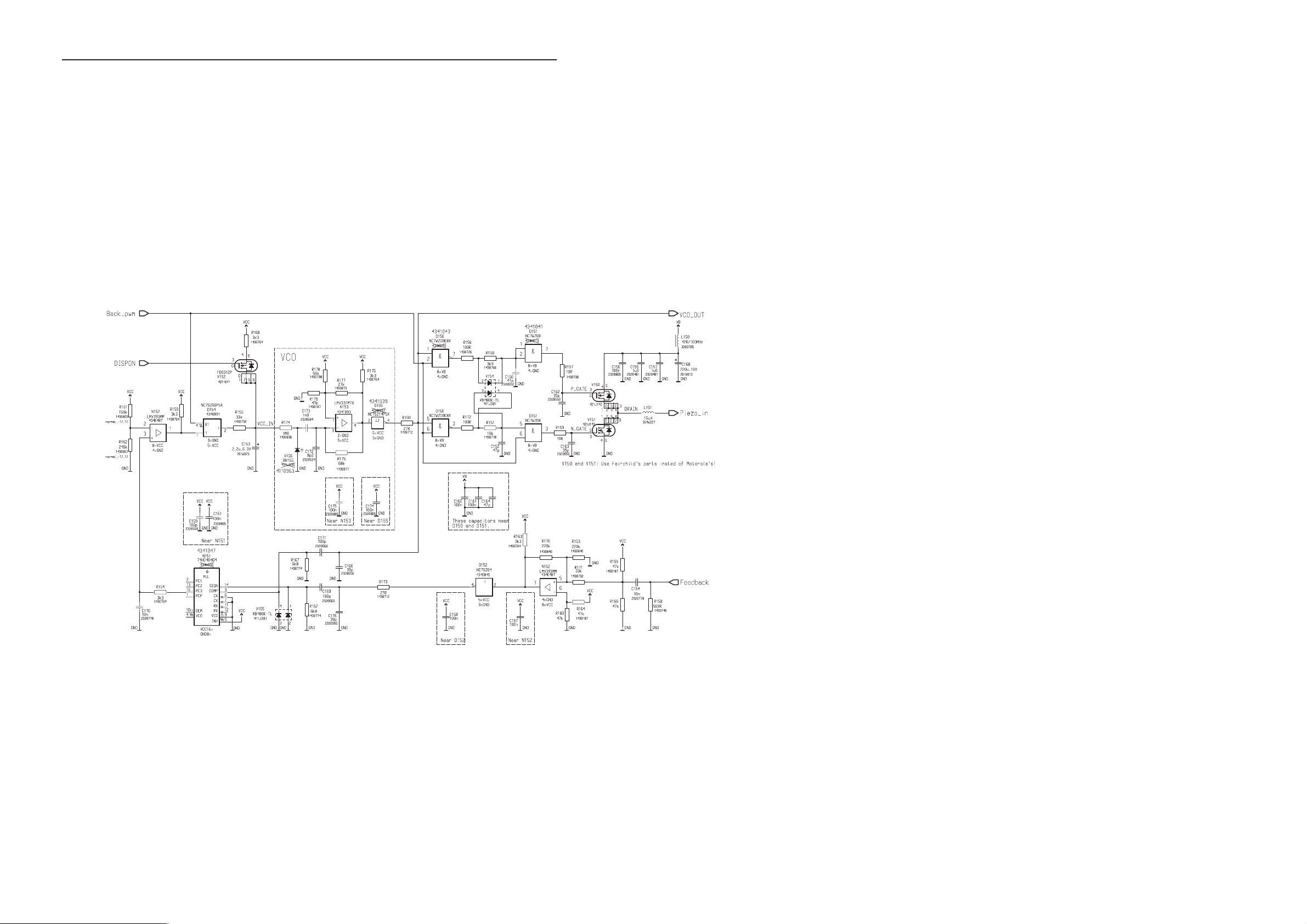
Circuit Diagram of UL2_21 CCFL power (Version 0.0 Edit 28)
Page 12 – 8
Issue 1 05/01
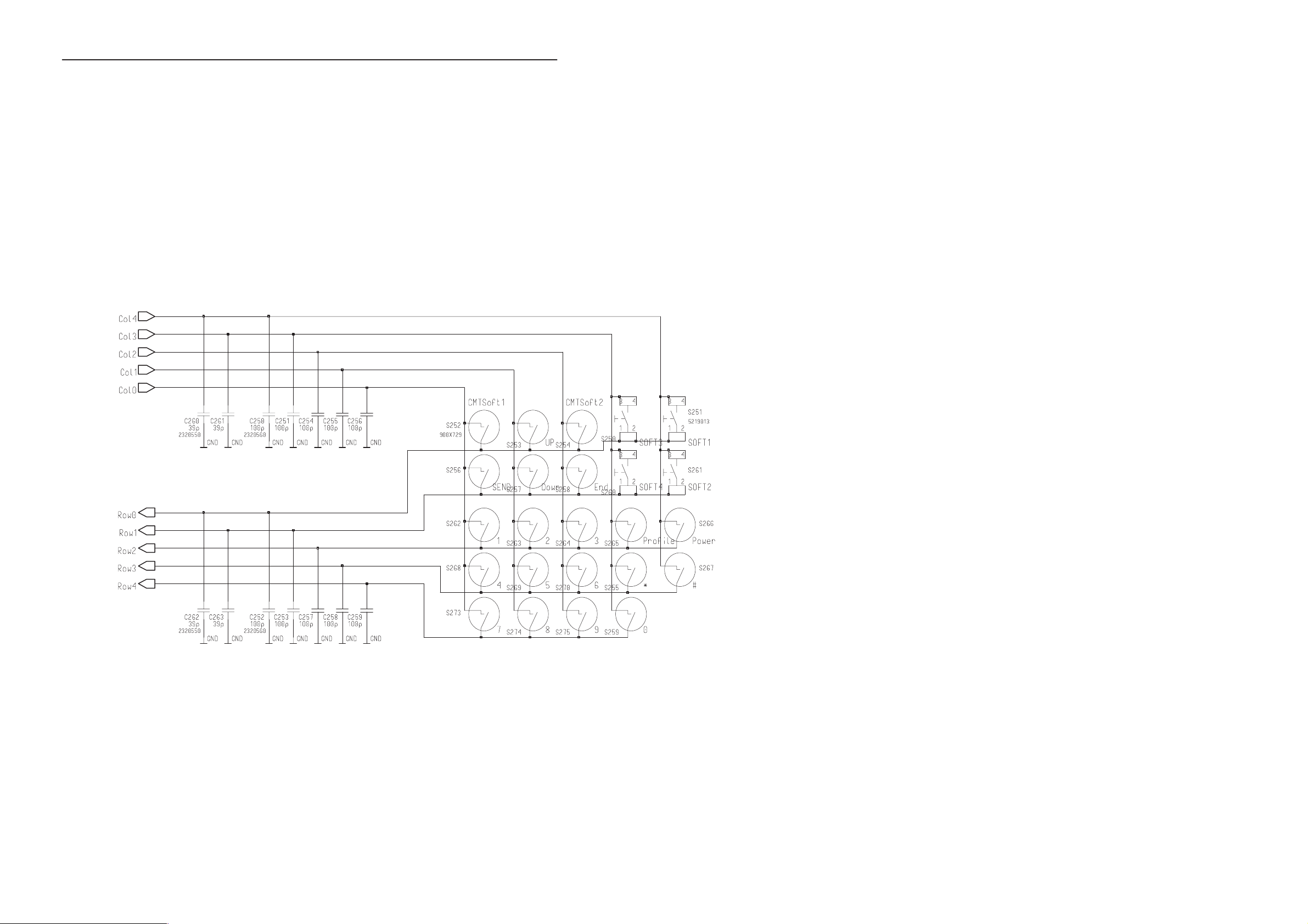
Page 9
PAMS
RAE-3
Technical Documentation
Circuit Diagram of UL2_21 PDA driver (V ersion 0.0 Edit 28)
9. Schematic diagrams
Issue 1 05/01
Page 12 – 9
Page 10

RAE-3
PAMS
9. Schematic diagrams
Block Diagram of BL8_18 System (Version 0.0 Edit 40)
Technical Documentation
Page 12 – 10
Issue 1 05/01
Page 11

PAMS
RAE-3
Technical Documentation
9. Schematic diagrams
Circuit Diagram of BL8_18 System Connector (Version 0.0 Edit 117)
BL8_18 syscon
Issue 1 05/01
Page 12 – 11
Page 12

RAE-3
PAMS
9. Schematic diagrams
Technical Documentation
Circuit Diagram of BL8_18 Audio RFI (Version 0.0 Edit 136)
Linda HP3.1
BL8_18 audio_rfi
Page 12 – 12
Issue 1 05/01
Page 13

PAMS
RAE-3
Technical Documentation
Circuit Diagram of BL8_18 CPU (Version 0.0 Edit 155)
9. Schematic diagrams
BL8_18 cpu
Linda HP3.1
Issue 1 05/01
Page 12 – 13
Page 14

RAE-3
PAMS
9. Schematic diagrams
Circuit Diagram of BL8_18 IRDA (Version 0.0 Edit 77)
Technical Documentation
Page 12 – 14
Issue 1 05/01
Page 15

PAMS
RAE-3
Technical Documentation
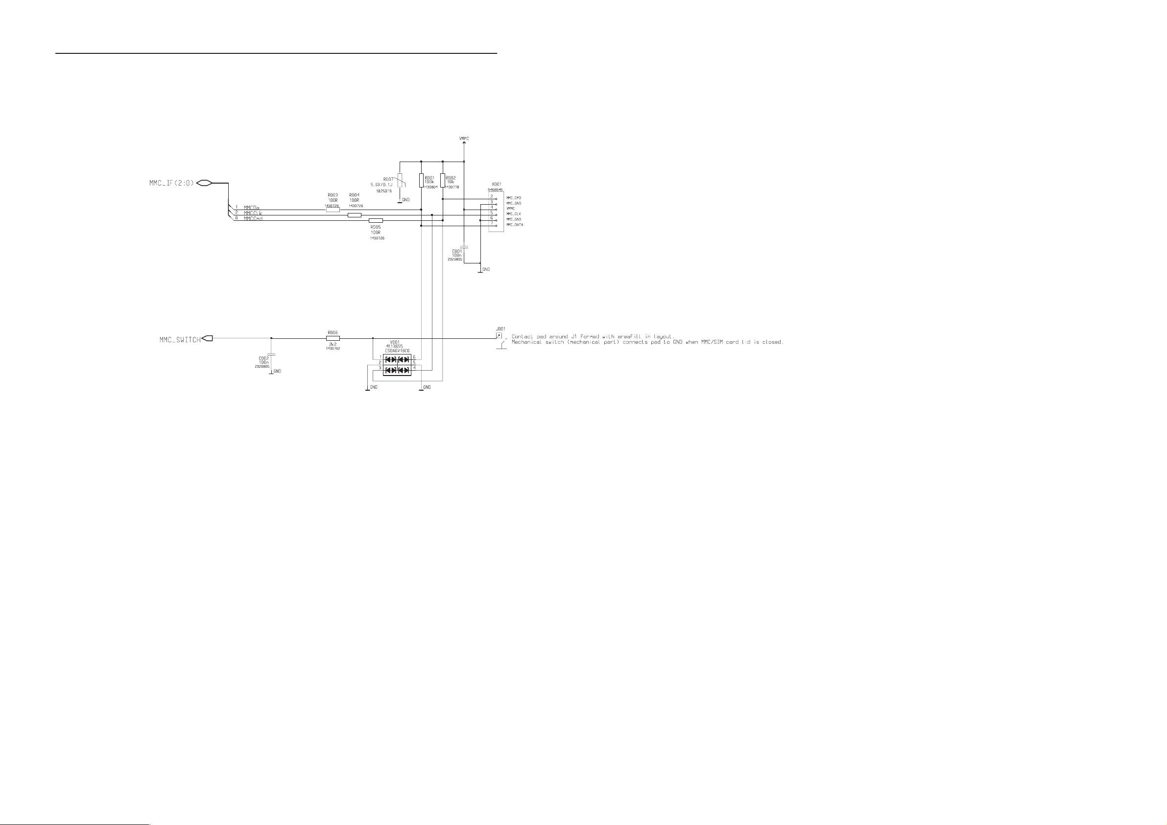
Circuit Diagram of BL8_18 memories (Version 0.0 Edit 87)
9. Schematic diagrams
Linda HP3.1
BL8_18 memories
Issue 1 05/01
Page 12 – 15
Page 16
RAE-3
PAMS
9. Schematic diagrams
Circuit Diagram of BL8_18 MMC (Version 0.0 Edit 65)
Technical Documentation
Page 12 – 16
Issue 1 05/01
Page 17
PAMS
RAE-3
Technical Documentation
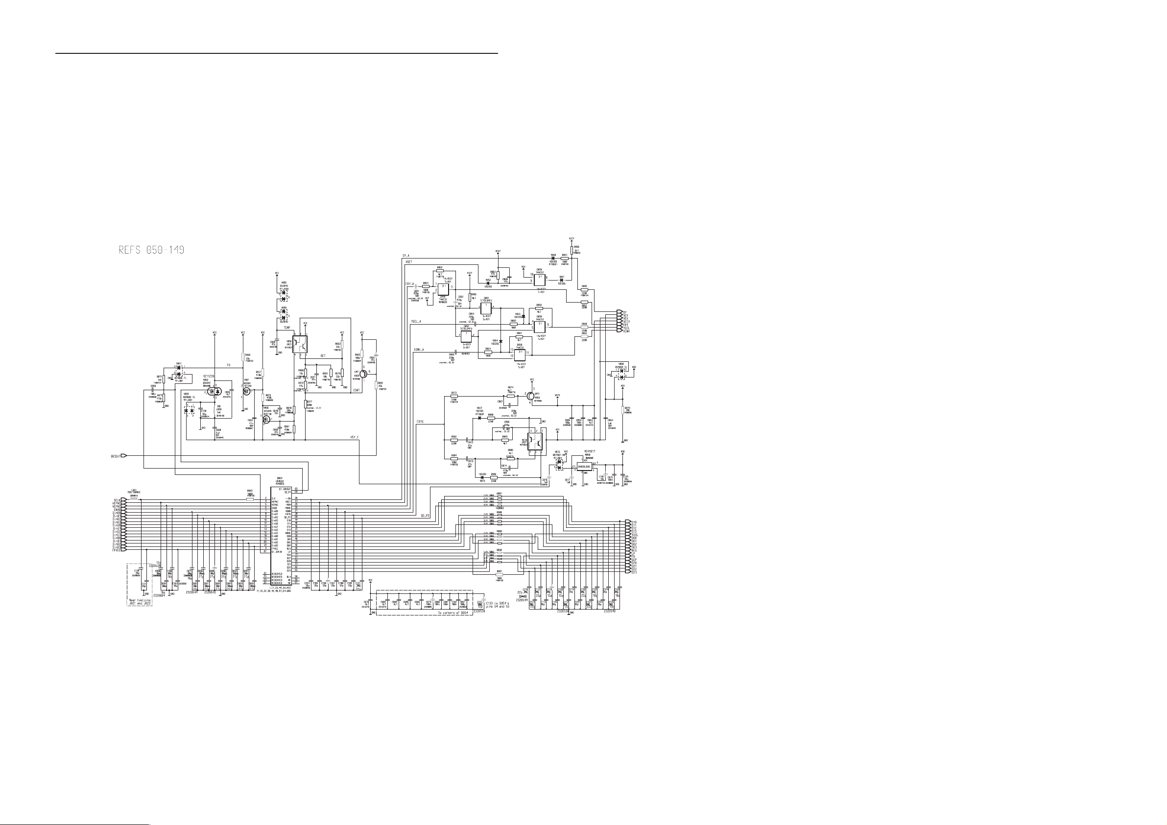
Circuit Diagram of BL8_18 Power (Version 0.0 Edit 204)
9. Schematic diagrams
BL8_18 power
Not assembled
Not assembled
Issue 1 05/01
Page 12 – 17
Page 18

RAE-3
PAMS
9. Schematic diagrams
Technical Documentation
Circuit Diagram of BL8_18 User interface (Version 0.0 Edit 136)
Page 12 – 18
Issue 1 05/01
Page 19
PAMS
RAE-3
Technical Documentation
9. Schematic diagrams
Circuit Diagram of BL8_18 RF/BB Connector (Version 1.0 Edit 55)
Issue 1 05/01
Page 12 – 19
Page 20
RAE-3
PAMS
9. Schematic diagrams
Circuit Diagram of BL8_18 RF (Version 0.0 Edit 136)
LAYER_4
LAYER_4
Technical Documentation
Wide connection
below component
LAYER_4
Wide connection
below component
Not assembled
Not assembled
Not assembled
Not assembled
Not assembled
Not assembled
Not assembled
Not assembled
Not assembled
Wide connection
below component
Wide connection
below component
Not assembled
Not assembled
Not assembled
Charge pump
TOO HIGH VOLT
Modulator
VCTCXO
LNA2+mixer+DTOS
Dividers+LO–buffers+prescaler+VCO
Vdd_bb+LNA
Page 12 – 20
Not assembled
Issue 1 05/01
Page 21
PAMS
RAE-3
Technical Documentation
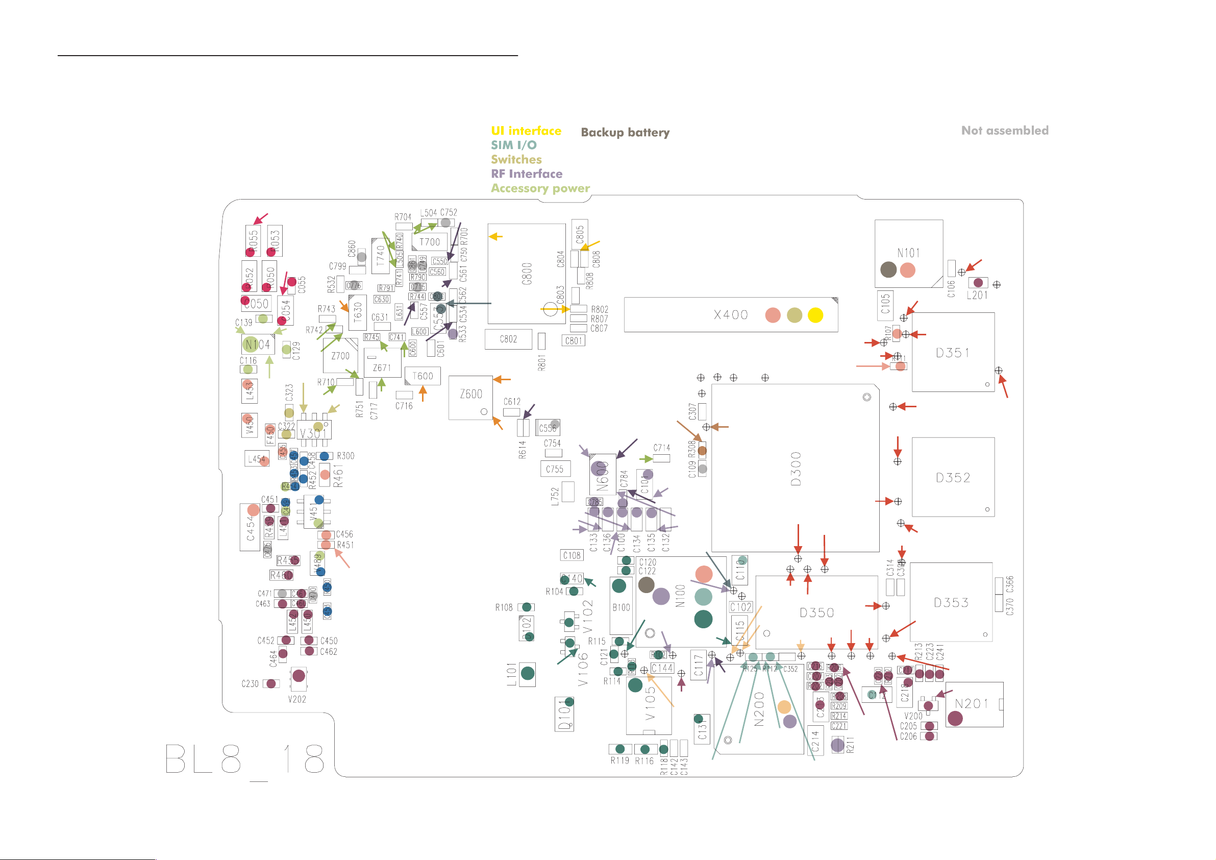
Parts Placement Diagram of BL8_18 1/2
9. Schematic diagrams
Issue 1 05/01
Page 12 – 21
Page 22
RAE-3
PAMS
9. Schematic diagrams
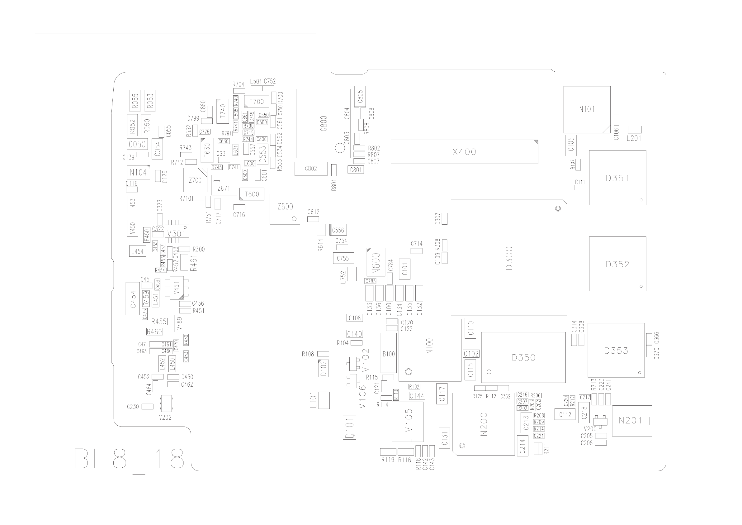
Parts Placement Diagram of BL8_18 2/2
Technical Documentation
Page 12 – 22
Issue 1 05/01
Page 23
PAMS
RAE-3
Technical Documentation
BL8 Test Points v. 18 1/2
Pin 5 of N102
Serial Flash
VB
FLVPP
9. Schematic diagrams
J337
J346
HOOKDET
J328
VBB
BSI
Memory Card Connector
RFClk
SLEEPCLK
J501
J502
69
71
70
1
2
LID_SWITCH
32
J500
J317
PCMDClk
7
68
8
1
2
6
IRDI (Rxd)
VBB (VCC)
IREN (Sd)
58
9
3
IRDO (Txd)
IRED_A
6
5
4
3
1
64
66
67
RFC
OSC_IN
58
22
25
46
Spring contacts
54
34
55
17
45
14
35
47
36
48
Audio & PCM
CCONT serial interface
Charging
Clocks
COBBA serial interface
SIM_CLK_CARDSIDE
SIM_RESET_CARDSIDE
SIM_DATA_CARDSIDE
MBIAS
J001
IRDA
Memory
MMC
Power
Serial
MMCDa
VSIM
VCOBBA
MMC_SWITCH
PCMSClk
AGND
AUXOUT
PCMRxData
SIM_CLK_O
MMCClk
MMCCmd
50
38
VCORE
21
33
4
VAMP
19
20
13
12
RX
RF power
VCO and IQ
TX
11
10
Issue 1 05/01
Page 12 – 23
Page 24
RAE-3
PAMS
9. Schematic diagrams
BL8 Test Points v. 18 1/2
Audio & PCM
CCONT serial interface
Charging
Clocks
COBBA serial interface
3
VACC_CTRL
VACC
IRED_A
VBB
1
5
GenDet
(output)
VB
27
Technical Documentation
IRDA
Memory
MMC
Power
RX
RF power
VCO and IQ
TX
Serial
41
61
26
6
4
60
24
2
VTCXO
5
56
28
42
30
29
VBB
3
1
31
43
59
16
3
2
23
57
1
15
Reset
GenSDIO
63
BL8_18
J318
J301
V_IN
J341
J339
J329
J327
XIP FLASH 0
J338
J351
J343
CHRG_CTRL
VSYN_2
VTX
VRX
Drain of
V106
1
V2V
VREF
6
40
62
VCP
VCHP
VSYN_1
J302
MADLinda MCU
J313
J312
J347
J340
XIP FLASH 1
J342
4
J302
J314
PURX
J319
VB_CCONT
PCMTxData
J320
65
J324
J322
SDRAM
J315
J321
J349
J350
J316
J310
J348
XIP FLASH 2
J311
AMP_SHDN
J323
HEADDET
SIM_DATA_O
SIM_RST_CARDSIDE
SIM_RST_O
SIM_DATA_CARDSIDE
XEAR
(audio input)
Page 12 – 24
Issue 1 05/01
Page 25
PAMS
RAE-3
Technical Documentation
UL2 Test Points v. 21
BACK_PWM
VCC
5
DISPON
1
3
VB
V5Y_1
ST_INVOUT
FEEDBACK
5,6
DRAIN
FB
VCO_OUT
P_GATE
N_GATE
9. Schematic diagrams
4
5
16
1
SIGN
YSCL
FRY
DY
10
V5Y
DD_P1
432
SET
3
XINH_A
XINH
VCO_IN
28
VCC
D13
D10
D11
LCDDa3
YSCL_A
5.
D00
19
FR
CONT
FRY_A
DY_A
LLClk
XSCL
D02
D01
18
1
D03
1316
D12
RES
LP
G0P
91011
BRIGHT
D20
7
D21
345
D22
D23
FRYS
VOY
VDD
5
XSET
LCDDa0
GenSClk
DispClk
LCDEN
VBB
LCD_PWR
LCDRSTX
LCDDa4
LCDDa2
LCDDa1
KBLIGHTS
FSP
VBB
row5LCDCD
TEMP
LCD_PWR
LCDPWM
GenSDIO
LCDDa11
DISPON
LCDDa9
LCDDa7
LCDDa8
LCDM
VB
1
UL2_21
5
7
6
2
8
4
3
Issue 1 05/01
VCO_OUT
Page 12 – 25
 Loading...