

Page 1

Programmes After Market Services
NPW-1 Series Transceivers
T roubleshooting Instructions
Issue 1 10/01 ãNokia Corporation
Page 2

NPW-1
Troub l esh oot ing Instructions PAMS Technica l Do cum en tation
Table of Contents
Page No
Troubleshooting Instructions ..........................................................................................1
Transceiver Troubleshooting ......................................................................................... 4
Baseband Troubleshooting ..........................................................................................4
General about testing................................................................................................. 4
Troubleshooting ........................................................................................................ 4
Power up faults.......................................................................................................... 5
Flash Programming does not work.......................................................................... 10
Charging.................................................................................................................. 12
Audio failures.......................................................................................................... 13
Accessory detection................................................................................................. 15
Sleep Clock ............................................................................................................. 16
Display/Keyboard lights do not work ..................................................................... 18
Display does not work............................................................................................. 19
Buzzer does not work.............................................................................................. 20
Vibra does not work................................................................................................ 20
Keyboard does not work ......................................................................................... 20
Infrared does not work ............................................................................................ 21
Receiver Troubleshooting ..........................................................................................22
General instructions for RX troubleshooting.......................................................... 22
Path of the received signal ...................................................................................... 22
Fault finding charts for receiver chain .................................................................... 22
Transmitter Troubleshooting .....................................................................................28
General instructions for TX troubleshooting .......................................................... 28
Path of the transmitted signall................................................................................. 28
Fault finding charts for the transmitter.................................................................... 29
Synthesizer Troubleshooting .....................................................................................35
19.44 MHz reference oscillator............................................................................... 35
RX VHF VCO......................................................................................................... 36
TX VHF VCO......................................................................................................... 37
UHF SYNTHESIZER............................................................................................. 38
Page 2 ãNokia Corporation Issue 1 10/01
Page 3

NPW-1
PAMS Technical Documentation Troubleshooting Instructions
List of Figures
Page No
Fig 1 Power up sequence .....................................................................................................7
Fig 2 Fault tree, phone does not power up...........................................................................9
Fig 3 Fault tree, charging.....................................................................................................13
Fig 4 Fault tree, earpiece fail ...............................................................................................14
Fig 5 Fault tree, microphone fail .........................................................................................15
Fig 6 Fault tree, accessory detection....................................................................................16
Fig 7 Fault tree, sleep clock.................................................................................................17
Fig 8 Fault tree, Display/Keyboard lights............................................................................18
Fig 9 Fault tree, Display does not work...............................................................................19
Fig 10 Fault tree, infrared ....................................................................................................21
Fig 11 Fault tree. AMPS......................................................................................................23
Fig 12 Fault tree: TDMA1900 troubleshooting...................................................................26
Fig 13 Fault tree. Transmitter troubleshooting....................................................................30
Fig 14 TDMA1900 troubleshooting ....................................................................................32
Fig 15 Fault tree: Power control loop..................................................................................34
Fig 16 Detected voltage levels.............................................................................................35
Fig 17 Fault tree: 19.44 MHz oscillator...............................................................................36
Fig 18 Fault tree: RX VHF VCO.........................................................................................37
Fig 19 Fault tree: TX VHF VCO.........................................................................................38
Fig 20 Fault tree: UHF Synthesizer.....................................................................................39
Issue 1 10/01 ãNokia Corporation Page 3
Page 4
NPW-1
Troub l esh oot ing Instructions PAMS Technica l Do cum en tation
Transceiver T roubleshooting
The first thing to do when you are encountered with a problem is to carry out a thorough
visual check of the module. Make sure that:
• there are no mechanical damages
• the solder joints are OK
Note: Before changing anything, ALL SUPPLY VOLTAGES AND THE SYSTEM
CLOCK / SLEEP CLOCK should be checked.
Baseband Troubleshooting
General about testing
The phone has three different modes for testing and/or r epairing the phone. The modes
can be selected with suitable resistors connected to BSI- and BTEMP- lines as illustrated
in the table below:
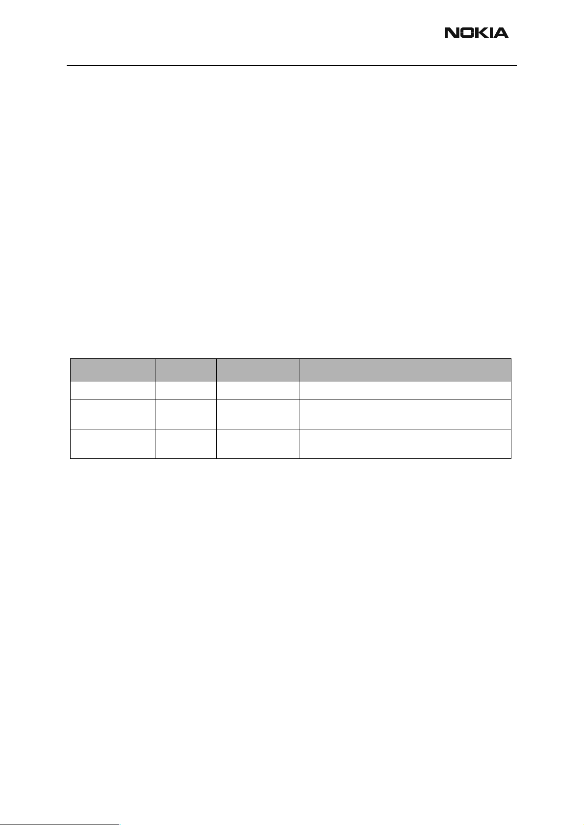
Table 1: Phone operating mode
Mode BSI-resistor BTEMP resisto r Remarks
Normal 68k 47k
Local 560_
(<1k_)
Test > 1k 560_ (<1k_) Recommended for baseband testing. Same as local
Whatever
mode, but making a phone call is possible.
If the corresponding resistors are connected, the MCU software automatically enters into
the local or test mode when the supply voltage is connected to the phone.
The power can be switched on by:
1 Pressing the power key.
2 Connecting the local/test mode resistors to the bsi/bt emp lines and connecting
the battery voltage to the phone.
3 Connecting a charger.
4 Phone’s internal functions (Real time clock alarm)
In the local and test mode, the baseband can be controlled through MBUS or FBUS (FBUS
is recommended) connections using Phoenix service software.
Troubleshooting
Note: Most of the baseband repair actions require removing the baseband shield.
The shield must not be removed unless separately authorized by the program.
Page 4 ãNokia Corporation Issue 1 10/01
Page 5

NPW-1
PAMS Technical Documentation Troubleshooting Instructions
Note: The phone’s ESN has to re-written to the UEM, if the UEM is replaced. This
can be done only in Central Service.
The BB troubleshooting instructions consist of the following topics:
1Power up
2 Flash programming
3Audio
• Earpiece
• Microphone
4 Charging
5 Accessory detection
6Sleep clock
7 User interface
Power up faults
Power up sequence
•Display
• Lights
• Buzzer
•Vibra
• Keyboard
8 Infrared
1 The UEM acts as a HW master during start up
• Vbatt limits: 2.1V for internal state machine, 3V trigger ing whole startup
• Regulator sequencing
• HW "core" regulators "on": Vio, Vcore, VR3, Vflash1
• These regulators supply the processors, memory, chip interfaces and
clock source in RF
Issue 1 10/01 ãNokia Corporation Page 5
Page 6

NPW-1
Troub l esh oot ing Instructions PAMS Technica l Do cum en tation
• Reset releasing delay
• Supply voltages stabilize to their UEM HW def ault values
• RFCLK grows to full swing
• The core is ready to run but waiting for the PURX release
• Reset releasing
• The UPP releases the SLEEPX up to the "non sleep" -state to prevent the
UEM switching the regulators "OFF"
2 MCU starts running the Bootsrap Code
• written in stone/ UPP internal ROM
• the program checks if there is any reason for the FDL mode (Flash Down
Load)
• If there is an executabl e code in FLASH and there is no r eason for FDL,
the MCU starts running the MCU program from FLASH.
3 MCU runs the FLASH MCU code
• the phone initialization, user interfaces, internal blocks etc.
• Core regulator voltage setting for required DSP speed
• Initializes the DSP and concerning HW
• Releases DSP reset -> DSP starts running
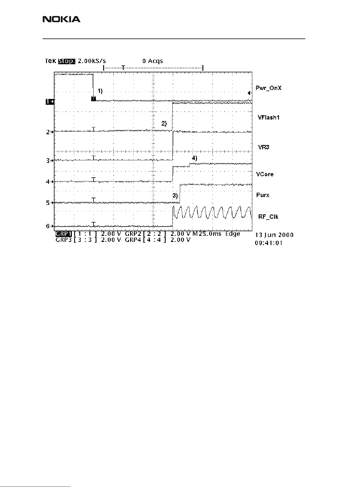
Note: In figure below, the RF_Clk frequency appears to be lower than 19.44MHz
because of a too low oscilloscope sampling frequency (2kS/s).
Page 6 ãNokia Corporation Issue 1 10/01
Page 7
NPW-1
PAMS Technical Documentation Troubleshooting Instructions
Figure 1: Power up sequence
1 Powe r key presse d
• After 20ms UEM enters RESET MODE if VBAT>Vmstr+
• VFLASH1, Vana, Vcore, Vio and VR3 goes high.
• VCTCXO enabled by VR3 -> RFClk 19.44 MHz running.
2 Purx released
• Purx released by UEM, UEMINT goes high for 100 ms, SleepX goes high and
UEM starts feeding SleepClk (32 KHz) to UPP.
Note: The sleepclock starts running in the crystal circuitry (B200) immediately when
the battery voltage is supplied.
3 Software running
• Default value for Vcore is 1.5 volts and, if the software is running, Vcore will
rise to 1.8 volts.
Issue 1 10/01 ãNokia Corporation Page 7
Page 8

NPW-1
Troub l esh oot ing Instructions PAMS Technica l Do cum en tation
• Cbus (1.08MHz) clock starts running.
Phone does not start up normally or does not stay on
Note: In case of power up faults, it is not possible to force the phone on by disabling
the watchdog. Instead, measurements should be taken immediately when the
power key is pressed or when the battery voltage is connected to the phone
(local/test mode).
The easiest way to check if the software is running when the phone takes an abnormal
amount of current is to measure the cbusclk and Vcore.
The Dbus clock (programmable 9.72MHz) is not automatically visible in the test and local
modes.
Page 8 ãNokia Corporation Issue 1 10/01
Page 9
NPW-1
PAMS Technical Documentation Troubleshooting Instructions
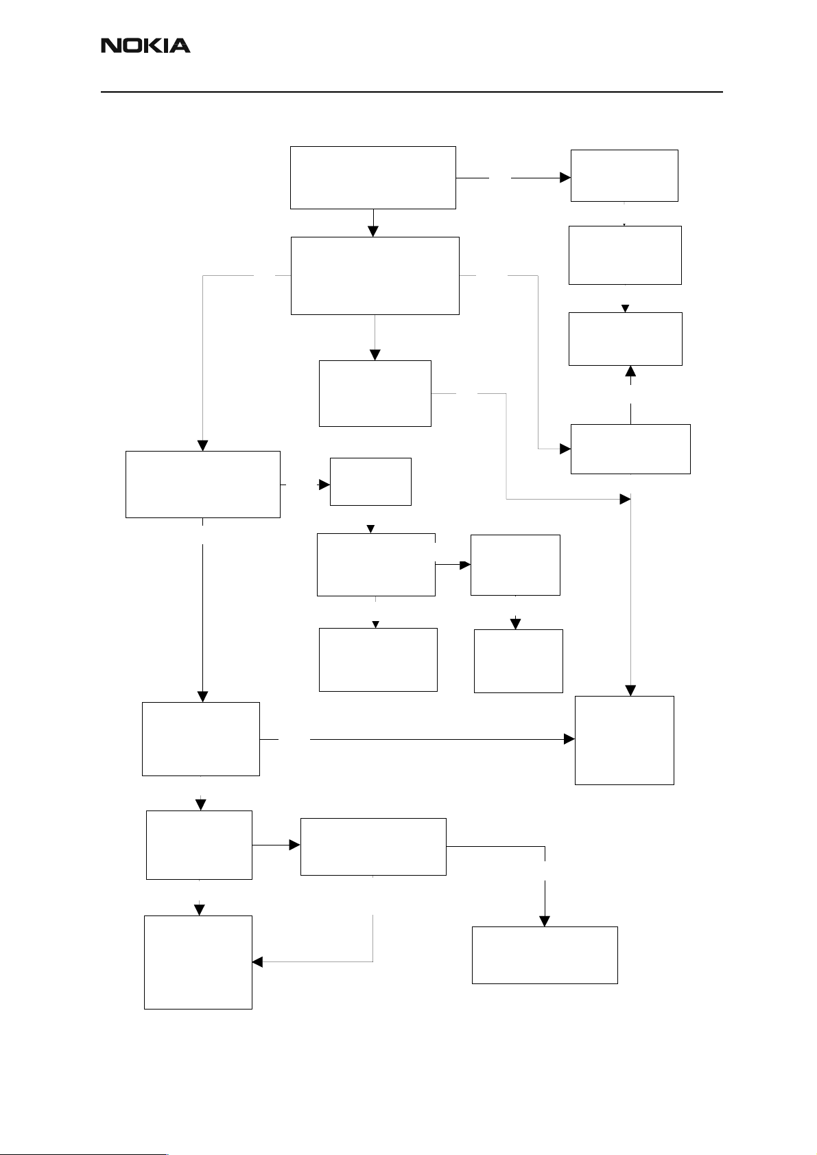
Figure 2: Fault tree, phone does not power up
OK
Check 19.44MHz
RF-clock from C420
OK
Try to start phone to
test or loc a l mode
FAIL
Measure
Vflash1,Vana,Vio,Vcore
,VR3when pwr key
pressed
VANA & VR3
missing
Check G790
(missing,
misaligned)
FAIL
Check
C420
OK
Check
19.44MHz from
G790
OK
FAIL
OK
FAIL
OK
Check
R792,C792,
C793
OK
Check the
power key
OK
Check R202,
R205, C217,
C220
OK
Check X101
FAIL
Measure VBAT
from C261
OK
Check that purx
goes up to 1.8V
OK
Measure
J406. Should
be 1.08 MHz
OK
Change UPP
(D400)
FAIL
Change N801
FAIL
Re-flash phone
Programmng ok,
but phone doesn't
start
Change
G790
Change the
UEM (D200)
Programming
fails
Go to flash failur e
chart
Issue 1 10/01 ãNokia Corporation Page 9
Page 10

NPW-1
Troub l esh oot ing Instructions PAMS Technica l Do cum en tation
Flash Programming does not work
Flash programming procedure
1 The phone communicates with the prommer via the production test pattern,
using the following signals:
• FBUSTX(serial data to phone)
• FBUSRX(serial data from phone)
• MBUS(serial clock for FBUSRX)
• VPP(External flashing voltage for speed up flashing)
• The BSI line is also used when initializing flashing (battery connector).
2 When the phone is powered (VBAT>3V), the MBUS and FBUSTX lines a re pulled
up internally by the phone.
3 The prommer sends a command to the UEM, using FBUSRX, to enter the Flash-
mode. During the sending of this co mmand, the prommer keeps the BSI line high
and MBUS is used as a serial clock.
4 When the Flash-mode command is acknowledged, UEM enters the Flash-mode
and releases reset (PURX) to MCU.
5 After reset is released, UPP checks if there is a request for the Bootstrap code
(that resides in the UPP ROM).
6 The request for Bootstrap is the MBUS pulled down by the prommer (if the boot-
strap is not requested, the bootstrap code jumps to FLASH SW).
7 If the Bootstrap code is requested, UPP enters the Flash-mode and sets FbusTX to
'0' as an acknowledgement to the prommer. This is an indication that UPP can
run, at least, the fixe d Bootstra p c ode – although it is not abl e to r un t he FLASH
code. UPP then sends an UPP-ID to the prommer via the FBUSTX line.
8 After the prommer has received the UPP-ID, it send s a corresponding Secondary
Boot Code to the phone via FBUSRX. The Secondary Boot Code, when run in UPP,
requests UPP to send information to the prommer about the flash type and other
HW-related parameters about the device to be flashed.
9 Prommer then sends the Algorithm C ode corresponding to the HW parameters,
and this algorithm, when run in UPP, takes over handling the MCUSW transfer to
Flash.
10 12 volts can be supplied to Vpp (by the prommer) to speedup flashing .
Page 10 ãNokia Corporation Issue 1 10/01
Page 11

NPW-1
PAMS Technical Documentation Troubleshooting Instructions
11 The FLASH Program includes a package of MCU and DSP software and all default
parameters for the phone. The tuning values will be adde d/rewritten during the
Flash/Alignment phase.
Flash programming error codes
The various error codes can be seen from the "FPS-8 Flash" in Phoenix.
The underlined text in the table be low means t hat t he it em unde r consider ati on is bei ng
used for the first time in the flashing sequence.
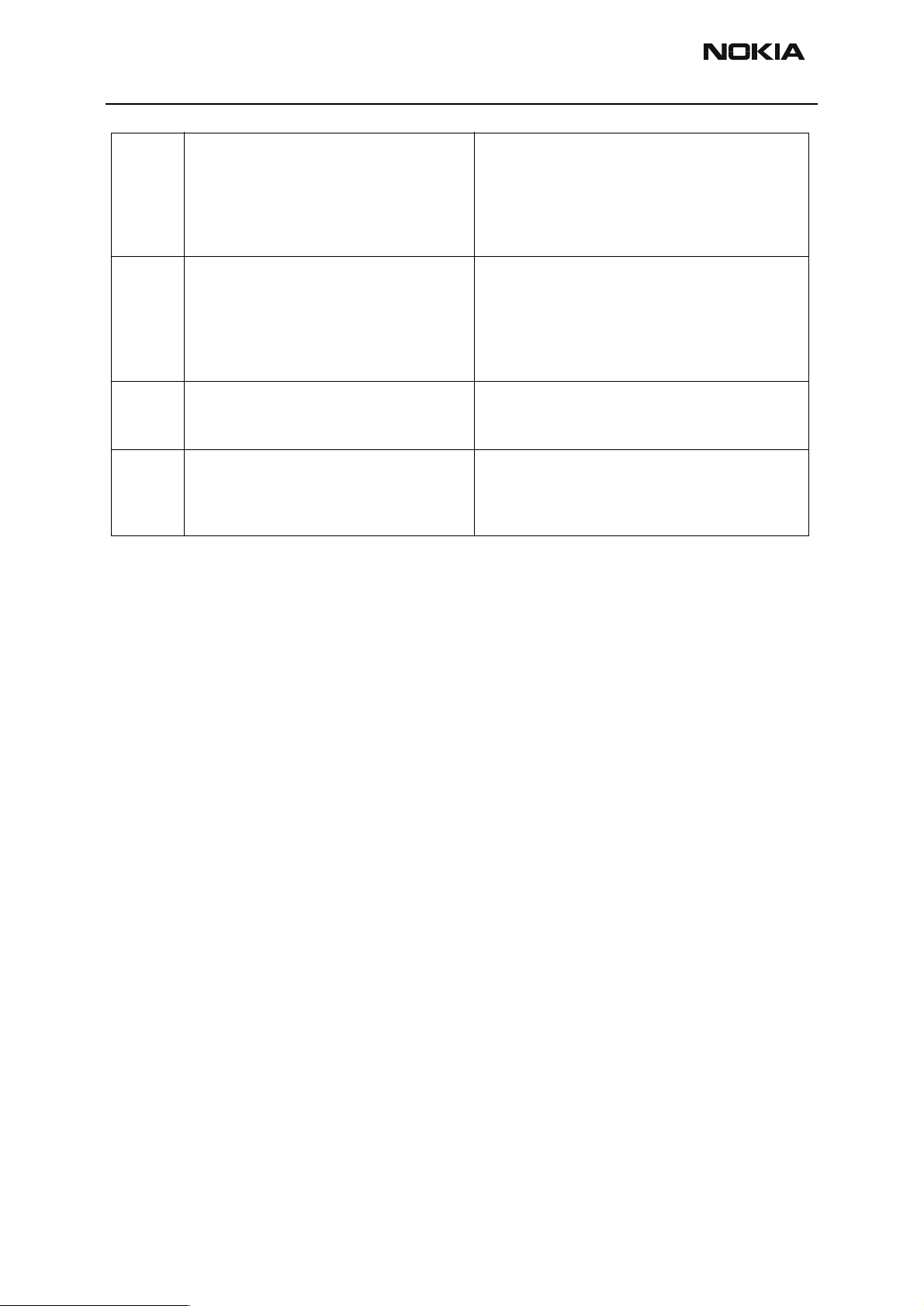
Table 2: Table 2. Flash pr ogr am min g er ror codes.
Error Description Not working properly
C101 "The Phone does not set FbusTx line high
after the startup."
C102 "The Phone does not set FbusTx line low
after the line has been high. The Prommer
generates this error also when the Phone
is not connected to the Prommer."
C103 "Boot serial line fail." Mbus from Prommer->UEM->UPP(MbusRx)(SA0)
C104 "MCU ID message sending failed in the
Phone."
C105 "The Phone has not received Secondary
boot codes length bytes correctly."
C106 "The Phone has not received Secondary
code bytes correctly."
Vbatt
Vflash1
Vcore
VIO
BSI and FbusRX from prommer to UEM.
FbusTx from UPP->UEM->Prommer(SA0)
PURX(also to Safari)
VR3
Rfclock(VCTCXO->Safari->UPP)
Mbus from Prommer->UEM->UPP(MbusRx)(SA1)
FbusTx from UPP->UEM->Prommer(SA1)
FbusRx from Prommer->UEM->UPP
FbusTx from UPP->UEM->Prommer
FbusTx from UPP->UEM->Prommer
Mbus from Prommer->UEM->UPP(MbusRx)
FbusRx from Prommer->UEM->UPP
FbusTx from UPP->UEM->Prommer
Mbus from Prommer->UEM->UPP(MbusRx)
FbusRx from Prommer->UEM->UPP
FbusTx from UPP->UEM->Prommer
C10 7 "The Phone MCU can not start Secondary
code correctly."
A204 "The flash manuf acturer and device IDs in
the existing Algorithm files do not match
with the IDs received from the target
phone."
A387 "The MC U ID in the MCUSW. ” UPP
C601 "The prommer has detected that Vpp volt-
age level has dropped below the limit"
UPP
Flash
Signals between UPP-Flash
Vpp from prommer - >Flash
Issue 1 10/01 ãNokia Corporation Page 11
Page 12
NPW-1
Troub l esh oot ing Instructions PAMS Technica l Do cum en tation
C383
C583
C683
C384
C584
C684
C585
C685
C586
C686
Charging
Note: The charging voltage and current can be checked by connecting the phone to
"The Prommer has not received Phone
acknowledge to the message."
(C383-during algorithm download to tar-
get phone)
(C583-during erasing)
(C683-during programming)
"The Phone has generated NAK signal dur-
ing data block transfer."
(C384-during algorithm download to tar-
get phone)
(C584-during erasing)
(C684-during programming)
Data block handling timeout"
(C585-during erasing)
(C685-during programming)
"The status response from the Phone
informs about fail."
(C586-during erasing)
(C686-during programming)
Flash
UPP
Signals between UPP-Flash
Flash
UPP
Signals between UPP-Flash
Flash
UPP
Signals between UPP-Flash
Flash
the service software and reading the ad- converter values of the vchar and
ichar.
If charging fails when the ACP-9 or the LCH-9 is used, and works with ACP-7, ACP-8 and
LCH-8, check that the charge control pin of the system connector is connected to the
ground.
Page 12 ãNokia Corporation Issue 1 10/01
Page 13

NPW-1
PAMS Technical Documentation Troubleshooting Instructions
Figure 3: Fault tree, charging
Phone doesn't start
charging
Connect charger and
check VCHARIN
OK
Check ICHAR
FAIL
Check
R202,R203,R205,C217,
C220,C201,C202 and
R200
OK
Change the
UEM
Fail
Check
F100,L100,V100,C105
OK
Check bottom
connector
- VIN
- Charge contr ol pi n
Audio failures
In case of audio failures, there are three possibilities to check the audio lines.
1 Make a phone call against tester and check audios.
2 In case the earpiece/XMIC fails: Feed a 1Khz signal to the XMIC line and measure
the signal from the earpiece line. T he Audio test box JBA-8 is needed. The Audio
loop (Audio test/Ext In Hp Out) must be switched on by the Phoenix service software. This loop will connect audios only through the UEM. In this case, the UPP is
not used.
In case the internal microphone/XEAR fails: Feed the tone to the microphone and
measure the signal from the XEAR line. The Audio test box JBA-8 is needed. The
Issue 1 10/01 ãNokia Corporation Page 13
Page 14

NPW-1
Troub l esh oot ing Instructions PAMS Technica l Do cum en tation
Audio loop (Audio test/Hp In Ext Out) must be switched on by the Phoenix service
software. This loop will connect audios only through the UEM. In this case, the
UPP is not used.
3 Run the audio-loop self-test with Phoenix (BB Self Tests/
ST_EAR_DATA_LOOP_TEST). This loop will test the ear-data/mic-data lines
between the UPP and the UEM.
Earpiece or external microphone line does not work
Figure 4: Fault tree, earpiece fail
Earpiece do es n 't
work
Run audio-loop
selftest with
phoenix
OK
Check R157
OK
Check
earpiece
OK
Fail
Feed 1KHz to Xmic
by JBA-8 and
measure from
earpiece
Fail
OK
Change UPP
Change UEM
Page 14 ãNokia Corporation Issue 1 10/01
Page 15

NPW-1
PAMS Technical Documentation Troubleshooting Instructions
Microphone or XEAR line does not work
Figure 5: Fault tree, microphone fail
Microphone doesn't
work
Run audio-loop
selftest with
phoenix
Ok
Check
R156,C151,C152,C157,L164
Ok
Check
microphone
Ok
Change UEM
Fail
Feed 1KHz to Mic
by JBA-8 and
measure from Xear
Fail
Ok
Chang e UPP
Accessory detection
1 Start the phone in the normal mode when checking for accessory detection.
2 The Ad- converter value of the hookint-line can be checked with the Xmic-
switch on an MJS-18 test jig. Changes normally from high to low when no accessory is connected.
3 When the headset HDC-5 is connected, the hookint- value should be between
600 and 800.
Issue 1 10/01 ãNokia Corporation Page 15
Page 16

NPW-1
Troub l esh oot ing Instructions PAMS Technica l Do cum en tation
Figure 6: Fault tree, accessory detection
Accessory detection
doesn't work normally
Check HeadInt
ad-value with Phoenix
(No acce sso ry
connected)
- He adInt ~0 *)
Fail
Check R151
and C160
Ok
Check bottom
connector
Ok
Ok
Ok
Use the xmic- switch on MJS-18
and check hookint ad-value.
Should go from high (~1000) to
low ( ~0)
Fail
Check R152,C161,L160
Ok
Check
R150,R201,C104,C105,
L162,L163
Ok
Change UEM
* On loca l or test m o d e
Headint <400
Sleep Clock
Missing/non-functional sleep clock causes
• entering sleep mode fails (higher curre nt consumption -> shorter standby time).
The
• Baseband self tests cannot be run.
• Phone clock (on display) does not function properly.
Page 16 ãNokia Corporation Issue 1 10/01
Page 17

NPW-1
PAMS Technical Documentation Troubleshooting Instructions
Figure 7: Fault tree, sleep clock
Sleep mode
not working
Measure sleep clock
from J204
Ok
Change UPP
(D400)
Fail
Measure sleep c lock
from B200
Ok
Change UEM
(D200)
Fail
Check C203
&C204
Ok
Change B200
Issue 1 10/01 ãNokia Corporation Page 17
Page 18

NPW-1
Troub l esh oot ing Instructions PAMS Technica l Do cum en tation
Display/Keyboard lights do not work
Figure 8: Fault tree, Display/Keyboard lights.
Display/Keyboard
lights are not working
Check R300 (Display) and
R301 (Keyboard)
OK
Check LEDs
V300... V303 (Display) and
V304.. . V309 (Keyboard)
OK
Use Display Test in
Phoenix to se t li ghts
ON/OFF
FAIL
FAIL
FAIL
Replace
resistor(s)
Replace
LED(s)
Replace UEM
Page 18 ãNokia Corporation Issue 1 10/01
Page 19

NPW-1
PAMS Technical Documentation Troubleshooting Instructions
Display does not work
Figure 9: Fault tree, Display does not work
Display does not work
Check that phone
powers up normally
(current consumption,
power up sequence)
OK
Check display visually
(possible cracks on
COG driver or glass,
capacitors loose or
broken
OK
Check PWB and
elastomer
connector
FAIL
FAIL
FAIL
Proceed to phone
doesn't power up
troubleshooting
Replace
display module
Clean PWB and
replace
elastomer if
needed
In any phase o f display
troublesho ot ing use Display Test i n
Phoenix to produce test patterns on
display.
Al so check with a known good
display m odule to see if it works.
OK
Run LCD test in
Phoenix
(BB Self Tests/
ST_LCD_TEST)
OK
Use Display Test
in Phoenix to
check if display
works
FAIL
Replace
display module
FAIL
Check
capacitors
C302...C304
OK
Replace
elastomer
FAIL
FAIL
display module
Replace
capacitors(s)
Replace
Issue 1 10/01 ãNokia Corporation Page 19
Page 20

NPW-1
Troub l esh oot ing Instructions PAMS Technica l Do cum en tation
Buzzer does not work
Check spring connectors and C306.
• No sound: Try using a known good buzzer instead. If there is still no sound,
change the UEM (D200)
• Weak sound: Use the Audio test in Phoenix to set the buzzer parameters (frequency, strength). If it does not effect the sound level, change the buzzer.
Vibra does not work
Check spring connectors and C307&C308.
• No vibration: Try using a known good vibra instead. If there is still no vibration,
change the UEM(D200)
• Weak vibration: Use the Vibra test in Phoenix to set the vibra’s pa rameters (frequency, duty cycle). If it does not effect the magnitude of the vibration, change
the vibra.
Keyboard does not work
Check that there is no dirt between the dome sheet and the PWB. If the keyboard still
does not operate normally, try to use the Keyboard test in Phoenix to see if the pr essed
key is identified. If it is not identified, change the UPP(D400).
Page 20 ãNokia Corporation Issue 1 10/01
Page 21

NPW-1
PAMS Technical Documentation Troubleshooting Instructions
Infrared does not work
Figure 10: Fault tree, infrared
Infra Red not working
Measure Vflash1 from IR
module VCC(pin6), should
be 2.78V
OK
Check R350, R356, C351
and V350
OK
Use
ST_IR_LOOP_TEST(in
BB Self Tests) in Phoenix
FAIL
FAIL
FAIL
OK
Change
UEM(D200)
Replace faulty
component(s)
Use
ST_IRDA_LED_TEST
(in BB Self Tests) in
Phoenix
FAIL
OK
Measure Tx Data from
IR module(pin3)
1.8V, 9.6/115.2kbps
UPP or UEM is faulty
Measure Rx Data from
OK
Change UEM
IR module(pin4)
OK
FAIL
Change IR module
Phone OK
Issue 1 10/01 ãNokia Corporation Page 21
Page 22

NPW-1
Troub l esh oot ing Instructions PAMS Technica l Do cum en tation
Receiver Troubleshooting
General instructions for RX troubleshooting
Start the Phoenix-software and use it to start the required RX-mode of the mobile
phone. The troubleshooting flowchart is divide d into three steps: (1) general checking,
(29 local checking and (3) RX- chain checking.
Always use an RF-cable connected from an external RF-connector to the analyzer via
(RF-power) attennuator. This is important to protect the analyzer against excessive RFpower and not to allow leakage of undesired RF-power into the cellular frequencies.
1 Start the Phoenix-software and select the TX mode under Testing (AMPS, DAMPS
or TDMA1900).
2 It is useful to select the mid channel (383 for AMPS/DAMPS or 1000 for
TDMA1900) and the power level 2.
Note: Before changing ASICS or Filters, all solderings and missing components must
be checked visually. After any possible component chang es, the phone must be
tuned with the Phoenix autotune SW.
Path of the received signal
Block level description of the receiver:
(Antenna/ext RF) – Diplexer – Duplexer – Low Noise Amplifier (LNA) – RX band filt er –
First mixer – 135.54 MHz RX IF filter – IF-amplifier – second mixer – 14 kHz low-pass filter – adjustable IQ amplifier – Baseband.
Fault finding charts for receiver chain
AMPS
Page 22 ãNokia Corporation Issue 1 10/01
Page 23

NPW-1
PAMS Technical Documentation Troubleshooting Instructions
Figure 11: Fault tree. AMPS
Apply 881.49 MHz =
ch 383 -116dBm ,
8kHz dev, 1 kHz sine
signal to ext er nal
RF-connect or X900.
Y
Note!
These test s are done in
local mode by using RF
Test UI.
Connect HS to cellular
tester, open audio
AF: 1 kHz sine signal,
meas SIN A D
AF: >12 dB
Check UHF Vc (from
C773) V: 1.8 ...2.1 V
Check RXVHF Vc
(from C720). V : 0.7
...1.3
N
N
Y
Y
Y
AMPS
RX-chain OK
N
Start synthesizer
troubleshooting
N
Start synthesizer
troubleshooting
Apply 881.49 MHz
-30dBm , sine s i gnal
to external
RF-connect or X900.
Issue 1 10/01 ãNokia Corporation Page 23
Page 24

NPW-1
Troub l esh oot ing Instructions PAMS Technica l Do cum en tation
Note!
Check input level
at dipl exer (Z907)
input.
Y
N
Change EXT RF
Connector
Check all soldering and components
in antenna circuit before changing
Check input level at
duplex filter. You can
also check level at
diplexer output
Y
Check input level at
LNA input (J800).
Y
Check RF level at
RX800 band filter
input.
Y
N
Change diplexer Z906
N
Change duplex filter
(Z906)
N
N
Change SAFARI
(N801)
Note!
Check all soldering and discrete
components of frontend.
Note!
Check all solderings and discrete
copmponents around SAFARI
before changing
Note!
From the begin to MIX_1A input
you should see strong RF signal
level at 881.49 MHz. Exact level
is difficult to define here because
variable impedances in RX path.
Also used probe type affects to
the results.
Check RF level at
MIX1_A input.
Y
N
Change SAFARI
(N801)
Page 24 ãNokia Corporation Issue 1 10/01
Page 25

NPW-1
PAMS Technical Documentation Troubleshooting Instructions
Check RF level at RX
IF filter input at 135.54
MHz
Y
Check RF level at RX
IF filter output at
135.54 MHz
Y
N
Check RF lev el at J751
and J752 at 2034.06
MHz
Y
Change SAFARI
(N801)
N
Change RX IF f i lter
(Z830)
N
Start synthesizer
troubleshoot
Note !
Check all discrete components and
voltages ar ound S AFARI
Check RX I and Q
signals at I: J801(+),
J803(-) and Q:
J804(+), J802(-)
Y
Check UEM and start
baseband troubles hoot
N
Check RF level by
L730 without having
electrical co nt ac t at
271.08 MHz
Change SAFARI
(N801)
N
Start synthesizer
troubleshoot
Y
Issue 1 10/01 ãNokia Corporation Page 25
Page 26

NPW-1
Note!
g
Troub l esh oot ing Instructions PAMS Technica l Do cum en tation
TDMA800
Since the same physical signal path is used for both a nalog and digital modes at the
lower band, there is no need for additional troubleshooting in the digital mode. So if the
digital mode at the lower band is not working properly, start the analog mode troubleshooting.
TDMA1900 (only dualband)
Only EXT RF connector –> 1
st
IF needs separate troubleshoot at upper band. After down
conversion (RF –> 135.54 MHz) both lower and upper band use same signal path.
Figure 12: Fault tree: TDMA1900 troubleshooting
Apply 1960.02 MH z =
ch 1000 -110 dBm
signal to external
RF-connector X900.
Y
Enable loop back BER
using RF Test UI and
check sensitivity: -110
dBm BER < 3%
N
N
Check UHF Vc (from
C773) V: 2. 2 . ..2.6 V
Y
Y
N
N
TDMA1900
RX-chain is OK
Start synthesizer
troubleshooting
These tests are done
in local mode by usin
RF Test UI.
Check RXVHF Vc
(from C720). V: 0.7
...1.3
Y
Start synthesizer
troubleshooting
Page 26 ãNokia Corporation Issue 1 10/01
Page 27

NPW-1
s
PAMS Technical Documentation Troubleshooting Instructions
Note!
Check input level
of diplexer (Z907)
Y
Check input level of
duplex filter (Z962)
Y
Check RF level at LNA
input (at duplex filter
RX output port)
Y
N
Change EXT RF
Connec tor
N
Change diplexer
(Z907)
N
Change duplex filter
(Z962)
N
Check all soldering and component
in antenna circuit before changing
Note!
Check all soldering and discrete
components of frontend.
Note!
Before replacing S A FA R I check
all the solderings and components
around V850
Check RF level at
RX1900 band filter
(Z850) input
Y
N
Check voltage at C854
out (V850 in). V: about
2.7V
Change SAF A RI
(N801)
Issue 1 10/01 ãNokia Corporation Page 27
Page 28

NPW-1
Troub l esh oot ing Instructions PAMS Technica l Do cum en tation
Y
N
Check RF level at
MIX1_B input
Y
Check RF level at RX
IF filter input at 135.54
MHz
Y
Continue
troubleshooting like LB
Change RX1900
bandfilter
N
Check RF level at J 751
and J752 at
2095.56MHz
Y
Change SAFARI
(N801)
N
Start s y nthesizer
troubleshoot
Note !
Check all discrete components and
voltages around of SAFARI
Transmitter Troubleshooting
General instructions for TX troubleshooting
Always use an RF-cable connect ed from an ex ternal RF-connector to the analyzer via (rfpower) attennuator. This is important to protect the analyzer against excessive RF-power
and not to allow leakage of undesired RF-power into the cellular frequencies.
1 Start the Phoenix-software and select the TX mode under Testing (AMPS, DAMPS
or TDMA1900).
2 It is useful to select the mid channel (383 for AMPS/DAMPS or 1000 for
TDMA1900) and the power level 2.
Note: After any component change, tune the phone with the Phoenix autotune SW.
Path of the transmitted signal
AMPS/DAMPS
UEM TX I/Q DA-converters -> I/Q modulator and Digital gain step ampl ifier (SAFARI) ->
IF-BPF -> Upconverter+ drive r -> B P F -> PA -> Coupler (Power detector) -> Duplex-filter
-> Diplexer -> EXT RF-connector -> Antenna
l
Page 28 ãNokia Corporation Issue 1 10/01
Page 29

NPW-1
PAMS Technical Documentation Troubleshooting Instructions
TDMA1900 (ONLY DUALBAND)
UEM TX I/Q DA-converters -> I/Q modulator and Digital gain step ampl ifier (SAFARI) ->
IF-BPF -> Upconverter + driver (SAFARI) ->Balun -> BPF -> PA->Coupler (Power detector) -> Duplex-filter -> Diplexer -> EXT RF-connector -> Antenna
The power detection and power control circuit belongs under the power control part of
this guide.
Fault finding charts for the transmitter
AMPS
1 Start the Phoenix-software and set the phone to the Analog mode by using RF
Test UI.
2 Set the channel to 383 and the power level to 2.
3 Connect the RF-cable to the Ext RF co nnector.
4 Connect the cable to the Spectrum analyzer input.
5 Measure the RF level.
Note: Insertion loss of the cable and attenuations.
Issue 1 10/01 ãNokia Corporation Page 29
Page 30

NPW-1
Troub l esh oot ing Instructions PAMS Technica l Do cum en tation
Figure 13: Fault tree. Transmitter troubleshooting
AMPS, PL2, CH383
Visual check of TX
block
- PA and up converter
-TX SAW
- Duplex filter
- Passive components
OK
Check LO-signal
(1017.03 MHz)@up
converter
and TX VHF (361.08
MHz)@N750
OK
Check supply voltage
- VR2
- VBATTRF
- VR5
- IPA1
- TXP1
OK
Check TXi/q signals
Test points J901...J904
OK
NOK
NOK
NOK
Start synth
troubleshooting
Check UEM and UPP
(Baseband)
Check UEM
(Baseband)
Check TX IF input
power (180.54 MHz) @
up converter
IF: -20 dBm +3 /-6 dB
OK
Check TX RF (836.49
MHz) output power and
@ up converter
RF: 0 dBm +/- 6dB
OK
NOK
Change SAFARI
NOK
Change up converter
Page 30 ãNokia Corporation Issue 1 10/01
Page 31

NPW-1
PAMS Technical Documentation Troubleshooting Instructions
Check TX S AW
input and output
power
IL: -3 dB
OK
Is Itot 700...800 mA?
Check PA output power
and gain.
Output power: ~28
dBm
Gain: ~30 dB
OK
Check PWRDET N930
insertion loss
IL< 0.3 dB
NOK
Change TX SAW filter
Z905
NOK
Change P A N901
NOK
Change PWRDET
N930
OK
Check duplexer Z906 ,
diplexer Z907 and RF
connector X900
insertion loss
Dupl IL ~2. 2 dB
Dipl ~0.35 dB
RF conn ~0.1 dB
OK
Star t P ower control
troubleshooting
TDMA800
NOK
Change Z906 or Z907
or RF connector
The transmitter chain is exactly the same as the AMPS-mode, except for the IPA current,
and thus it is important that the AMPS have no faults.
Issue 1 10/01 ãNokia Corporation Page 31
Page 32

NPW-1
Troub l esh oot ing Instructions PAMS Technica l Do cum en tation
TDMA1900 (only dualband)
TDMA1900 mode and DAMPS mode have a common RF modulator and thus it is important that the DAMPS mode have no faults.
Figure 14: TDMA1900 troubleshooting
TDMA 1900, PL2, CH1000
NOK
Is TDMA800 mode
OK?
OK
Start AMPS
troubleshooting
Check LO-signal
(2079.78 MHz)@T775
and TX VHF (363.6
MHz)@N750
OK
Check supply voltage
- VR2
- VBATTRF
- VR6
- IPA2
- TXP2
OK
Check TX IF input
power (181.80 MHz) @
Z960
IF: -20 dBm +3 /-6 dB
OK
Check TX RF
(1879.98.MHz) output
power @T960 input
RF: 0 dBm +/- 6dB
NOK
NOK
NOK
NOK
Start synth
troubleshooting
Check UEM and UPP
(Baseband)
Change SAFARI or
Z960
Change SAFARI
OK
Check Z961 input and
output power
IL: -3dB
OK
NOK
Change Z961
Page 32 ãNokia Corporation Issue 1 10/01
Page 33

NPW-1
PAMS Technical Documentation Troubleshooting Instructions
Is Itot 350...450 mA?
Check PA output power
and gain.
Output power: ~29
dBm
Gain: ~30 dB
OK
Check P WRDET N930
insertion loss
IL< 0.3 dB
OK
Check duplexer Z62 ,
diplexer Z907 and RF
connector X900
insertion loss
Dupl IL ~2.2 dB
Dipl ~0.35 dB
RF conn ~0.1 dB
NOK
Change P A N960
NOK
Change PWRDET
N930
NOK
Change Z906 or Z907
or RF connector
OK
Star t Power control
troubleshooting
Po wer control loop
Basically, the power detection is done with the Power detector module a nd power con-
trol is done inside the SAFARI. Power detection is similar for both bands, except that
both bands have their own coupler.
Issue 1 10/01 ãNokia Corporation Page 33
Page 34

NPW-1
t
Troub l esh oot ing Instructions PAMS Technica l Do cum en tation
Figure 15: Fault tree: Power control loop
Note !
See PWRDET vs. Outpu
power curve
Is PWRDET vs.
output power OK?
See chart below.
N
Check VR2 and
RFTEMP .
Check C930, C931
and PWRDET
module.
Y
N
Is DAC value vs.
PWRDET (mV) OK?
Check UEM
(BaseBand)
The detected voltages are illustrated in the following table and diagram:
Table 3: Typical detected voltages at power levels PL2...PL10 (DB)
800A 800D 1900D
Pout TXPWRDET Pout TXPWRDET Pout TXPWRDET
PL dBm dac mV dBm dac Mv dBm dac mV
2 26.5 633 1671 27.3 696 1839 27.3 662 1746
3 22.5 393 1038 23.3 433 1142 23.3 405 1069
4 18.5 237 625 19.3 261 688 19.3 245 648
5 14.5 141 372 15.3 155 410 15.3 147 387
6 10.5 82 215 11.3 90 237 11.3 84 222
7 6.5 46 120 7.3 50 132 7.3 46 122
8 - - - 3.3 27 70 3.3 24 64
9 - - - -0.7 13 33 -0.7 11 30
§0----4.75 12 -4.75 12
Note: DAC values may vary about +- 20%
Note: TXPWRDET is the difference between TX on burst and off burst.
Page 34 ãNokia Corporation Issue 1 10/01
Page 35

NPW-1
PAMS Technical Documentation Troubleshooting Instructions
Figure 16: Detected voltage levels
2000
1800
1600
1400
1200
1000
800
600
Detected voltage [mV]
400
200
0
246810
Synthesizer Troubleshooting
There are four oscillators generating the needed f requencies for RF-section. 19. 44 MHz
reference oscillator, 2GHz UHF VCO, TX VHF cascade amplifier VCO and RX VHF VCO integrated in Safari. RX VHF frequency is fixed 271.08 MHz and TX VHF has two fixed frequencies, 361.08 MHz for lowband and 363.6 MHz for upper band. VCO's operating
frequencies are controlled by PLL-circuit of SAFARI. All locals are locked to stable
19.44MHz reference oscillator.
800A
800D
1900D
Power level
The frequency range for 2GHz UHF VCO is: 2009.1 … 2125.53 MHz. The output frequency
range for the lower band is from 2009.1 to 2059.02MHz. In upper band the output frequency range from the UHF VCO is from 2031.81MHz to 2125.53MHz.
It is practical way to check out synthesizer status by measuring control voltage of the
VCO from Integrator capacitor. If voltage is stable and reasonable, local oscillators are
running correctly.
19.44 MHz reference oscillator
The 19.44 MHz oscillator frequency (G790) is controlled by UEM. This 19.44 MHz signal
is connected to SAFARI an d there in PLL-circuits and from SAFARI to UPP.
All synthesizers use divided VCTCXO signal as a reference signal for Phase locked loop to
provide correct LO-frequency.
Baseband also needs a reference signal where it can generate necessary the clock signals
and the VCTCXO output signal is also buffered and connected to the UPP.
Issue 1 10/01 ãNokia Corporation Page 35
Page 36

NPW-1
Troub l esh oot ing Instructions PAMS Technica l Do cum en tation
Fault finding chart for 19.44 MHz oscillator
Figure 17: Fault tree: 19.44 MHz oscillator
2
Change
VCTCXO
OK
2.No
START HERE!
Is VCTCXO
oscillating?
19.44MHz
C792
2.78 V
No
R792
OK
1
OK
1.No
Check voltage
Check resistor
OK!
RX VHF VCO
The RX VHF VCO signal is used to generate receiver Intermediate frequency. RX VHF VCO
has one fixed frequency 271.08 MHz. Operating frequency is locked in Phase locked Loop.
RX VHF VCO output signal is fed to SAFARI. Inside the SAFARI signal is divided for Phase
detector and RX parts. Before I/Q-modulator freq uency is divided by 2.
Fault finding chart for RX VHF VCO
Measure oscillator frequency over L730 coil. Don´t connect the probe to the pads!
AMPS, CH383
Page 36 ãNokia Corporation Issue 1 10/01
Page 37

NPW-1
PAMS Technical Documentation Troubleshooting Instructions
Figure 18: Fault tree: RX VHF VCO
4
Change
SAFARI
3
Check loopifilter
components:
C720, R721, C721, R722,
C722, R733, C733
check also R724
OK
3.No
No
START HERE
Is oscillator locked
to 271.08 MHz
L730 and DC blo ck C726
OK
1
2.No
Check r esonator
V725, C724, C725,
OK
2
components:
Yes
OK!
TX VHF VCO
The TX VHF VCO signal is used to generate transmitter Intermediate f requency. TX VHF
VCO has two fixed frequencies 361.08 MHz for lower band and 363.6 MHz for upper
band. Operating frequency is loc ked in Phase locked Loop and frequency is divided by
two before modulator.
Fault finding chart for TX VHF VCO
AMPS, CH383 -> TX VHF frequency 361.08 MHz
TDMA1900, CH1000 -> TX VHF frequency 363.6 MHz
Issue 1 10/01 ãNokia Corporation Page 37
Page 38

NPW-1
Troub l esh oot ing Instructions PAMS Technica l Do cum en tation
Figure 19: Fault tree: TX VHF VCO
4
Check components:
C740, C741, C742, R741,
R742, R743 and
C749, C750, L750
3
Check resonator
components:
V744, C745, L746,
C747, C748
4.No
OK
3.No
Change
cascade amplifier
OK
Is osc illator locked
5.No
1
START HERE
to 361.08 MHz
or 363.6 MHz
2.No OK
Check operating
voltage:
4.75 V
at R745
5
N750
2
OK
6.No
Yes
No
OK
OK
6
Change
SAFARI
OK!
Check:
L751, R745
UHF SYNTHESIZER
The UHF synthesizer consists of a e xt ernal 2GH z UHF VCO, loop filter and int egrate d PLL
in Safari RF-IC. Safari T IC contains stages like counters, pre-scaler, divider by two, phase
and frequency comparator and a charge pump circuit which allows two operational
modes analog and digital. The UHF VCO Oscillation frequency is from 2009.1MHz to
2125.53
In upper band (TDMA1900) 2 GHz synthesizer frequency is fed straight to mixers. In the
lower band case (AMPS & TDMA800), 2 GHZ UHF VCO frequency signals are first divided
by 2 inside SAFARI and then that divided signal is fed to the mixers. The output frequency of the VCO depends on the DC-control voltage, which is controlled by the P LLcircuit inside the SAFARI.
Page 38 ãNokia Corporation Issue 1 10/01
Page 39

NPW-1
PAMS Technical Documentation Troubleshooting Instructions
Fault finding chart for UHF SYNTHESIZER
Figure 20: Fault tree: UHF Synthesizer
Change
VCO
2. No
OK
Check
loopfilter
components
and balun
OK
3.
No
START HERE!
Is frequency locked?
2009.1 - 2125.53
MHz
1.
OK
No
Check VCO
operatig
voltage:
2.78 V
Yes
No
OK
4. No
Is EVM OK?
No
1
Check loopfiler
components
Check resistor
R774
OK
Change
No
YES
SAFARI
low
band
Low band:
Is divided
signal OK?
OK!
Yes
No
Issue 1 10/01 ãNokia Corporation Page 39
Page 40

NPW-1
Troub l esh oot ing Instructions PAMS Technica l Do cum en tation
Page 40 ãNokia Corporation Issue 1 10/01
 Loading...