

Page 1

Nokia Customer Care
RH-37 Series Transceivers
6(b) - RF Troubleshooting
Instructions
Issue 1 07/04 2004 Nokia Corporation Page 1
Company Confidential
Page 2

RH-37
6(b) - RF Troubleshooting Instructions Nokia Customer Care
[This page left intentionally blank]
Page 2 Nokia Corporation Issue 1 07/04
Page 3

RH-37
Nokia Customer Care 6(b) - RF Troubleshooting Instructions
Table of Contents
Page No
General Information on RF Troubleshooting.................................................................................... 5
Test environment ..................................................................................................................................5
Test conditions ......................................................................................................................................6
Receiver Verification and Troubleshooting ...................................................................................... 7
General instructions for RX troubleshooting ................................................................................7
Measuring RX I/Q signals using RSSI reading ..............................................................................7
Measuring RX performance using SNR measurement ............................................................ 9
Measuring front-end power levels using spectrum analyzer............................................. 10
Measuring analogue RX I/Q signals using oscilloscope....................................................... 11
Fault finding chart of the receiver ................................................................................................12
Transmitter ............................................................................................................................................. 19
General instructions for TX troubleshooting ..............................................................................19
GSM900 transmitter ..........................................................................................................................19
General instructions for GSM TX troubleshooting ................................................................ 19
Fault finding chart for GSM900 transmitter .......................................................................... 22
GSM1800 transmitter .......................................................................................................................24
General instructions for GSM1800 TX troubleshooting ...................................................... 24
Fault finding chart for GSM1800 transmitter........................................................................ 26
GSM1900 transmitter .......................................................................................................................28
General instructions for GSM1900 TX troubleshooting ...................................................... 28
Fault finding chart for GSM1900 transmitter........................................................................ 30
Synthesizer ............................................................................................................................................. 33
General instructions for synthesizer troubleshooting ..............................................................33
Checking synthesizer operation .....................................................................................................33
Fault finding chart for PLL synthesizer ........................................................................................36
Frequency tables .................................................................................................................................38
GSM900 (including EGSM900)................................................................................................... 38
GSM1800 .......................................................................................................................................... 39
GSM1900 .......................................................................................................................................... 41
DC Supply Voltage Check ................................................................................................................... 43
Appendix 6A: Test Points..................................................................................................... 45
Receiver test points ...........................................................................................................................47
Transmitter test points ......................................................................................................................49
Synthesizer test points ......................................................................................................................52
Issue 1 07/04 Nokia Corporation Page 1
Page 4

RH-37
6(b) - RF Troubleshooting Instructions Nokia Customer Care
[This page left intentionally blank]
Page 2 Nokia Corporation Issue 1 07/04
Page 5

RH-37
Nokia Customer Care 6(b) - RF Troubleshooting Instructions
General Information on RF Troubleshooting
Notes:
Several bills of material (BOM): There are two different kinds of VCOs, VCTXOs, RF-PAs, SAW-filters and Antenna Switches (ASM) assembled. They may only be replaced with the same type as the
original component (from the same manufacturer).
Phoenix version: In this document there are example measurements being depicted with pictures of
AMS-Phoenix, version A 2004.06.1.69. In later versions pictures of menus and windows may look differently.
Layout version: The drawings of test points and component placement in this version of the document
are taken from build B4.0 layout (1cna_41). If you use the document for newer layout versions, make
sure to use the corresponding assembly and test point drawings.
Test environment
It is assumed, that the phones are disassembled and tested with a repair jig MJ-22R.
The following measurements have to be done for repairing the phone boards:
• RF measurements shall be done using a spectrum analyzer together with a highfrequency probe. Note that the signal will be significantly attenuated. Correct
attenuation can be checked using a “good” phone board for example.
• LF (low frequency) and DC measurements shall be carried out with an oscillo-
scope together with a 10:1 probe.
•For receiver measurements, a signal generator specified for frequencies up to
2000 MHz is required. The signal generator is connected to the antenna port of
the repair jig.
Most of the radio communication testers, like CMU200, can be used as a signal
generator, but make sure to have a continuous (CW) signal without modulation
for alignment purposes.
• Transmitter output level measurements shall be done with a power meter
which is connected to the antenna port of the repair jig.
Always make sure that the measurement set-up is calibrated when measuring RF parameters at the antenna port. Remember to put the correct losses of the module repair jig
and the connecting cable in Phoenix or in the set-up programs of the RF generators
when realigning the phone.
Apart from key-components described in this document, there are a lot of discrete components (resistors, inductors and capacitors) for which troubleshooting has to be done by
checking its proper soldering and complete assembly on the PWB. Capacitors and resistors can be checked by means of an ohm-meter, but be aware in-circuit measurements
should be evaluated carefully.
Issue 1 07/04 Nokia Corporation Page 5
Page 6

RH-37
6(b) - RF Troubleshooting Instructions Nokia Customer Care
Test conditions
Rx tuning of the 26 MHz reference oscillator (VCTCXO) is temperature sensitive
because of the estimations of <AFC_value> and <AFC_slope>. According to the Production Test Specification DCS02294-EN-0.5, the ambient temperature has to be within a
temperature range of 22°C to 28°C.
Most RF semiconductors are static discharge sensitive. ESD protection must be taken
into account during repair (ground straps and ESD soldering irons).
The RF ASIC Helgo is moisture sensitive. Therefore, the ASIC must be pre-baked prior
to soldering.
Page 6 Nokia Corporation Issue 1 07/04
Page 7

RH-37
Nokia Customer Care 6(b) - RF Troubleshooting Instructions
Receiver Verification and Troubleshooting
General instructions for RX troubleshooting
Connect the phone to a PC, which has Phoenix Service Software and a dongle installed,
using either
• repair jig and DAU-9S (RS232) cable or
• repair jig and XCS-4 cable via FPS-8 Flash Box or
• DAU-9T cable (RS232).
Connect the phone to a power supply (DC voltage: 3.6V, max. current: 3A) and an RF signal generator. Switch the phone on.
Start Phoenix Service Software and open FBUS connection.
Select Scan Product Ctrl-R
and wait until the phone information (RH-37) is shown in the lower right corner of the
screen.
Follow the instructions below.
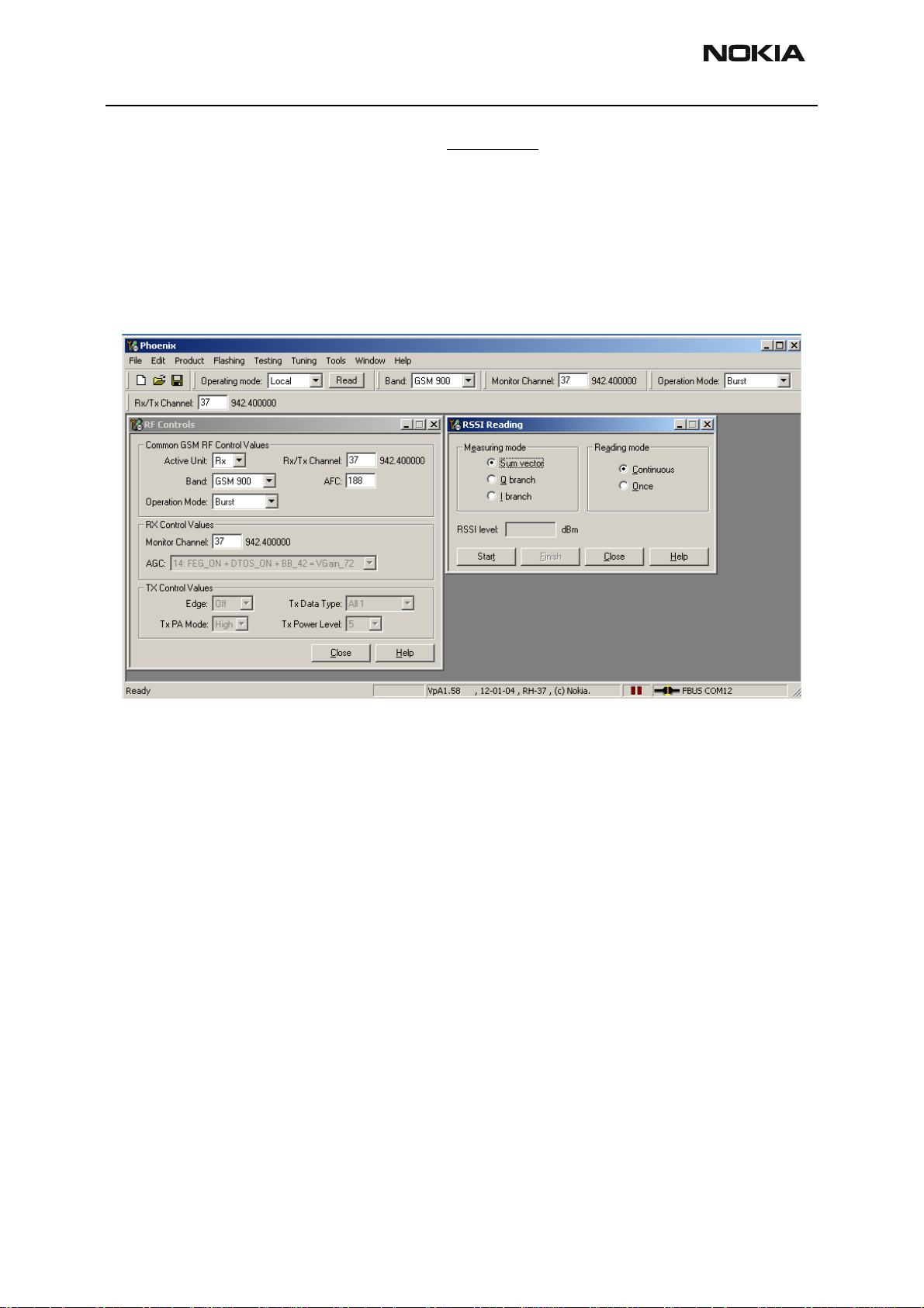
Measuring RX I/Q signals using RSSI reading
Start Phoenix Service Software and open FBUS connection.
Select Scan Product Ctrl-R
Wait until the phone information is shown in the lower right corner of the screen.
Set the operating mode to local mode
Select Testing T
RF Controls F
Select Band GSM 900 or GSM1800 or GSM1900
Active unit RX
Operation mode Burst
RX/TX Channel 37 or 700 or 661
Select Testing T
Issue 1 07/04 Nokia Corporation Page 7
Page 8
RH-37
6(b) - RF Troubleshooting Instructions Nokia Customer Care
RSSI reading R
In the RSSI Reading window, the <measuring mode> shall be set on Sum vector and the
<reading mode> on Continuous.
The set up should now look like this:
(The example below shows a screen shot in GSM900!)
Make the following settings on your signal generator:
Frequencies:
• GSM 900: 942.46771 MHz (channel 37+ 67.710 kHz offset)
• GSM 1800: 842.86771 MHz (channel 700 + 67.710 kHz offset)
• GSM 1900: 1960.06771 MHz (channel 661+ 67.710 kHz offset)
RF power level:
• – 80 dBm @ the antenna connector of the phone/ test jig
(remembering to compensate for the cable and jig attenuation).
Click on <Read now> in RSSI reading.
The resulting RSSI level shall be – 80 dBm +/– 0.5 dB in each band.
Page 8 Nokia Corporation Issue 1 07/04
Page 9

RH-37
Nokia Customer Care 6(b) - RF Troubleshooting Instructions
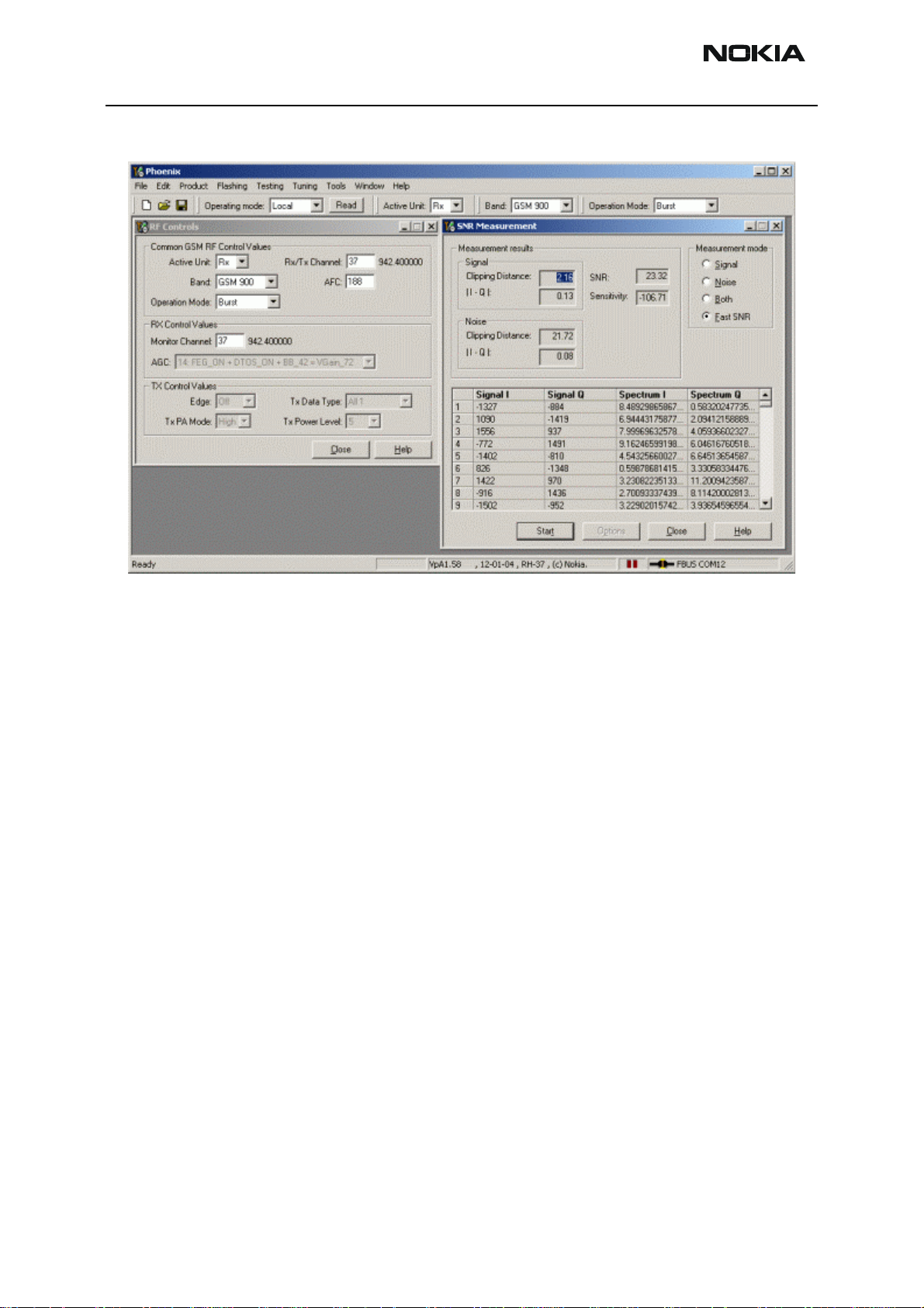
Measuring RX performance using SNR measurement
Start Phoenix Service Software and open FBUS connection.
Select Scan Product Ctrl-R
Wait until the phone information is shown in the lower right corner of the screen.
Set operating mode to <local mode>.
Select Testing T
RF Controls F
Select Band GSM 900 or GSM1800 or GSM1900
Active unit RX
Operation mode Burst
RX/TX Channel 37 or 700 or 661
Select Testing T
SNR Measurement M
Select Measuring mode Fast SNR (Radio Button)
Press Start
The window <Signal Measurement> pops up informing on frequency and power level of
the signal generator to be set. Follow the command <Turn ON the RF generator>.
Press <ok> and the window will close.
Read the SNR result from the window SNR Measurement. The value shall exceed:
• GSM 900: > 20 dB
• GSM 1800: > 18 dB
• GSM 1900: > 18 dB
The set up should now look like this:
Issue 1 07/04 Nokia Corporation Page 9
Page 10
RH-37
6(b) - RF Troubleshooting Instructions Nokia Customer Care
(The example below shows a screen shot in GSM900!)
Choose the remaining GSM bands and measure accordingly the procedure described
above.
Measuring front-end power levels using spectrum analyzer
Spectrum analyzer (SA) level values depend on the probe type and shall be verified by a
properly working phone sample. The levels that are given in this document are measured
with a resistive probe (50 Ohm semi-rigid cable).
Start Phoenix Service Software and open FBUS connection.
Select Scan Product Ctrl-R
Wait until the phone information is shown in the lower right corner of the screen.
Set <operating mode> to <local mode>.
Select Testing T
RF Controls F
Select Band GSM 900 or GSM1800 or GSM1900
Active unit RX
Operation mode Continuous
Page 10 Nokia Corporation Issue 1 07/04
Page 11

RH-37
Nokia Customer Care 6(b) - RF Troubleshooting Instructions
RX/TX Channel 37 or 700 or 661
Please refer to the fault finding chart and Appendix for proper levels at different test
points.
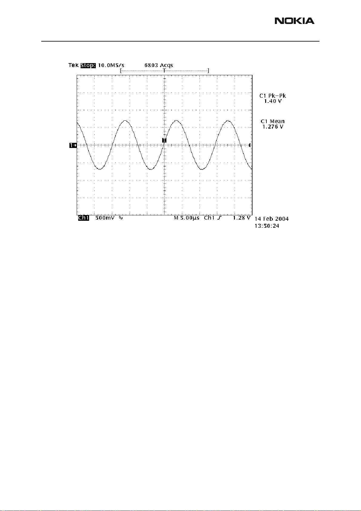
Measuring analogue RX I/Q signals using oscilloscope
Measuring with an oscilloscope RX I and RX Q signals on the test points <RXI> respectively <RXQ> is recommended only if the RSSI reading does not provide enough information. Input level = -60dBm.
Start Phoenix Service Software and open FBUS connection.
Select Scan Product Ctrl-R
Wait until phone information is shown in the lower right corner of the screen.
Set operating mode to <local mode>.
Select Testing T
RF Controls F
Wait until the RF Controls window pops up.
Select Band GSM 900 or GSM1800 or GSM1900
Active unit RX
Operation mode continuous
RX/TX Channel 37 or 700 or 661
AGC 10
The following picture should be displayed on an oscilloscope's screen if the receiver is
working properly:
Issue 1 07/04 Nokia Corporation Page 11
Page 12
RH-37
6(b) - RF Troubleshooting Instructions Nokia Customer Care
Signal amplitude 1.40Vpp
DC offset ≈ 1.28V as the offset is floating, switch to the operating mode
<Burst> in Phoenix and read the DC offset
Frequency 67kHz
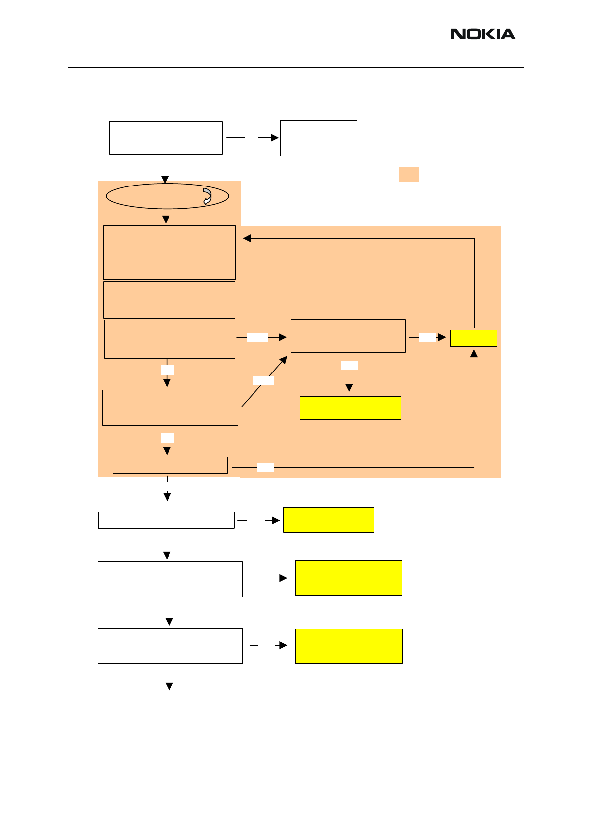
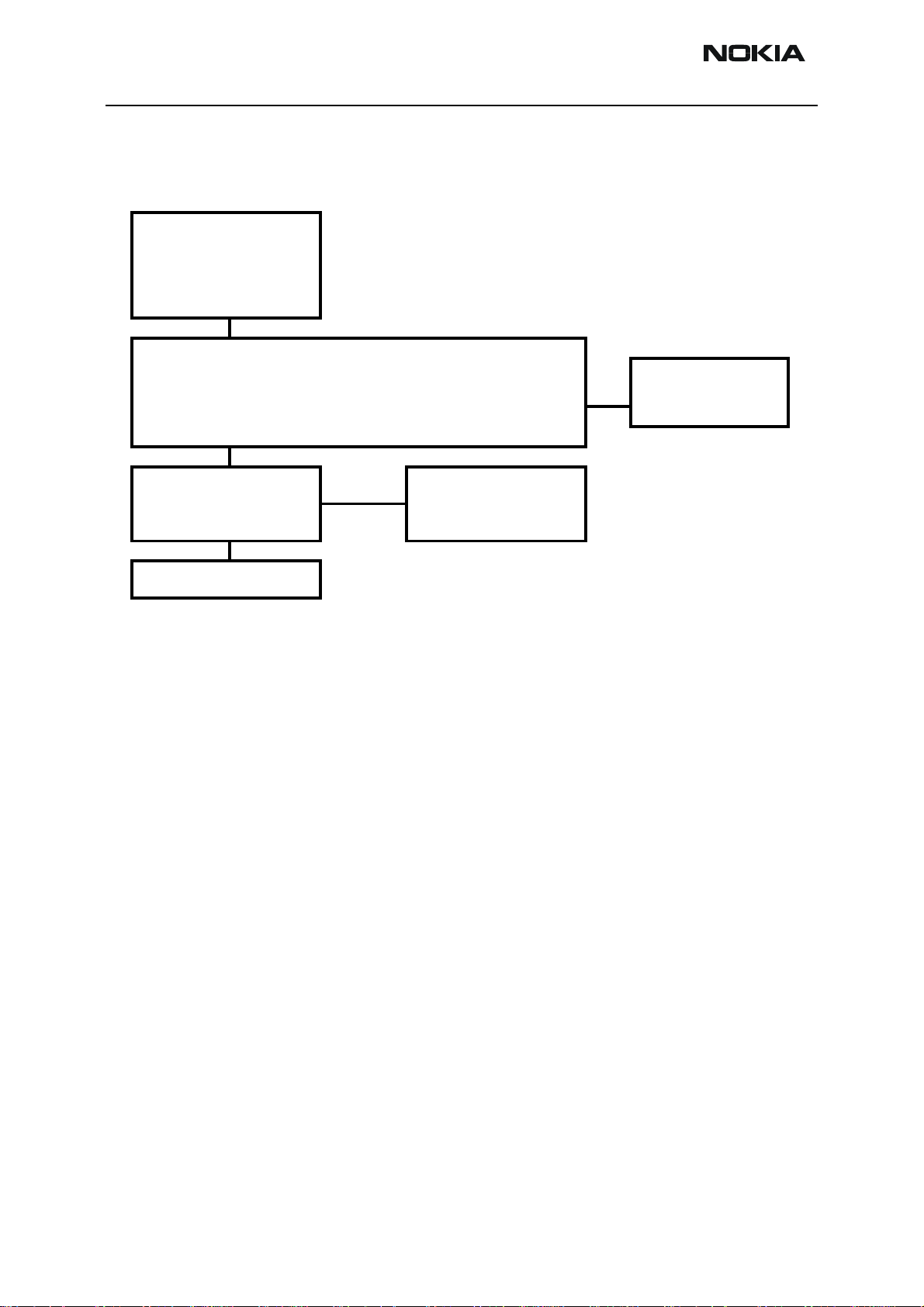
Fault finding chart of the receiver
During fault finding, the calibration procedure is used to find out, whether all bands are
affected (error in common part of the Rx chain) or only one band (error in a Rx part of
the failed band). Take care not to save calibration values to the phone memory,
which are out of limits. Find the error first and repair it.
When a defective phone has been calibrated, a possible error in RX front-end might be
masked. In that case, one can get a reasonable RSSI reading, although the front-end
shows excessive losses. If it is not sure that incorrect re-calibration has been made, following steps shall be carried out:
• Check if AGC calibration is within limits.
• Check if SNR reading is o.k.
Use an oscilloscope to check levels of “RXI” and “RXQ”.
The RF ASIC generates only single ended I and Q signals (RXI, RXQ). As the A/D converter
in UEM requires two differential signals, an artificial mid voltage is generated from
Page 12 Nokia Corporation Issue 1 07/04
Page 13
RH-37
Nokia Customer Care 6(b) - RF Troubleshooting Instructions
VrefRF02. The phone layout has dedicated test points for the analogue RX I and Q signals
(J512, J513).
The BB part is used to measure those signals by means of RSSI reading. This works only if
correct calibration has been carried out in production.
RSSIreading [dBm] = 20log(UBB/U
LSB
) - AGC
calibrated
In order to check the levels and frequencies of RF signals, the following probe can be
used (note that only the core lead contacts the test point, the shielding of the coaxial
cable does not contact GND during the measurement):
Connect this probe via a coaxial cable and a DC block to a spectrum analyzer. The DC
block is important to protect the spectrum analyzer from DC levels, which superpose
the RF signal at several test points.
If both RX and TX path seem to be faulty, it has to be checked if the synthesizer is working.
Issue 1 07/04 Nokia Corporation Page 13
Page 14
RH-37
A
A
A
6(b) - RF Troubleshooting Instructions Nokia Customer Care
Phoenix:
Phone: local mode
Open
Signal Generator:
Phoenix:
Open
Check RSSI Level = -80dBm
Execute Rx Calibration in selected
band, refer to chapter 9.2.1
re calibration results within limits?
Make sure that
Synthesizer is working
Yes
All 3 bands
RF Controls
Active Unit: Rx
Op. Mode: Burst
Rx/Tx channel: default (mid)
Level: –80dBm
Frequency: calculated from
Phoenix + 67.71kHz
RSSI reading
No
:
see
No
Yes next bandNo
Synthesizer Fault
Finding Tree
Yes
Selected band is working and
calibrated.
re all 3 bands measured?
Yes
Rx chain is functional
and calibrated
Receiver
Fault Finding Tree
part 1
= To be done in all
three bands.
No
re all 3 bands measured?
Yes
Are all 3 bands defective?
Yes
Oscilloscope:
Check supply voltages of RF ASIC:
VR4 = 2.8V ? (TP: VR4)
Yes
Oscilloscope:
Check supply voltages of RF ASIC:
VR6 = 2.8V ? (TP:VR6)
Yes
No
No
Continue with single
band fault finding.
No
No
Check supply filter
components (C2233,
C7519, C7520) and UEM
Check supply filter
components (C2231,
C7521) and UEM
Receiver
Fault Finding Tree
part 2
Receiver
Fault Finding Tree
part 3
Page 14 Nokia Corporation Issue 1 07/04
Page 15
RH-37
r
Nokia Customer Care 6(b) - RF Troubleshooting Instructions
Oscilloscope:
Check reference voltages of RF part:
VrefRF01 = 1.35V ?
(TP: VrefRF01*)
Yes
No
Check supply filter
components (R7511,
C7524) and UEM
Receiver
Fault Finding Tree
part 4
Oscilloscope:
Check reference voltages of RF part:
VrefRF02 = 1.35V ?
(TPs: VrefRF02* and VrefRF02**)
Yes
Phoenix:
Phone: local mode
RF Controls
Active Unit: Rx
Op. Mode:
Rx/Tx channel: default (mid)
AGC: 14
:
Continuous
Signal Generator:
To be tuned that input power at spectrum
analyzer: –60dBm
(power at probe:
Frequency: calculated from Phoenix
offset: 67.71kHz
= approx. -63 dBm)
Pref
Spectrum Analyzer: 1)
Check Rx/Tx Switch (Diplexer)
Depending on selected band, check level at TPs:
GSM900 output Rx1 Pref -1.5dB ?
GSM1800 output Rx2 Pref -2.0dB ?
GSM1900 output Rx3 Pref -2.5dB
Yes
Check supply filter
No
components (R2900,
R2901, C2900, C2901)
and UEM
Receive
Fault Finding Tree
part 5
No
?
Change Z7800
Note 1):
RF levels are dependent on RF probe and have to be validated
with a known good sample.
Oscilloscope:
RX IQ levels ok (TPs: RXI, RXQ) ?
Yes
Oscilloscope:
RF-BB serial interface ok?
(TPs: RFBusData, RFBusClk, RFBusEna1)
No
No
Yes
Change RF
ASIC (Helgo)
BB error:
Check UPP
Change RF
ASIC (Helgo)
Receiver
Fault Finding Tree
part 6
Issue 1 07/04 Nokia Corporation Page 15
Page 16
RH-37
6(b) - RF Troubleshooting Instructions Nokia Customer Care
Select faulty band in Phoenix and continue measurements on dedicated Rx part.
Phoenix:
SNR Measurement
open
Meas. Mode: Fast SNR
Measure
Press
Signal Generator:
Level: –92dBm
Frequency: calculated from Phoenix
Phoenix:
SNR measurement ok?
(SNR > 18.37dB)?
Phoenix:
Phone: local mode
RF Controls
Active Unit: Rx
Op. Mode:
Rx/Tx channel: default (mid)
AGC: 14
.
No
:
Continuous
Single band fault finding
Yes
Front end is ok.
Phoenix:
Phone: local mode
RF Controls
Active Unit: Rx
Op. Mode:
Rx/Tx channel: default (mid)
AGC: 10
Signal Generator:
Level: –60dBm
Frequency: calculated from Phoenix
offset: 67.71kHz
Continue with Rx Fault Finding part 6.
:
Continuous
Receiver
Fault Finding Tree
part 7
Receiver
Fault Finding Tree
part 8
Signal Generator:
To be tuned that input power at spectrum
analyser: –60dBm
power at probe:
Frequency: calculated from Phoenix
offset: 67.71kHz
=approx. -63dBm)
Pref
Spectrum Analyzer: 1)
Center Freq: calculated from Phoenix
RBW 20kHz
Check Rx SAW filter and matching
network of selected band:
GSM900 TPs: INM_G_RX / INP_G_RX
both output levels > Pref -3.5dB ?
GSM1800 TPs: INM_D_RX / INP_D_RX
both output levels > Pref -6dB ?
Yes
No
Note 1):
RF levels are dependent on RF probe and have to be validated
with a known good sample.
Change Rx SAW filters (Z7802,
Z7803) or component(s) of
matching network depending on
selected band
Page 16 Nokia Corporation Issue 1 07/04
Page 17

RH-37
g
1)
Nokia Customer Care 6(b) - RF Troubleshooting Instructions
If selected band = GSM1900
Spectrum Analyzer:
Check SAW filter Z7801:
TP: OUT-Z7801
Output signal > Pref - 3.5dB
No
Spectrum Analyzer:
Check external LNA V7800:
TP: OUT-V7800
Output signal > Pref +14dB
Spectrum Analyzer:
Check balun T7800 and matching network:
TPs: INM_P_RX / INP_P_RX
Both output signals > Pref +12dB
RF ASIC N7500 seems to be
defective. Exchange N7500.
Yes
Yes
Yes
Yes
No
Yes
1)
No
1)
Oscilloscope:
Check voltages for V7800:
No
Voltage at C7802 = 2.5V ?
e at C7800 = 0V ?
Volta
Receiver
Fault Finding Tree
part 9
Change Z7801
Check supply
No
around V7800
filter components
and RF ASIC
Yes
No
Note 1):
RF levels are dependent on RF probe and have to be validated
with a known good sample.
Change T7800
Issue 1 07/04 Nokia Corporation Page 17
Page 18

RH-37
6(b) - RF Troubleshooting Instructions Nokia Customer Care
Make sure that Synthesizer is
working and supply voltages of
RF ASIC are ok
Phoenix:
Phone: local mode
RF Controls
Active Unit: Rx
Op. Mode:
Rx/Tx channel: default (mid)
AGC: 14
Signal Generator:
Level: –60dBm
Frequency: 942.4MHz
Offset: 67.71kHz
:
Burst
Continue measurement only when channel select filter calibration failed
Channel select filter fault finding
Receiver
Fault Finding Tree
part 10
Oscilloscope:
RF-BB filter signals ok?
TPs: CM_F_Q & CM_F_I
CM_DTOS_Q & CM_DTOS_I
Yes
Repair finished
No
Re-solder capacitor array C7523
Re-calibrate
Channel Select Filter
Calibration ok ?
NoYes
Change RF
ASIC (Helgo)
Make following tunings/calibrations
Tx power l evel tuning
x
Tx IQ tuning
x
x Rx calibration
Rx Band Filter Response Calib.
x
Page 18 Nokia Corporation Issue 1 07/04
Page 19

RH-37
Nokia Customer Care 6(b) - RF Troubleshooting Instructions
Transmitter
General instructions for TX troubleshooting
Connect the phone to a PC, which has Phoenix Service Software and a dongle installed,
using either
• repair jig and DAU-9S (RS232) cable or
• repair jig and XCS-4 cable via FPS-8 Flash Box or
• DAU-9T cable (RS232)
Connect the phone to a power supply (DC voltage of 3.6V) and switch the phone on. The
value of the DC voltage of 3.6V at the phone battery connector is crucial.
Connect an RF cable between the test jig and the measurement equipment (GSM test
equipment, power meter, spectrum analyzer, or similar).
Make use of an adequate attenuator at the input of your measurement equipment (10dB
to 20dB are recommended for a spectrum analyzer or a power meter). Additionally, a DC
block is recommended. Assure not to overload or destroy the equipment.
It is strongly recommended to use TXP as external trigger for all TX tunings. External triggering gives the following advantages:
• trigger for spectrum analyzer (gated sweep)
• trigger for oscilloscope
• trigger for power meter (avoid exchanging of attenuator and getting better accuracy in power measurements)
Start Phoenix Service Software and open FBUS connection:
Select Scan Product Ctrl-R
and wait until the phone information is shown in the lower right corner of the screen.
Follow the instructions in the chapters below.
GSM900 transmitter
The GSM900 chapters apply only for RH-37 (EU variant).
General instructions for GSM TX troubleshooting
Start the preparations as described in chapter “General instructions for TX troubleshooting”.
Issue 1 07/04 Nokia Corporation Page 19
Page 20

RH-37
6(b) - RF Troubleshooting Instructions Nokia Customer Care
GMSK
Set operating mode to local mode.
Select Testing RF Controls
Wait until the RF Controls window pops up
Select Band GSM 900
Active unit TX
Operation mode Burst
RX/TX Channel 37
TX Power Level 10
TX Data Type Random
Edge Off
The setup should now look like this:
Now the measurement equipment should detect the following output signal of the
phone:
Page 20 Nokia Corporation Issue 1 07/04
Page 21

RH-37
Nokia Customer Care 6(b) - RF Troubleshooting Instructions
P
= +23dBm @ 897.4 MHz
out
If this is not the case, go to the GMSK fault finding chart for the GSM900 transmitter.
EDGE
Set operating mode to local mode.
Select Testing RF Controls
Wait until the RF Controls window pops up.
Select Band GSM 900
Active unit TX
Operation mode Burst
RX/TX Channel 37
TX Power Level 10
TX Data Type All1
Edge On
The setup should now look like this:
Issue 1 07/04 Nokia Corporation Page 21
Page 22

RH-37
6(b) - RF Troubleshooting Instructions Nokia Customer Care
Now the measurement equipment should detect the following output signal of the
phone:
P
= +24.5 dBm @ 897.4 MHz
out
If this is not the case, go to the EDGE fault finding chart for GSM900 transmitter.
Fault finding chart for GSM900 transmitter
In the following, it is assumed that the TXP signal is used as trigger signal. For that, a
TXP test point is provided.
Page 22 Nokia Corporation Issue 1 07/04
Page 23

RH-37
Nokia Customer Care 6(b) - RF Troubleshooting Instructions
GMSK
Use Phoenix to select
TX_Data Type: Random
TX Power Level: 10
Ch37
Ensure Vbatt=3.6 V
Yes
Oscilloscope
C7711
R7511
C7512
TXP testpoint
C7517
R7516
Yes
Oscilloscope
C7529
C7529
C7530
C7530
Yes
Oscilloscope
C7701
VC1
VC2
VC3
R7713
Yes
Spectrum analyzer No Check
Z7700 out, R7704 in RFin_850/
Compare with good
Yes Synthesizer
Mode
VREF01
VR2
TXP
VR5
VR3
TXIOUTP
Vdc = 1.35 Volt Check
Vdc = 2.78 Volt No Baseband
V = 1.8 Volt
Vdc = 2.78 Volt
Vdc = 2.78 Volt
V = 0 Volt
67kHz
No Check
Vac = 0.45 Vpp, Vdc =
1.2 V
TXIOUTN
67kHz
Baseband
Vac = 0.45 Vpp, Vdc =
1.2 V
TXQOUTP
67kHz
Vac = 0.45 Vpp, Vdc =
1.2 V
TXQOUTN
67kHz
Vac = 0.45 Vpp, Vdc =
1.2 V
VTXB_900
CONT1
CONT2
CONT3
VPCTRL_90
0
V = 2.78 Volt No Check:
V = 0 Volt Helgo Serial Interface
V = 0 Volt Helgo
V = 2.7 Volt
V = 1.17 Volt
P>= 2 dBm, 897.4MHz EGSM TX SAW Filter
900
Helgo
sample
Spectrum analyzer Check PA N7700
Z7800 TX1 (PA N7700
RFOut_850/900)
Power = +24.3 dBm,
No Check Power Loop
(TXC, Vpctrl900, DET)
897.4 MHz
Yes
Spectrum analyzer Check
RF@Test-Jig No
Pout
Antenna Switch (Z7800)
= +23 dBm, 897.4 MHz
Yes
GSM900 TX
OK
Issue 1 07/04 Nokia Corporation Page 23
Page 24

RH-37
6(b) - RF Troubleshooting Instructions Nokia Customer Care
EDGE
Ensure that GMSK is ok.
Use Phoenix to select
TX_Data Type: All 1
EDGE: On
TX Power Level: 10
Ch37
Ensure Vbatt=3.6 V
Yes
Oscilloscope
C7702
C7711
VPCTRL_900
Yes
Spectrum analyzer Check PA N7700
RF@Test-Jig No Check Power Loop
Pout
= +24.5 dBm, 897.4MHz
Yes
GSM900 TX
OK
IREF01
Mode
R7713
(TXC,Rfin 900, DET)
V ~ 1.77 Volt Check
V = 1.8 Volt No Baseband
V= 2.7 V
GSM1800 transmitter
General instructions for GSM1800 TX troubleshooting
Start the preparations as described in chapter “General instructions for TX troubleshooting”.
GMSK
Set operating mode to local mode.
Select Testing RF Controls
Wait until the RF Controls window pops up
Select Band GSM 1800
Active unit TX
Operation mode Burst
RX/TX Channel 700
TX Power Level 5
TX Data Type Random
Edge Off
Page 24 Nokia Corporation Issue 1 07/04
Page 25

RH-37
Nokia Customer Care 6(b) - RF Troubleshooting Instructions
The setup should now look like this:
EDGE
Now the measurement equipment should detect the following output signal of the
phone:
P
= +23dBm @ 1747.8 MHz
out
If this is not the case, then go to the GMSK fault finding chart for GSM1800 transmitter.
Set operating mode to local mode.
Select Testing RF Controls
Wait until the RF controls window pops up.
Select Band GSM 1800
Active unit TX
Operation mode Burst
RX/TX Channel 700
TX Power Level 5
Issue 1 07/04 Nokia Corporation Page 25
Page 26

RH-37
6(b) - RF Troubleshooting Instructions Nokia Customer Care
TX Data Type All 1
Edge On
The setup should now look like this:
Now the measurement equipment should detect the following output signal of the
phone:
P
= +21.5 dBm @ 1747.8 MHz
out
If this is not the case, then go to the EDGE fault finding chart for GSM1800 transmitter.
Fault finding chart for GSM1800 transmitter
In the following, it is assumed that the TXP signal is used as trigger signal. For that, a
TXP test point is provided.
Page 26 Nokia Corporation Issue 1 07/04
Page 27

RH-37
Nokia Customer Care 6(b) - RF Troubleshooting Instructions
GMSK
TX_Data Type: Random
TX Power Level: 5
Ch700
Ensure Vbatt=3.6 V
Yes
Oscilloscope
C7711
R7511
C7512
TXP testpoint
C7517
R7516
Yes
Oscilloscope
C7529
C7529
C7530
C7530
Yes
Oscilloscope
C7709
VC1
VC2
VC3
R7715
Yes
Spectrum analyzer No Check
T7700 out, R7709 in RFin_180
Compare with good
Yes Synthesizer
Spectrum analyzer Check PA N7700
Z7800 TX2 (PA N7700
RFOut_1800/1900)
Power = +21.6 dBm,
1747.8 MHz
Yes
Spectrum analyzer Check
RF@Test-Jig No
Pout
= +20 dBm, 1747.8 MHz
Yes
GSM 1800 TX
OK
Mode
VREF01
VR2
TXP
VR5
VR3
TXIOUTP
Vdc = 1.35 Volt Check
Vdc = 2.78 Volt No Baseband
V = 1.8 Volt
Vdc = 2.78 Volt
Vdc = 2.78 Volt
Vac = 0.4 Vpp, Vdc =
V = 0 Volt
No Check
1.2 V
TXIOUTN
Vac = 0.4 Vpp, Vdc =
Baseband
1.2 V
TXQOUTP
Vac = 0.4 Vpp, Vdc =
1.2 V
TXQOUTN
Vac = 0.4 Vpp, Vdc =
1.2 V
VTXB_1800
_1900
CONT1
CONT2
CONT3
VPCTRL_18
00_1900
V = 2.7 Volt No Check
V = 2.7 Volt Helgo Serial Interface
V = 2.7 Volt Helgo
V = 0 Volt
V > 1.14 Volt
P> 2 dBm, 1747.8MHz T7700 Balun
0/1900
Helgo
sample
No Check Power Loop
(TXC, Vpctrl 1800 1900,
DET)
Antenna Switch (Z7800)
Issue 1 07/04 Nokia Corporation Page 27
Page 28
RH-37
6(b) - RF Troubleshooting Instructions Nokia Customer Care
EDGE
Ensure that GMSK is ok.
Use Phoenix to select
TX_Data Type: All 1
EDGE: On
TX Power Level: 5
Ch700
Ensure Vbatt=3.6 V
Yes
Oscilloscope
C7702
C7711
VPCTRL_900
Yes
Spectrum analyzer Check PA N7700
RF@Test-Jig No Check Power Loop
Pout
= +21.5 dBm, 1747.8
MHz
Yes
GSM 1800 TX
OK
IREF_900
Mode
R7715
(TXC, RFin 1800 1900,
V = 1.83 Volt Check
V = 1.8 Volt No Baseband
Vdc= 2.7 V
DET)
GSM1900 transmitter
General instructions for GSM1900 TX troubleshooting
Start the preparations as described in chapter “General instructions for TX troubleshooting”.
GMSK
Set operating mode to local mode.
Select Testing RF Controls
Wait until the RF Controls window pops up.
Select Band GSM 1900
Active unit TX
Operation mode Burst
RX/TX Channel 661
TX Power Level 5
TX Data Type Random
Edge Off
Page 28 Nokia Corporation Issue 1 07/04
Page 29

RH-37
Nokia Customer Care 6(b) - RF Troubleshooting Instructions
The setup should now look like this:
EDGE
Now the measurement equipment should detect the following output signal of the
phone:
P
= +23dBm @ 1880 MHz
out
If this is not the case, then go to the GMSK fault finding chart for GSM1900 transmitter.
Set operating mode to local mode.
Select Testing RF Controls
Wait until the RF Controls window pops up.
Select Band GSM 1900
Active unit TX
Operation mode Burst
RX/TX Channel 661
TX Power Level 5
TX Data Type All1
Issue 1 07/04 Nokia Corporation Page 29
Page 30

RH-37
6(b) - RF Troubleshooting Instructions Nokia Customer Care
Edge On
The setup should now look like this:
Now the measurement equipment should detect the following output signal of the
phone:
= +21.5 dBm @ 1880 MHz
P
out
If this is not the case, then go to the EDGE fault finding chart for GSM1900 transmitter.
Fault finding chart for GSM1900 transmitter
In the following, it is assumed that the TXP signal is used as trigger signal. For that, a
TXP test point is provided.
Page 30 Nokia Corporation Issue 1 07/04
Page 31

RH-37
Nokia Customer Care 6(b) - RF Troubleshooting Instructions
GMSK
Use Phoenix to select
TX_Data Type: Random
TX Power Level: 5
Ch661
Ensure Vbatt=3.6 V
Yes
Oscilloscope
C7711
R7511
C7512
TXP testpoint
C7517
R7516
Yes
Oscilloscope
C7529
C7529
C7530
C7530
Yes
Oscilloscope
C7709
VC1
VC2
VC3
R7715
Yes
Spectrum analyzer No Check
T7700 out, R7709 in RFin_180
Compare with good
Yes Synthesizer
Spectrum analyzer Check PA N7700
Z7800 TX2 (PA N7700
RFOut_1800/1900)
Power = +21.6 dBm, 1880
MHz
Yes
Spectrum analyzer Check
RF@Test-Jig No
Pout
= +20 dBm, 1880 MHz
Yes
GSM 1900 TX
OK
Mode
VREF01
VR2
TXP
VR5
VR3
TXIOUTP
Vdc = 1.35 Volt Check
Vdc = 2.78 Volt No Baseband
V = 1.8 Volt
Vdc = 2.78 Volt
Vdc = 2.78 Volt
Vac = 0.4 Vpp, Vdc =
Vdc = 0 Volt
No Check
1.2 V
TXIOUTN
Vac = 0.4 Vpp, Vdc =
Baseband
1.2 V
TXQOUTP
Vac = 0.4 Vpp, Vdc =
1.2 V
TXQOUTN
Vac = 0.4 Vpp, Vdc =
1.2 V
VTXB_1800
_1900
CONT1
CONT2
CONT3
VPCTRL_18
00_1900
V = 2.78 Volt No Check
V = 2.7 Volt Helgo Serial Interface
V = 2.7 Volt Helgo
V = 0 Volt
V = 1.12 Volt
P> 2 dBm, 1880 MHz T7700 Balun
0/1900
Helgo
sample
No Check Power Loop
(TXC Vpctrl 1800 1900,
DET)
Antenna Switch (Z7800)
Issue 1 07/04 Nokia Corporation Page 31
Page 32
RH-37
6(b) - RF Troubleshooting Instructions Nokia Customer Care
EDGE
Ensure that GMSK is ok.
Use Phoenix to select
TX_Data Type: All 1
EDGE: On
TX Power Level: 5
Ch661
Ensure Vbatt=3.6 V
Yes
Oscilloscope
C7702
C7711
VPCTRL_1800 1900
Yes
Spectrum analyzer Check PA N7700
RF@Test-Jig No Check Power Loop
Pout
= +21.5 dBm, 1880 MHz
Yes
GSM 1900 TX
OK
IREF_900
Mode
R7715
(TXC, RFin 1800 1900,
V = 1.83 Volt Check
V = 2.78 Volt No Baseband
V= 2.7 V
DET)
Page 32 Nokia Corporation Issue 1 07/04
Page 33

RH-37
Nokia Customer Care 6(b) - RF Troubleshooting Instructions
Synthesizer
General instructions for synthesizer troubleshooting
Connect the phone to a PC, which has Phoenix Service Software and a dongle installed,
using either
• repair jig and DAU-9S (RS232) cable or
• repair jig and XCS-4 cable via FPS-8 Flash Box or
• DAU-9T cable (RS232).
Connect the phone to a power supply (DC voltage of 3.6V) and switch the phone on.
Follow the instructions in the chapters below.
Checking synthesizer operation
Start Phoenix Service Software and open FBUS connection.
Select “Scan Product” (Ctrl-R or in menu File - Scan Product).
Wait until phone information is shown in the lower right corner of the screen.
Set <operating mode> to <Local>.
Open window “RF Controls” (menu Testing - RF Controls)
Set the synthesizer to the following mode:
Select Band GSM 1800
Active unit RX
Operation mode Continuous
RX/TX Channel 700
Issue 1 07/04 Nokia Corporation Page 33
Page 34

RH-37
6(b) - RF Troubleshooting Instructions Nokia Customer Care
The setup should now look like this:
The VCO chamber has a fixed shielding lid, which can only be opened by destroying it. To
enable measurements with a closed lid, holes are located at positions where the supply
voltage VR7, the tuning voltage Vc and the output frequency f
Figure 1: Test holes in the VCO chamber
Tuning voltage
Vc @ C7503
Output frequency
f
@ R7503
VCO
VCO supply voltage
VR7 @ C7500
can be measured.
VCO
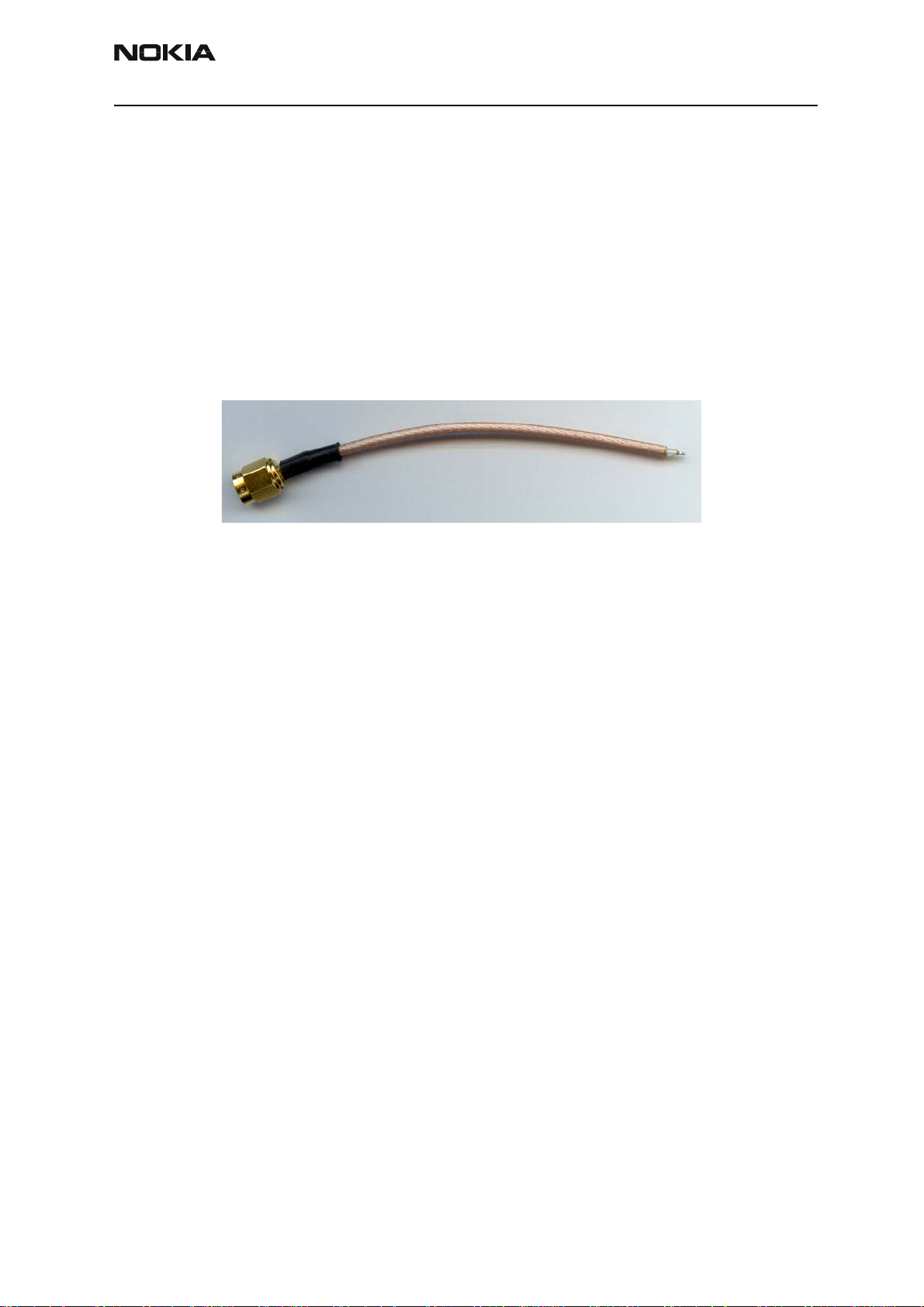
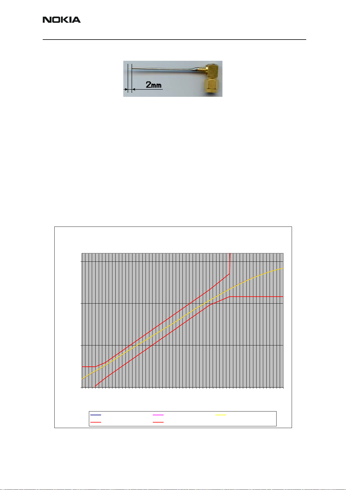
The VCO frequency has to be measured with a special probe, which fits into the holes of
the shielding lid. A thin coax cable can be used for this purpose, where the outer conductor is removed for 2mm. The isolation and the inner conductor must fit into the hole of
the shielding lid and provide a capacitive coupling to the attenuator R7503 at the VCO
output. A spectrum analyzer is used to display the frequency.
Page 34 Nokia Corporation Issue 1 07/04
Page 35
RH-37
Nokia Customer Care 6(b) - RF Troubleshooting Instructions
Figure 2: VCO probe
The VCO frequency is twice the Rx frequency in the GSM1800 band:
f
= 2 * fRX = 2 * 1842.8 MHz = 3685.6 MHz
VCO
The tuning voltage can be easily measured at the Vc input of the VCO. The corresponding
hole in the shielding lid enables the voltage measurement at C7503, which shows the
same DC voltage as Vc.
The tuning voltage should be 2.1VDC .. 2.6VDC at f
= 3685.6MHz.
VCO
The tuning sensitivity of the VCO is typically 250MHz/V. The typical relation of VCO frequency and tuning voltage is shown in the following diagram:
Figure 3: Typical frequency tuning curve for the FDK VCO
Temperature: +25°C
4500
4000
Frequency [MHz]
3500
3000
00.511.522.533.544.555.56
VCTRL [V]
2.55V @ 24.4 .. 25.4°C 2.7V @ 24.4 .. 25.4°C 2.85V @ 24.4 .. 25.4°C
High limit Low limit
Issue 1 07/04 Nokia Corporation Page 35
Page 36

RH-37
A
6(b) - RF Troubleshooting Instructions Nokia Customer Care
Even if the PLL is not working properly (Vc outside the valid range), a frequency at the
output of the VCO can be detected between 3GHz and 4.4 GHz (if the VCO itself is ok and
the supply voltage VR7 = 2.78V is applied).
If the frequency or the tuning voltage have other values than given above, see the fault
finding chart for PLL syntesizer below.
Fault finding chart for PLL synthesizer
Figure 4: PLL Fault Finding Tree
Phoenix:
Phone is responding to Phoenix commands. For example,
Ctrl-R reads the right phone information.
No
Yes
Baseband part is not working,
possible reason: 26MHz missing.
Oscilloscope
VCTCXO output at G7501
26MHz,app.0.8Vpp
No
Oscilloscope:
Check VCTCXO supply
(VR3=2.78V, this can be checked after
power on for a time of about
fter that time the voltage is going
down.)
Yes
Oscilloscope
REFCLK output of N7500:
Signal VCTCXO=RFCLK_I
at C2902, R2902.
26MHz,app.0.8Vpp
.
32sec
Yes
No
Yes
No
Synthesizer
Fault Finding Tree
part 1
Check Baseband part for errors
Check supply filter components:
R7519, C7522, VDIG at N7500
Check C2902, R2902 and N7500.
Check UEM and Software.
VCTCXO G7501 defective or
short circuit to GND.
Check supply filter components :
C2235, R7516, C7526.
Check UEM and base band part.
Page 36 Nokia Corporation Issue 1 07/04
Page 37

RH-37
Nokia Customer Care 6(b) - RF Troubleshooting Instructions
Setup with Phoenix:
Band: GSM 1800
Mode: RX Continuous
Channel: 700
Spectrum analyzer
VCO out (G7500)
f
= 3685.6 MHz
VCO
Vc of VCO = 2.1..2.6V
No
Spectrum analyzer
VCO out (G7500)
Some signal 3 - 4.4 GHz
Yes
Oscilloscope
VCO tuning voltage
Vc of VCO = 0V
Yes
Oscilloscope
VCO supply
(VR7 = 2.78V)
PLL Block is functional
No
Yes
No
Synthesizer
Fault Finding Tree
part 2
Check R7503 and T7500.
Change VCO G7500
Check supply filter components:
C2203, R7500, C7500, C7501
Check UEM.
Yes
Oscilloscope
PLL supply
(VR1=4.7V, VR5=2.78V)
No
Oscilloscope
Check RFBus signals
RFBusClk, RFBusData,
RFBusEn1 ok?
Yes
No
Yes
No
Change RF ASIC N7500
Check baseband part.
Check loop filter components:
C7502, C7503, C7504, R7501, R7502
Short circuit to ground?
RF ASIC N7500 could be defective.
Check supply filter components:
C2232, C299, C7516, C7517, C7518
Check UEM.
It is important to note that the power supply VR3 of the VCTCXO is only switched off in
the so called ‘Deep Sleep Mode’ and the power supply VR7 of the VCO (G7500) is
switched off in so called ‘Sleep Mode’.
Issue 1 07/04 Nokia Corporation Page 37
Page 38

RH-37
6(b) - RF Troubleshooting Instructions Nokia Customer Care
Frequency tables
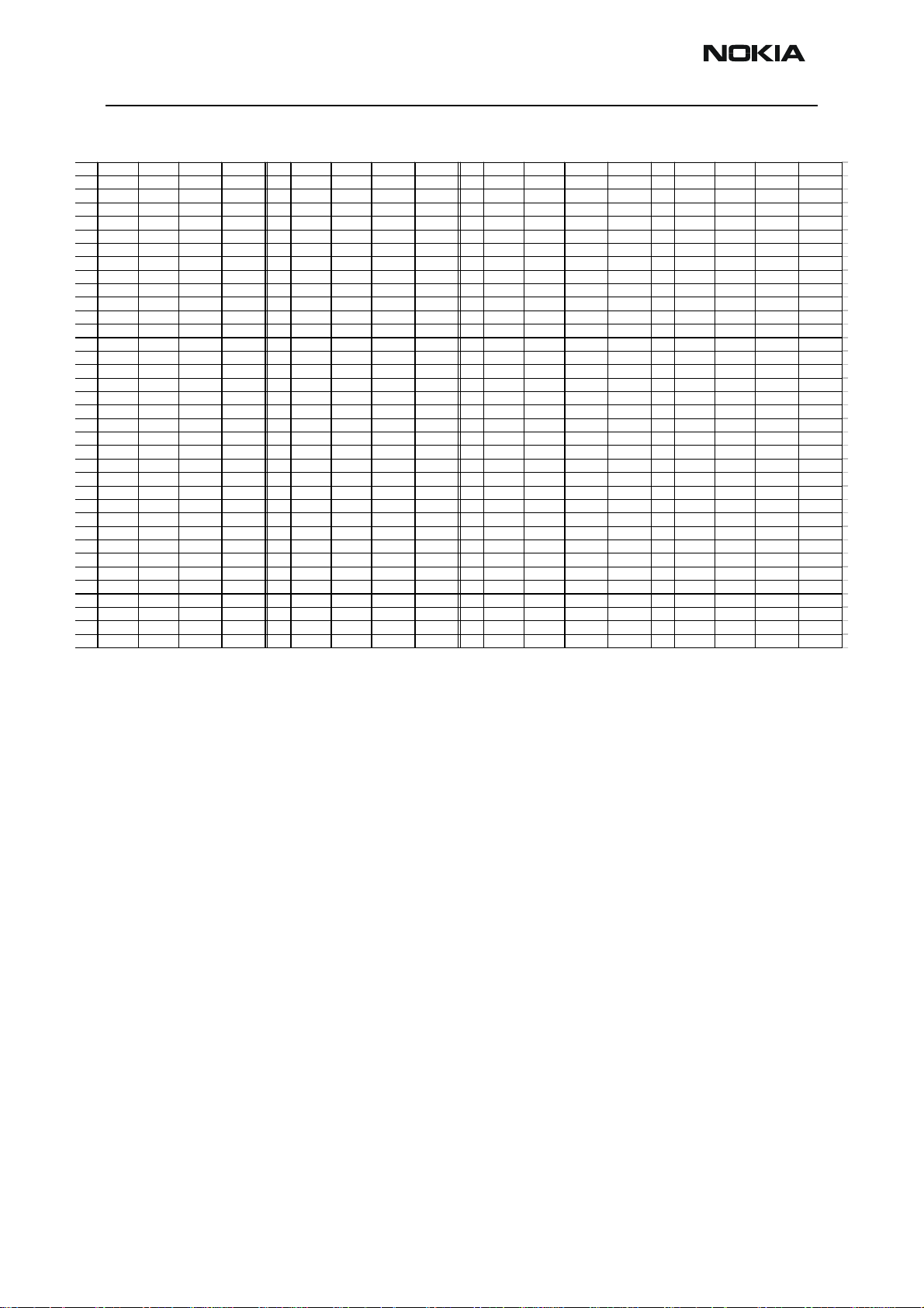
GSM900 (including EGSM900)
Fre quency list EGSM900
CH TX RX VCO TX VCO RX CH TX RX VCO TX VCO RX CH TX RX VCO TX VCO RX
975 880.2 925.2 3520.8 3700.8 1 890.2 935.2 3560.8 3740.8 63 902.6 947.6 3610.4 3790.4
976 880.4 925.4 3521.6 3701.6 2 890.4 935.4 3561.6 3741.6 64 902.8 947.8 3611.2 3791.2
977 880.6 925.6 3522.4 3702.4 3 890.6 935.6 3562.4 3742.4 65 903.0 948.0 3612.0 3792.0
978 880.8 925.8 3523.2 3703.2 4 890.8 935.8 3563.2 3743.2 66 903.2 948.2 3612.8 3792.8
979 881.0 926.0 3524.0 3704.0 5 891.0 936.0 3564.0 3744.0 67 903.4 948.4 3613.6 3793.6
980 881.2 926.2 3524.8 3704.8 6 891.2 936.2 3564.8 3744.8 68 903.6 948.6 3614.4 3794.4
981 881.4 926.4 3525.6 3705.6 7 891.4 936.4 3565.6 3745.6 69 903.8 948.8 3615.2 3795.2
982 881.6 926.6 3526.4 3706.4 8 891.6 936.6 3566.4 3746.4 70 904.0 949.0 3616.0 3796.0
983 881.8 926.8 3527.2 3707.2 9 891.8 936.8 3567.2 3747.2 71 904.2 949.2 3616.8 3796.8
984 882.0 927.0 3528.0 3708.0 10 892.0 937.0 3568.0 3748.0 72 904.4 949.4 3617.6 3797.6
985 882.2 927.2 3528.8 3708.8 11 892.2 937.2 3568.8 3748.8 73 904.6 949.6 3618.4 3798.4
986 882.4 927.4 3529.6 3709.6 12 892.4 937.4 3569.6 3749.6 74 904.8 949.8 3619.2 3799.2
987 882.6 927.6 3530.4 3710.4 13 892.6 937.6 3570.4 3750.4 75 905.0 950.0 3620.0 3800.0
988 882.8 927.8 3531.2 3711.2 14 892.8 937.8 3571.2 3751.2 76 905.2 950.2 3620.8 3800.8
989 883.0 928.0 3532.0 3712.0 15 893.0 938.0 3572.0 3752.0 77 905.4 950.4 3621.6 3801.6
990 883.2 928.2 3532.8 3712.8 16 893.2 938.2 3572.8 3752.8 78 905.6 950.6 3622.4 3802.4
991 883.4 928.4 3533.6 3713.6 17 893.4 938.4 3573.6 3753.6 79 905.8 950.8 3623.2 3803.2
992 883.6 928.6 3534.4 3714.4 18 893.6 938.6 3574.4 3754.4 80 906.0 951.0 3624.0 3804.0
993 883.8 928.8 3535.2 3715.2 19 893.8 938.8 3575.2 3755.2 81 906.2 951.2 3624.8 3804.8
994 884.0 929.0 3536.0 3716.0 20 894.0 939.0 3576.0 3756.0 82 906.4 951.4 3625.6 3805.6
995 884.2 929.2 3536.8 3716.8 21 894.2 939.2 3576.8 3756.8 83 906.6 951.6 3626.4 3806.4
996 884.4 929.4 3537.6 3717.6 22 894.4 939.4 3577.6 3757.6 84 906.8 951.8 3627.2 3807.2
997 884.6 929.6 3538.4 3718.4 23 894.6 939.6 3578.4 3758.4 85 907.0 952.0 3628.0 3808.0
998 884.8 929.8 3539.2 3719.2 24 894.8 939.8 3579.2 3759.2 86 907.2 952.2 3628.8 3808.8
999 885.0 930.0 3540.0 3720.0 25 895.0 940.0 3580.0 3760.0 87 907.4 952.4 3629.6 3809.6
1000 885.2 930.2 3540.8 3720.8 26 895.2 940.2 3580.8 3760.8 88 907.6 952.6 3630.4 3810.4
1001 885.4 930.4 3541.6 3721.6 27 895.4 940.4 3581.6 3761.6 89 907.8 952.8 3631.2 3811.2
1002 885.6 930.6 3542.4 3722.4 28 895.6 940.6 3582.4 3762.4 90 908.0 953.0 3632.0 3812.0
1003 885.8 930.8 3543.2 3723.2 29 895.8 940.8 3583.2 3763.2 91 908.2 953.2 3632.8 3812.8
1004 886.0 931.0 3544.0 3724.0 30 896.0 941.0 3584.0 3764.0 92 908.4 953.4 3633.6 3813.6
1005 886.2 931.2 3544.8 3724.8 31 896.2 941.2 3584.8 3764.8 93 908.6 953.6 3634.4 3814.4
1006 886.4 931.4 3545.6 3725.6 32 896.4 941.4 3585.6 3765.6 94 908.8 953.8 3635.2 3815.2
1007 886.6 931.6 3546.4 3726.4 33 896.6 941.6 3586.4 3766.4 95 909.0 954.0 3636.0 3816.0
1008 886.8 931.8 3547.2 3727.2 34 896.8 941.8 3587.2 3767.2 96 909.2 954.2 3636.8 3816.8
1009 887.0 932.0 3548.0 3728.0 35 897.0 942.0 3588.0 3768.0 97 909.4 954.4 3637.6 3817.6
1010 887.2 932.2 3548.8 3728.8 36 897.2 942.2 3588.8 3768.8 98 909.6 954.6 3638.4 3818.4
1011 887.4 932.4 3549.6 3729.6 37 897.4 942.4 3589.6 3769.6 99 909.8 954.8 3639.2 3819.2
1012 887.6 932.6 3550.4 3730.4 38 897.6 942.6 3590.4 3770.4 100 910.0 955.0 3640.0 3820.0
1013 887.8 932.8 3551.2 3731.2 39 897.8 942.8 3591.2 3771.2 101 910.2 955.2 3640.8 3820.8
1014 888.0 933.0 3552.0 3732.0 40 898.0 943.0 3592.0 3772.0 102 910.4 955.4 3641.6 3821.6
1015 888.2 933.2 3552.8 3732.8 41 898.2 943.2 3592.8 3772.8 103 910.6 955.6 3642.4 3822.4
1016 888.4 933.4 3553.6 3733.6 42 898.4 943.4 3593.6 3773.6 104 910.8 955.8 3643.2 3823.2
1017 888.6 933.6 3554.4 3734.4 43 898.6 943.6 3594.4 3774.4 105 911.0 956.0 3644.0 3824.0
1018 888.8 933.8 3555.2 3735.2 44 898.8 943.8 3595.2 3775.2 106 911.2 956.2 3644.8 3824.8
1019 889.0 934.0 3556.0 3736.0 45 899.0 944.0 3596.0 3776.0 107 911.4 956.4 3645.6 3825.6
1020 889.2 934.2 3556.8 3736.8 46 899.2 944.2 3596.8 3776.8 108 911.6 956.6 3646.4 3826.4
1021 889.4 934.4 3557.6 3737.6 47 899.4 944.4 3597.6 3777.6 109 911.8 956.8 3647.2 3827.2
1022 889.6 934.6 3558.4 3738.4 48 899.6 944.6 3598.4 3778.4 110 912.0 957.0 3648.0 3828.0
1023 889.8 934.8 3559.2 3739.2 49 899.8 944.8 3599.2 3779.2 111 912.2 957.2 3648.8 3828.8
0 890.0 935.0 3560.0 3740.0 50 900.0 945.0 3600.0 3780.0 112 912.4 957.4 3649.6 3829.6
51 900.2 945.2 3600.8 3780.8 113 912.6 957.6 3650.4 3830.4
52 900.4 945.4 3601.6 3781.6 114 912.8 957.8 3651.2 3831.2
53 900.6 945.6 3602.4 3782.4 115 913.0 958.0 3652.0 3832.0
54 900.8 945.8 3603.2 3783.2 116 913.2 958.2 3652.8 3832.8
55 901.0 946.0 3604.0 3784.0 117 913.4 958.4 3653.6 3833.6
56 901.2 946.2 3604.8 3784.8 118 913.6 958.6 3654.4 3834.4
57 901.4 946.4 3605.6 3785.6 119 913.8 958.8 3655.2 3835.2
58 901.6 946.6 3606.4 3786.4 120 914.0 959.0 3656.0 3836.0
59 901.8 946.8 3607.2 3787.2 121 914.2 959.2 3656.8 3836.8
60 902.0 947.0 3608.0 3788.0 122 914.4 959.4 3657.6 3837.6
61 902.2 947.2 3608.8 3788.8 123 914.6 959.6 3658.4 3838.4
62 902.4 947.4 3609.6 3789.6 124 914.8 959.8 3659.2 3839.2
Page 38 Nokia Corporation Issue 1 07/04
Page 39

RH-37
Nokia Customer Care 6(b) - RF Troubleshooting Instructions
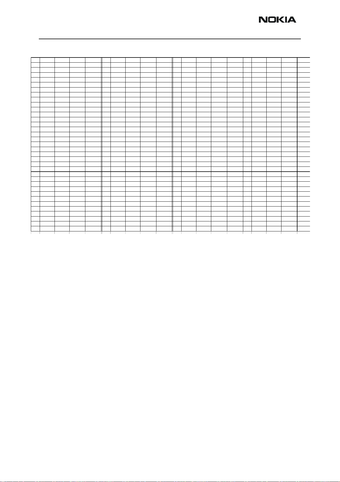
GSM1800
CH TX RX VCO TX VCO RX CH TX RX VCO TX VCO RX CH TX RX VCO TX VCO RX CH TX RX VCO TX VCO RX
Frequency list GSM1800
512
1710.2 1805.2 3420.4 3610.4
513
1710.4 1805.4 3420.8 3610.8
514
1710.6 1805.6 3421.2 3611.2
515
1710.8 1805.8 3421.6 3611.6
516
1711.0 1806.0 3422.0 3612.0
517
1711.2 1806.2 3422.4 3612.4
518
1711.4 1806.4 3422.8 3612.8
519
1711.6 1806.6 3423.2 3613.2
520
1711.8 1806.8 3423.6 3613.6
521
1712.0 1807.0 3424.0 3614.0
522
1712.2 1807.2 3424.4 3614.4
523
1712.4 1807.4 3424.8 3614.8
524
1712.6 1807.6 3425.2 3615.2
525
1712.8 1807.8 3425.6 3615.6
526
1713.0 1808.0 3426.0 3616.0
527
1713.2 1808.2 3426.4 3616.4
528
1713.4 1808.4 3426.8 3616.8
529
1713.6 1808.6 3427.2 3617.2
530
1713.8 1808.8 3427.6 3617.6
531
1714.0 1809.0 3428.0 3618.0
532
1714.2 1809.2 3428.4 3618.4
533
1714.4 1809.4 3428.8 3618.8
534
1714.6 1809.6 3429.2 3619.2
535
1714.8 1809.8 3429.6 3619.6
536
1715.0 1810.0 3430.0 3620.0
537
1715.2 1810.2 3430.4 3620.4
538
1715.4 1810.4 3430.8 3620.8
539
1715.6 1810.6 3431.2 3621.2
540
1715.8 1810.8 3431.6 3621.6
541
1716.0 1811.0 3432.0 3622.0
542
1716.2 1811.2 3432.4 3622.4
543
1716.4 1811.4 3432.8 3622.8
544
1716.6 1811.6 3433.2 3623.2
545
1716.8 1811.8 3433.6 3623.6
546
1717.0 1812.0 3434.0 3624.0
547
1717.2 1812.2 3434.4 3624.4
548
1717.4 1812.4 3434.8 3624.8
549
1717.6 1812.6 3435.2 3625.2
550
1717.8 1812.8 3435.6 3625.6
551
1718.0 1813.0 3436.0 3626.0
552
1718.2 1813.2 3436.4 3626.4
553
1718.4 1813.4 3436.8 3626.8
554
1718.6 1813.6 3437.2 3627.2
555
1718.8 1813.8 3437.6 3627.6
556
1719.0 1814.0 3438.0 3628.0
557
1719.2 1814.2 3438.4 3628.4
558
1719.4 1814.4 3438.8 3628.8
559
1719.6 1814.6 3439.2 3629.2
560
1719.8 1814.8 3439.6 3629.6
561
1720.0 1815.0 3440.0 3630.0
562
1720.2 1815.2 3440.4 3630.4
563
1720.4 1815.4 3440.8 3630.8
564
1720.6 1815.6 3441.2 3631.2
565
1720.8 1815.8 3441.6 3631.6
566
1721.0 1816.0 3442.0 3632.0
567
1721.2 1816.2 3442.4 3632.4
568
1721.4 1816.4 3442.8 3632.8
569
1721.6 1816.6 3443.2 3633.2
570
1721.8 1816.8 3443.6 3633.6
606
1729.0 1824.0 3458.0 3648.0
607
1729.2 1824.2 3458.4 3648.4
608
1729.4 1824.4 3458.8 3648.8
609
1729.6 1824.6 3459.2 3649.2
610
1729.8 1824.8 3459.6 3649.6
611
1730.0 1825.0 3460.0 3650.0
612
1730.2 1825.2 3460.4 3650.4
613
1730.4 1825.4 3460.8 3650.8
614
1730.6 1825.6 3461.2 3651.2
615
1730.8 1825.8 3461.6 3651.6
616
1731.0 1826.0 3462.0 3652.0
617
1731.2 1826.2 3462.4 3652.4
618
1731.4 1826.4 3462.8 3652.8
619
1731.6 1826.6 3463.2 3653.2
620
1731.8 1826.8 3463.6 3653.6
621
1732.0 1827.0 3464.0 3654.0
622
1732.2 1827.2 3464.4 3654.4
623
1732.4 1827.4 3464.8 3654.8
624
1732.6 1827.6 3465.2 3655.2
625
1732.8 1827.8 3465.6 3655.6
626
1733.0 1828.0 3466.0 3656.0
627
1733.2 1828.2 3466.4 3656.4
628
1733.4 1828.4 3466.8 3656.8
629
1733.6 1828.6 3467.2 3657.2
630
1733.8 1828.8 3467.6 3657.6
631
1734.0 1829.0 3468.0 3658.0
632
1734.2 1829.2 3468.4 3658.4
633
1734.4 1829.4 3468.8 3658.8
634
1734.6 1829.6 3469.2 3659.2
635
1734.8 1829.8 3469.6 3659.6
636
1735.0 1830.0 3470.0 3660.0
637
1735.2 1830.2 3470.4 3660.4
638
1735.4 1830.4 3470.8 3660.8
639
1735.6 1830.6 3471.2 3661.2
640
1735.8 1830.8 3471.6 3661.6
641
1736.0 1831.0 3472.0 3662.0
642
1736.2 1831.2 3472.4 3662.4
643
1736.4 1831.4 3472.8 3662.8
644
1736.6 1831.6 3473.2 3663.2
645
1736.8 1831.8 3473.6 3663.6
646
1737.0 1832.0 3474.0 3664.0
647
1737.2 1832.2 3474.4 3664.4
648
1737.4 1832.4 3474.8 3664.8
649
1737.6 1832.6 3475.2 3665.2
650
1737.8 1832.8 3475.6 3665.6
651
1738.0 1833.0 3476.0 3666.0
652
1738.2 1833.2 3476.4 3666.4
653
1738.4 1833.4 3476.8 3666.8
654
1738.6 1833.6 3477.2 3667.2
655
1738.8 1833.8 3477.6 3667.6
656
1739.0 1834.0 3478.0 3668.0
657
1739.2 1834.2 3478.4 3668.4
658
1739.4 1834.4 3478.8 3668.8
659
1739.6 1834.6 3479.2 3669.2
660
1739.8 1834.8 3479.6 3669.6
661
1740.0 1835.0 3480.0 3670.0
662
1740.2 1835.2 3480.4 3670.4
663
1740.4 1835.4 3480.8 3670.8
664
1740.6 1835.6 3481.2 3671.2
700
1747.8 1842.8 3495.6 3685.6
701
1748.0 1843.0 3496.0 3686.0
702
1748.2 1843.2 3496.4 3686.4
703
1748.4 1843.4 3496.8 3686.8
704
1748.6 1843.6 3497.2 3687.2
705
1748.8 1843.8 3497.6 3687.6
706
1749.0 1844.0 3498.0 3688.0
707
1749.2 1844.2 3498.4 3688.4
708
1749.4 1844.4 3498.8 3688.8
709
1749.6 1844.6 3499.2 3689.2
710
1749.8 1844.8 3499.6 3689.6
711
1750.0 1845.0 3500.0 3690.0
712
1750.2 1845.2 3500.4 3690.4
713
1750.4 1845.4 3500.8 3690.8
714
1750.6 1845.6 3501.2 3691.2
715
1750.8 1845.8 3501.6 3691.6
716
1751.0 1846.0 3502.0 3692.0
717
1751.2 1846.2 3502.4 3692.4
718
1751.4 1846.4 3502.8 3692.8
719
1751.6 1846.6 3503.2 3693.2
720
1751.8 1846.8 3503.6 3693.6
721
1752.0 1847.0 3504.0 3694.0
722
1752.2 1847.2 3504.4 3694.4
723
1752.4 1847.4 3504.8 3694.8
724
1752.6 1847.6 3505.2 3695.2
725
1752.8 1847.8 3505.6 3695.6
726
1753.0 1848.0 3506.0 3696.0
727
1753.2 1848.2 3506.4 3696.4
728
1753.4 1848.4 3506.8 3696.8
729
1753.6 1848.6 3507.2 3697.2
730
1753.8 1848.8 3507.6 3697.6
731
1754.0 1849.0 3508.0 3698.0
732
1754.2 1849.2 3508.4 3698.4
733
1754.4 1849.4 3508.8 3698.8
734
1754.6 1849.6 3509.2 3699.2
735
1754.8 1849.8 3509.6 3699.6
736
1755.0 1850.0 3510.0 3700.0
737
1755.2 1850.2 3510.4 3700.4
738
1755.4 1850.4 3510.8 3700.8
739
1755.6 1850.6 3511.2 3701.2
740
1755.8 1850.8 3511.6 3701.6
741
1756.0 1851.0 3512.0 3702.0
742
1756.2 1851.2 3512.4 3702.4
743
1756.4 1851.4 3512.8 3702.8
744
1756.6 1851.6 3513.2 3703.2
745
1756.8 1851.8 3513.6 3703.6
746
1757.0 1852.0 3514.0 3704.0
747
1757.2 1852.2 3514.4 3704.4
748
1757.4 1852.4 3514.8 3704.8
749
1757.6 1852.6 3515.2 3705.2
750
1757.8 1852.8 3515.6 3705.6
751
1758.0 1853.0 3516.0 3706.0
752
1758.2 1853.2 3516.4 3706.4
753
1758.4 1853.4 3516.8 3706.8
754
1758.6 1853.6 3517.2 3707.2
755
1758.8 1853.8 3517.6 3707.6
756
1759.0 1854.0 3518.0 3708.0
757
1759.2 1854.2 3518.4 3708.4
758
1759.4 1854.4 3518.8 3708.8
794
1766.6 1861.6 3533.2 3723.2
795
1766.8 1861.8 3533.6 3723.6
796
1767.0 1862.0 3534.0 3724.0
797
1767.2 1862.2 3534.4 3724.4
798
1767.4 1862.4 3534.8 3724.8
799
1767.6 1862.6 3535.2 3725.2
800
1767.8 1862.8 3535.6 3725.6
801
1768.0 1863.0 3536.0 3726.0
802
1768.2 1863.2 3536.4 3726.4
803
1768.4 1863.4 3536.8 3726.8
804
1768.6 1863.6 3537.2 3727.2
805
1768.8 1863.8 3537.6 3727.6
806
1769.0 1864.0 3538.0 3728.0
807
1769.2 1864.2 3538.4 3728.4
808
1769.4 1864.4 3538.8 3728.8
809
1769.6 1864.6 3539.2 3729.2
810
1769.8 1864.8 3539.6 3729.6
811
1770.0 1865.0 3540.0 3730.0
812
1770.2 1865.2 3540.4 3730.4
813
1770.4 1865.4 3540.8 3730.8
814
1770.6 1865.6 3541.2 3731.2
815
1770.8 1865.8 3541.6 3731.6
816
1771.0 1866.0 3542.0 3732.0
817
1771.2 1866.2 3542.4 3732.4
818
1771.4 1866.4 3542.8 3732.8
819
1771.6 1866.6 3543.2 3733.2
820
1771.8 1866.8 3543.6 3733.6
821
1772.0 1867.0 3544.0 3734.0
822
1772.2 1867.2 3544.4 3734.4
823
1772.4 1867.4 3544.8 3734.8
824
1772.6 1867.6 3545.2 3735.2
825
1772.8 1867.8 3545.6 3735.6
826
1773.0 1868.0 3546.0 3736.0
827
1773.2 1868.2 3546.4 3736.4
828
1773.4 1868.4 3546.8 3736.8
829
1773.6 1868.6 3547.2 3737.2
830
1773.8 1868.8 3547.6 3737.6
831
1774.0 1869.0 3548.0 3738.0
832
1774.2 1869.2 3548.4 3738.4
833
1774.4 1869.4 3548.8 3738.8
834
1774.6 1869.6 3549.2 3739.2
835
1774.8 1869.8 3549.6 3739.6
836
1775.0 1870.0 3550.0 3740.0
837
1775.2 1870.2 3550.4 3740.4
838
1775.4 1870.4 3550.8 3740.8
839
1775.6 1870.6 3551.2 3741.2
840
1775.8 1870.8 3551.6 3741.6
841
1776.0 1871.0 3552.0 3742.0
842
1776.2 1871.2 3552.4 3742.4
843
1776.4 1871.4 3552.8 3742.8
844
1776.6 1871.6 3553.2 3743.2
845
1776.8 1871.8 3553.6 3743.6
846
1777.0 1872.0 3554.0 3744.0
847
1777.2 1872.2 3554.4 3744.4
848
1777.4 1872.4 3554.8 3744.8
849
1777.6 1872.6 3555.2 3745.2
850
1777.8 1872.8 3555.6 3745.6
851
1778.0 1873.0 3556.0 3746.0
852
1778.2 1873.2 3556.4 3746.4
Issue 1 07/04 Nokia Corporation Page 39
Page 40
RH-37
6(b) - RF Troubleshooting Instructions Nokia Customer Care
570
1721.8 1816.8 3443.6 3633.6
571
1722.0 1817.0 3444.0 3634.0
572
1722.2 1817.2 3444.4 3634.4
573
1722.4 1817.4 3444.8 3634.8
574
1722.6 1817.6 3445.2 3635.2
575
1722.8 1817.8 3445.6 3635.6
576
1723.0 1818.0 3446.0 3636.0
577
1723.2 1818.2 3446.4 3636.4
578
1723.4 1818.4 3446.8 3636.8
579
1723.6 1818.6 3447.2 3637.2
580
1723.8 1818.8 3447.6 3637.6
581
1724.0 1819.0 3448.0 3638.0
582
1724.2 1819.2 3448.4 3638.4
583
1724.4 1819.4 3448.8 3638.8
584
1724.6 1819.6 3449.2 3639.2
585
1724.8 1819.8 3449.6 3639.6
586
1725.0 1820.0 3450.0 3640.0
587
1725.2 1820.2 3450.4 3640.4
588
1725.4 1820.4 3450.8 3640.8
589
1725.6 1820.6 3451.2 3641.2
590
1725.8 1820.8 3451.6 3641.6
591
1726.0 1821.0 3452.0 3642.0
592
1726.2 1821.2 3452.4 3642.4
593
1726.4 1821.4 3452.8 3642.8
594
1726.6 1821.6 3453.2 3643.2
595
1726.8 1821.8 3453.6 3643.6
596
1727.0 1822.0 3454.0 3644.0
597
1727.2 1822.2 3454.4 3644.4
598
1727.4 1822.4 3454.8 3644.8
599
1727.6 1822.6 3455.2 3645.2
600
1727.8 1822.8 3455.6 3645.6
601
1728.0 1823.0 3456.0 3646.0
602
1728.2 1823.2 3456.4 3646.4
603
1728.4 1823.4 3456.8 3646.8
604
1728.6 1823.6 3457.2 3647.2
605
1728.8 1823.8 3457.6 3647.6
664
1740.6 1835.6 3481.2 3671.2
665
1740.8 1835.8 3481.6 3671.6
666
1741.0 1836.0 3482.0 3672.0
667
1741.2 1836.2 3482.4 3672.4
668
1741.4 1836.4 3482.8 3672.8
669
1741.6 1836.6 3483.2 3673.2
670
1741.8 1836.8 3483.6 3673.6
671
1742.0 1837.0 3484.0 3674.0
672
1742.2 1837.2 3484.4 3674.4
673
1742.4 1837.4 3484.8 3674.8
674
1742.6 1837.6 3485.2 3675.2
675
1742.8 1837.8 3485.6 3675.6
676
1743.0 1838.0 3486.0 3676.0
677
1743.2 1838.2 3486.4 3676.4
678
1743.4 1838.4 3486.8 3676.8
679
1743.6 1838.6 3487.2 3677.2
680
1743.8 1838.8 3487.6 3677.6
681
1744.0 1839.0 3488.0 3678.0
682
1744.2 1839.2 3488.4 3678.4
683
1744.4 1839.4 3488.8 3678.8
684
1744.6 1839.6 3489.2 3679.2
685
1744.8 1839.8 3489.6 3679.6
686
1745.0 1840.0 3490.0 3680.0
687
1745.2 1840.2 3490.4 3680.4
688
1745.4 1840.4 3490.8 3680.8
689
1745.6 1840.6 3491.2 3681.2
690
1745.8 1840.8 3491.6 3681.6
691
1746.0 1841.0 3492.0 3682.0
692
1746.2 1841.2 3492.4 3682.4
693
1746.4 1841.4 3492.8 3682.8
694
1746.6 1841.6 3493.2 3683.2
695
1746.8 1841.8 3493.6 3683.6
696
1747.0 1842.0 3494.0 3684.0
697
1747.2 1842.2 3494.4 3684.4
698
1747.4 1842.4 3494.8 3684.8
699
1747.6 1842.6 3495.2 3685.2
758
1759.4 1854.4 3518.8 3708.8
759
1759.6 1854.6 3519.2 3709.2
760
1759.8 1854.8 3519.6 3709.6
761
1760.0 1855.0 3520.0 3710.0
762
1760.2 1855.2 3520.4 3710.4
763
1760.4 1855.4 3520.8 3710.8
764
1760.6 1855.6 3521.2 3711.2
765
1760.8 1855.8 3521.6 3711.6
766
1761.0 1856.0 3522.0 3712.0
767
1761.2 1856.2 3522.4 3712.4
768
1761.4 1856.4 3522.8 3712.8
769
1761.6 1856.6 3523.2 3713.2
770
1761.8 1856.8 3523.6 3713.6
771
1762.0 1857.0 3524.0 3714.0
772
1762.2 1857.2 3524.4 3714.4
773
1762.4 1857.4 3524.8 3714.8
774
1762.6 1857.6 3525.2 3715.2
775
1762.8 1857.8 3525.6 3715.6
776
1763.0 1858.0 3526.0 3716.0
777
1763.2 1858.2 3526.4 3716.4
778
1763.4 1858.4 3526.8 3716.8
779
1763.6 1858.6 3527.2 3717.2
780
1763.8 1858.8 3527.6 3717.6
781
1764.0 1859.0 3528.0 3718.0
782
1764.2 1859.2 3528.4 3718.4
783
1764.4 1859.4 3528.8 3718.8
784
1764.6 1859.6 3529.2 3719.2
785
1764.8 1859.8 3529.6 3719.6
786
1765.0 1860.0 3530.0 3720.0
787
1765.2 1860.2 3530.4 3720.4
788
1765.4 1860.4 3530.8 3720.8
789
1765.6 1860.6 3531.2 3721.2
790
1765.8 1860.8 3531.6 3721.6
791
1766.0 1861.0 3532.0 3722.0
792
1766.2 1861.2 3532.4 3722.4
793
1766.4 1861.4 3532.8 3722.8
852
1778.2 1873.2 3556.4 3746.4
853
1778.4 1873.4 3556.8 3746.8
854
1778.6 1873.6 3557.2 3747.2
855
1778.8 1873.8 3557.6 3747.6
856
1779.0 1874.0 3558.0 3748.0
857
1779.2 1874.2 3558.4 3748.4
858
1779.4 1874.4 3558.8 3748.8
859
1779.6 1874.6 3559.2 3749.2
860
1779.8 1874.8 3559.6 3749.6
861
1780.0 1875.0 3560.0 3750.0
862
1780.2 1875.2 3560.4 3750.4
863
1780.4 1875.4 3560.8 3750.8
864
1780.6 1875.6 3561.2 3751.2
865
1780.8 1875.8 3561.6 3751.6
866
1781.0 1876.0 3562.0 3752.0
867
1781.2 1876.2 3562.4 3752.4
868
1781.4 1876.4 3562.8 3752.8
869
1781.6 1876.6 3563.2 3753.2
870
1781.8 1876.8 3563.6 3753.6
871
1782.0 1877.0 3564.0 3754.0
872
1782.2 1877.2 3564.4 3754.4
873
1782.4 1877.4 3564.8 3754.8
874
1782.6 1877.6 3565.2 3755.2
875
1782.8 1877.8 3565.6 3755.6
876
1783.0 1878.0 3566.0 3756.0
877
1783.2 1878.2 3566.4 3756.4
878
1783.4 1878.4 3566.8 3756.8
879
1783.6 1878.6 3567.2 3757.2
880
1783.8 1878.8 3567.6 3757.6
881
1784.0 1879.0 3568.0 3758.0
882
1784.2 1879.2 3568.4 3758.4
883
1784.4 1879.4 3568.8 3758.8
884
1784.6 1879.6 3569.2 3759.2
885
1784.8 1879.8 3569.6 3759.6
Page 40 Nokia Corporation Issue 1 07/04
Page 41

RH-37
Nokia Customer Care 6(b) - RF Troubleshooting Instructions
GSM1900
CH TX RX VCO TX VCO RX CH T X RX VCO TX VCO RX CH TX RX VCO TX VCO RX CH TX RX VCO TX VCO RX
512
1850.2 1930.2 3700.4 3860.4
513
1850.4 1930.4 3700.8 3860.8
514
1850.6 1930.6 3701.2 3861.2
515
1850.8 1930.8 3701.6 3861.6
516
1851.0 1931.0 3702.0 3862.0
517
1851.2 1931.2 3702.4 3862.4
518
1851.4 1931.4 3702.8 3862.8
519
1851.6 1931.6 3703.2 3863.2
520
1851.8 1931.8 3703.6 3863.6
521
1852.0 1932.0 3704.0 3864.0
522
1852.2 1932.2 3704.4 3864.4
523
1852.4 1932.4 3704.8 3864.8
524
1852.6 1932.6 3705.2 3865.2
525
1852.8 1932.8 3705.6 3865.6
526
1853.0 1933.0 3706.0 3866.0
527
1853.2 1933.2 3706.4 3866.4
528
1853.4 1933.4 3706.8 3866.8
529
1853.6 1933.6 3707.2 3867.2
530
1853.8 1933.8 3707.6 3867.6
531
1854.0 1934.0 3708.0 3868.0
532
1854.2 1934.2 3708.4 3868.4
533
1854.4 1934.4 3708.8 3868.8
534
1854.6 1934.6 3709.2 3869.2
535
1854.8 1934.8 3709.6 3869.6
536
1855.0 1935.0 3710.0 3870.0
537
1855.2 1935.2 3710.4 3870.4
538
1855.4 1935.4 3710.8 3870.8
539
1855.6 1935.6 3711.2 3871.2
540
1855.8 1935.8 3711.6 3871.6
541
1856.0 1936.0 3712.0 3872.0
542
1856.2 1936.2 3712.4 3872.4
543
1856.4 1936.4 3712.8 3872.8
544
1856.6 1936.6 3713.2 3873.2
545
1856.8 1936.8 3713.6 3873.6
546
1857.0 1937.0 3714.0 3874.0
547
1857.2 1937.2 3714.4 3874.4
548
1857.4 1937.4 3714.8 3874.8
549
1857.6 1937.6 3715.2 3875.2
550
1857.8 1937.8 3715.6 3875.6
551
1858.0 1938.0 3716.0 3876.0
552
1858.2 1938.2 3716.4 3876.4
553
1858.4 1938.4 3716.8 3876.8
554
1858.6 1938.6 3717.2 3877.2
555
1858.8 1938.8 3717.6 3877.6
556
1859.0 1939.0 3718.0 3878.0
557
1859.2 1939.2 3718.4 3878.4
558
1859.4 1939.4 3718.8 3878.8
559
1859.6 1939.6 3719.2 3879.2
560
1859.8 1939.8 3719.6 3879.6
561
1860.0 1940.0 3720.0 3880.0
562
1860.2 1940.2 3720.4 3880.4
563
1860.4 1940.4 3720.8 3880.8
564
1860.6 1940.6 3721.2 3881.2
565
1860.8 1940.8 3721.6 3881.6
566
1861.0 1941.0 3722.0 3882.0
567
1861.2 1941.2 3722.4 3882.4
568
1861.4 1941.4 3722.8 3882.8
569
1861.6 1941.6 3723.2 3883.2
570
1861.8 1941.8 3723.6 3883.6
606
1869.0 1949.0 3738.0 3898.0
607
1869.2 1949.2 3738.4 3898.4
608
1869.4 1949.4 3738.8 3898.8
609
1869.6 1949.6 3739.2 3899.2
610
1869.8 1949.8 3739.6 3899.6
611
1870.0 1950.0 3740.0 3900.0
612
1870.2 1950.2 3740.4 3900.4
613
1870.4 1950.4 3740.8 3900.8
614
1870.6 1950.6 3741.2 3901.2
615
1870.8 1950.8 3741.6 3901.6
616
1871.0 1951.0 3742.0 3902.0
617
1871.2 1951.2 3742.4 3902.4
618
1871.4 1951.4 3742.8 3902.8
619
1871.6 1951.6 3743.2 3903.2
620
1871.8 1951.8 3743.6 3903.6
621
1872.0 1952.0 3744.0 3904.0
622
1872.2 1952.2 3744.4 3904.4
623
1872.4 1952.4 3744.8 3904.8
624
1872.6 1952.6 3745.2 3905.2
625
1872.8 1952.8 3745.6 3905.6
626
1873.0 1953.0 3746.0 3906.0
627
1873.2 1953.2 3746.4 3906.4
628
1873.4 1953.4 3746.8 3906.8
629
1873.6 1953.6 3747.2 3907.2
630
1873.8 1953.8 3747.6 3907.6
631
1874.0 1954.0 3748.0 3908.0
632
1874.2 1954.2 3748.4 3908.4
633
1874.4 1954.4 3748.8 3908.8
634
1874.6 1954.6 3749.2 3909.2
635
1874.8 1954.8 3749.6 3909.6
636
1875.0 1955.0 3750.0 3910.0
637
1875.2 1955.2 3750.4 3910.4
638
1875.4 1955.4 3750.8 3910.8
639
1875.6 1955.6 3751.2 3911.2
640
1875.8 1955.8 3751.6 3911.6
641
1876.0 1956.0 3752.0 3912.0
642
1876.2 1956.2 3752.4 3912.4
643
1876.4 1956.4 3752.8 3912.8
644
1876.6 1956.6 3753.2 3913.2
645
1876.8 1956.8 3753.6 3913.6
646
1877.0 1957.0 3754.0 3914.0
647
1877.2 1957.2 3754.4 3914.4
648
1877.4 1957.4 3754.8 3914.8
649
1877.6 1957.6 3755.2 3915.2
650
1877.8 1957.8 3755.6 3915.6
651
1878.0 1958.0 3756.0 3916.0
652
1878.2 1958.2 3756.4 3916.4
653
1878.4 1958.4 3756.8 3916.8
654
1878.6 1958.6 3757.2 3917.2
655
1878.8 1958.8 3757.6 3917.6
656
1879.0 1959.0 3758.0 3918.0
657
1879.2 1959.2 3758.4 3918.4
658
1879.4 1959.4 3758.8 3918.8
659
1879.6 1959.6 3759.2 3919.2
660
1879.8 1959.8 3759.6 3919.6
661
1880.0 1960.0 3760.0 3920.0
662
1880.2 1960.2 3760.4 3920.4
663
1880.4 1960.4 3760.8 3920.8
664
1880.6 1960.6 3761.2 3921.2
Freque ncy list NPL-2 GSM1900
700
1887.8 1967.8 3775.6 3935.6
701
1888.0 1968.0 3776.0 3936.0
702
1888.2 1968.2 3776.4 3936.4
703
1888.4 1968.4 3776.8 3936.8
704
1888.6 1968.6 3777.2 3937.2
705
1888.8 1968.8 3777.6 3937.6
706
1889.0 1969.0 3778.0 3938.0
707
1889.2 1969.2 3778.4 3938.4
708
1889.4 1969.4 3778.8 3938.8
709
1889.6 1969.6 3779.2 3939.2
710
1889.8 1969.8 3779.6 3939.6
711
1890.0 1970.0 3780.0 3940.0
712
1890.2 1970.2 3780.4 3940.4
713
1890.4 1970.4 3780.8 3940.8
714
1890.6 1970.6 3781.2 3941.2
715
1890.8 1970.8 3781.6 3941.6
716
1891.0 1971.0 3782.0 3942.0
717
1891.2 1971.2 3782.4 3942.4
718
1891.4 1971.4 3782.8 3942.8
719
1891.6 1971.6 3783.2 3943.2
720
1891.8 1971.8 3783.6 3943.6
721
1892.0 1972.0 3784.0 3944.0
722
1892.2 1972.2 3784.4 3944.4
723
1892.4 1972.4 3784.8 3944.8
724
1892.6 1972.6 3785.2 3945.2
725
1892.8 1972.8 3785.6 3945.6
726
1893.0 1973.0 3786.0 3946.0
727
1893.2 1973.2 3786.4 3946.4
728
1893.4 1973.4 3786.8 3946.8
729
1893.6 1973.6 3787.2 3947.2
730
1893.8 1973.8 3787.6 3947.6
731
1894.0 1974.0 3788.0 3948.0
732
1894.2 1974.2 3788.4 3948.4
733
1894.4 1974.4 3788.8 3948.8
734
1894.6 1974.6 3789.2 3949.2
735
1894.8 1974.8 3789.6 3949.6
736
1895.0 1975.0 3790.0 3950.0
737
1895.2 1975.2 3790.4 3950.4
738
1895.4 1975.4 3790.8 3950.8
739
1895.6 1975.6 3791.2 3951.2
740
1895.8 1975.8 3791.6 3951.6
741
1896.0 1976.0 3792.0 3952.0
742
1896.2 1976.2 3792.4 3952.4
743
1896.4 1976.4 3792.8 3952.8
744
1896.6 1976.6 3793.2 3953.2
745
1896.8 1976.8 3793.6 3953.6
746
1897.0 1977.0 3794.0 3954.0
747
1897.2 1977.2 3794.4 3954.4
748
1897.4 1977.4 3794.8 3954.8
749
1897.6 1977.6 3795.2 3955.2
750
1897.8 1977.8 3795.6 3955.6
751
1898.0 1978.0 3796.0 3956.0
752
1898.2 1978.2 3796.4 3956.4
753
1898.4 1978.4 3796.8 3956.8
754
1898.6 1978.6 3797.2 3957.2
755
1898.8 1978.8 3797.6 3957.6
756
1899.0 1979.0 3798.0 3958.0
757
1899.2 1979.2 3798.4 3958.4
758
1899.4 1979.4 3798.8 3958.8
794
1906.6 1986.6 3813.2 3973.2
795
1906.8 1986.8 3813.6 3973.6
796
1907.0 1987.0 3814.0 3974.0
797
1907.2 1987.2 3814.4 3974.4
798
1907.4 1987.4 3814.8 3974.8
799
1907.6 1987.6 3815.2 3975.2
800
1907.8 1987.8 3815.6 3975.6
801
1908.0 1988.0 3816.0 3976.0
802
1908.2 1988.2 3816.4 3976.4
803
1908.4 1988.4 3816.8 3976.8
804
1908.6 1988.6 3817.2 3977.2
805
1908.8 1988.8 3817.6 3977.6
806
1909.0 1989.0 3818.0 3978.0
807
1909.2 1989.2 3818.4 3978.4
808
1909.4 1989.4 3818.8 3978.8
809
1909.6 1989.6 3819.2 3979.2
810
1909.8 1989.8 3819.6 3979.6
Issue 1 07/04 Nokia Corporation Page 41
Page 42
RH-37
6(b) - RF Troubleshooting Instructions Nokia Customer Care
571
1862.0 1942.0 3724.0 3884.0
572
1862.2 1942.2 3724.4 3884.4
573
1862.4 1942.4 3724.8 3884.8
574
1862.6 1942.6 3725.2 3885.2
575
1862.8 1942.8 3725.6 3885.6
576
1863.0 1943.0 3726.0 3886.0
577
1863.2 1943.2 3726.4 3886.4
578
1863.4 1943.4 3726.8 3886.8
579
1863.6 1943.6 3727.2 3887.2
580
1863.8 1943.8 3727.6 3887.6
581
1864.0 1944.0 3728.0 3888.0
582
1864.2 1944.2 3728.4 3888.4
583
1864.4 1944.4 3728.8 3888.8
584
1864.6 1944.6 3729.2 3889.2
585
1864.8 1944.8 3729.6 3889.6
586
1865.0 1945.0 3730.0 3890.0
587
1865.2 1945.2 3730.4 3890.4
588
1865.4 1945.4 3730.8 3890.8
589
1865.6 1945.6 3731.2 3891.2
590
1865.8 1945.8 3731.6 3891.6
591
1866.0 1946.0 3732.0 3892.0
592
1866.2 1946.2 3732.4 3892.4
593
1866.4 1946.4 3732.8 3892.8
594
1866.6 1946.6 3733.2 3893.2
595
1866.8 1946.8 3733.6 3893.6
596
1867.0 1947.0 3734.0 3894.0
597
1867.2 1947.2 3734.4 3894.4
598
1867.4 1947.4 3734.8 3894.8
599
1867.6 1947.6 3735.2 3895.2
600
1867.8 1947.8 3735.6 3895.6
601
1868.0 1948.0 3736.0 3896.0
602
1868.2 1948.2 3736.4 3896.4
603
1868.4 1948.4 3736.8 3896.8
604
1868.6 1948.6 3737.2 3897.2
605
1868.8 1948.8 3737.6 3897.6
665
1880.8 1960.8 3761.6 3921.6
666
1881.0 1961.0 3762.0 3922.0
667
1881.2 1961.2 3762.4 3922.4
668
1881.4 1961.4 3762.8 3922.8
669
1881.6 1961.6 3763.2 3923.2
670
1881.8 1961.8 3763.6 3923.6
671
1882.0 1962.0 3764.0 3924.0
672
1882.2 1962.2 3764.4 3924.4
673
1882.4 1962.4 3764.8 3924.8
674
1882.6 1962.6 3765.2 3925.2
675
1882.8 1962.8 3765.6 3925.6
676
1883.0 1963.0 3766.0 3926.0
677
1883.2 1963.2 3766.4 3926.4
678
1883.4 1963.4 3766.8 3926.8
679
1883.6 1963.6 3767.2 3927.2
680
1883.8 1963.8 3767.6 3927.6
681
1884.0 1964.0 3768.0 3928.0
682
1884.2 1964.2 3768.4 3928.4
683
1884.4 1964.4 3768.8 3928.8
684
1884.6 1964.6 3769.2 3929.2
685
1884.8 1964.8 3769.6 3929.6
686
1885.0 1965.0 3770.0 3930.0
687
1885.2 1965.2 3770.4 3930.4
688
1885.4 1965.4 3770.8 3930.8
689
1885.6 1965.6 3771.2 3931.2
690
1885.8 1965.8 3771.6 3931.6
691
1886.0 1966.0 3772.0 3932.0
692
1886.2 1966.2 3772.4 3932.4
693
1886.4 1966.4 3772.8 3932.8
694
1886.6 1966.6 3773.2 3933.2
695
1886.8 1966.8 3773.6 3933.6
696
1887.0 1967.0 3774.0 3934.0
697
1887.2 1967.2 3774.4 3934.4
698
1887.4 1967.4 3774.8 3934.8
699
1887.6 1967.6 3775.2 3935.2
759
1899.6 1979.6 3799.2 3959.2
760
1899.8 1979.8 3799.6 3959.6
761
1900.0 1980.0 3800.0 3960.0
762
1900.2 1980.2 3800.4 3960.4
763
1900.4 1980.4 3800.8 3960.8
764
1900.6 1980.6 3801.2 3961.2
765
1900.8 1980.8 3801.6 3961.6
766
1901.0 1981.0 3802.0 3962.0
767
1901.2 1981.2 3802.4 3962.4
768
1901.4 1981.4 3802.8 3962.8
769
1901.6 1981.6 3803.2 3963.2
770
1901.8 1981.8 3803.6 3963.6
771
1902.0 1982.0 3804.0 3964.0
772
1902.2 1982.2 3804.4 3964.4
773
1902.4 1982.4 3804.8 3964.8
774
1902.6 1982.6 3805.2 3965.2
775
1902.8 1982.8 3805.6 3965.6
776
1903.0 1983.0 3806.0 3966.0
777
1903.2 1983.2 3806.4 3966.4
778
1903.4 1983.4 3806.8 3966.8
779
1903.6 1983.6 3807.2 3967.2
780
1903.8 1983.8 3807.6 3967.6
781
1904.0 1984.0 3808.0 3968.0
782
1904.2 1984.2 3808.4 3968.4
783
1904.4 1984.4 3808.8 3968.8
784
1904.6 1984.6 3809.2 3969.2
785
1904.8 1984.8 3809.6 3969.6
786
1905.0 1985.0 3810.0 3970.0
787
1905.2 1985.2 3810.4 3970.4
788
1905.4 1985.4 3810.8 3970.8
789
1905.6 1985.6 3811.2 3971.2
790
1905.8 1985.8 3811.6 3971.6
791
1906.0 1986.0 3812.0 3972.0
792
1906.2 1986.2 3812.4 3972.4
793
1906.4 1986.4 3812.8 3972.8
Page 42 Nokia Corporation Issue 1 07/04
Page 43

RH-37
Nokia Customer Care 6(b) - RF Troubleshooting Instructions
DC Supply Voltage Check
For a quick check of DC power supplies, refer to the diagram below. The RF power supplies are generated in the UEM and can be measured either in the Small Signal Chamber
or in the Base Band Chamber.
The UEM output voltages can be measured at the respective resistors' / capacitors' pads
marked below in brackets, e.g. < C1234 >.
UEM
< C7516 >
< C7510 >
< R7516 >
< C7519 >
< C7517 >
VR1
VR2
VR3
VR4
VR5
4.75 V [ 4.6V ... 4.9V ]
charge pump (VCP)
2.78 V [ 2.70V ... 2.86V ]
Tx modulator (Vcc_ModOut)
TX buffer & EDGE ALCs (VRF_TX)
2.78 V [ 2.70V ... 2.86V ]
VCTCXO (+VCC)
digital interface (VDIG)
2.78 V [ 2.70V ... 2.86V ]
Rx Front End (VRF_RX)
Bias & Rx CH filters (VF_RX)
RF controls (VPAB_VLNA)
2.78 V [ 2.70V ... 2.86V ]
PLL prescaler (VPRE)
phasing dividers of Rx (VLO)
< C7521 >
< C7500 >
< R7511/C7516 >
< R2901/C2901 >
AND
VR6
VR7
V
refRF01
V
refRF02
2.78 V [ 2.70V ... 2.86V ]
2.78 V [ 2.70V ... 2.86V ]
16 mA [max. 20 mA]
1.35 V [ 1.32V ... 1.38V ]
100 uA
1.35 V [ 1.32V ... 1.38V ]
100 uA
BB buffer (VDIG)
VCO (VCC_VCO)
bias reference (VB_EXT)
bias reference
(RXIINN, RXQINN)
< R2900/C2900 >
VBAT
2.7 V [ 2.95V ... 4.7V ]
Triple band PA
Issue 1 07/04 Nokia Corporation Page 43
Page 44

RH-37
6(b) - RF Troubleshooting Instructions Nokia Customer Care
[This page left intentionally blank]
Page 44 Nokia Corporation Issue 1 07/04
Page 45

Nokia Customer Care
RH-37 Series Transceivers
Appendix 6A: Test Points
Issue 1 07/04 Nokia Corporation
Page 46
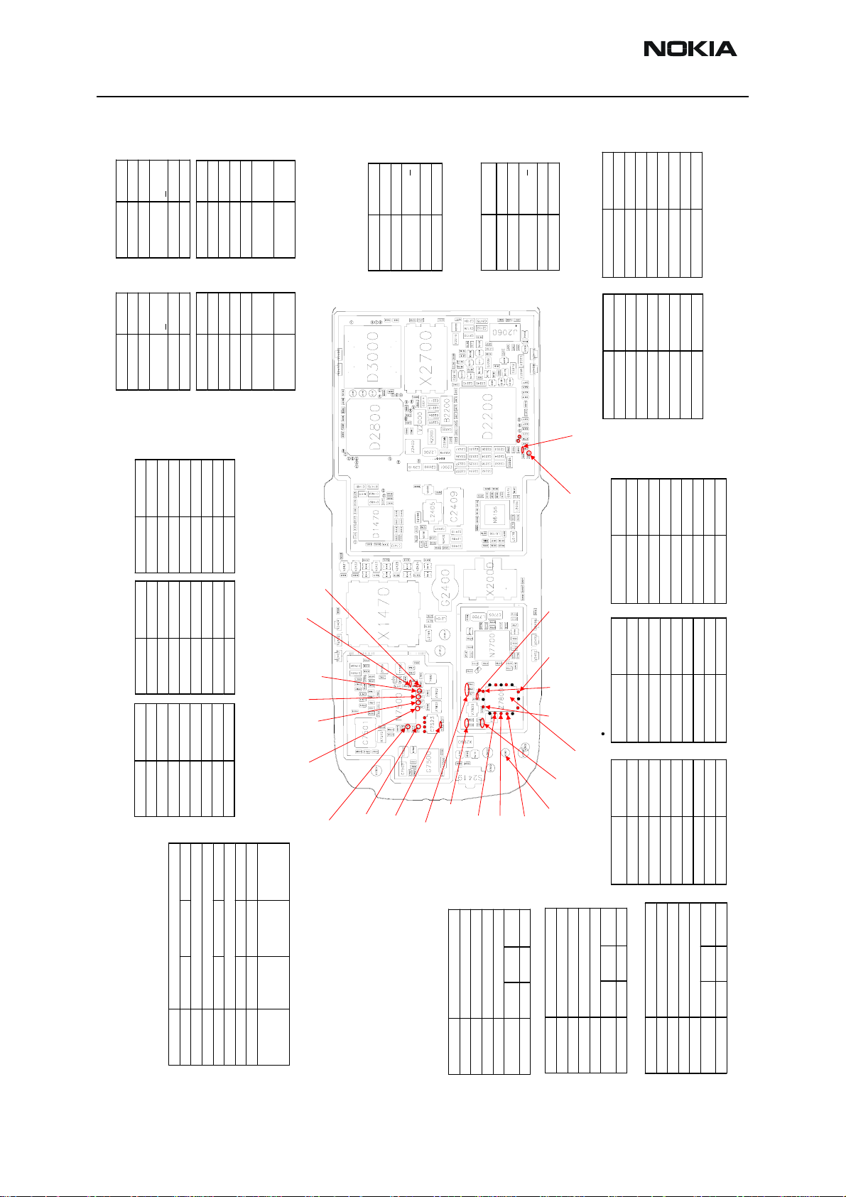
RH-37
Appnedix 6A: Test Points Nokia Customer Care
Receiver test points
B u r s t
V R 6
C o n t i n u o u s
o r
L N A B _ P *
T e s t p o i n t
B a n d G S M 9 0 0
A c t i v e U n i t R X
O p e r a t i o n M o d e
R X / T X C h a n n e l 3 7
D C L e v e l 2 . 8 V
T e s t p o i n t
B a n d G S M 1 9 0 0
A c t i v e U n i t R X
O p e r a t i o n M o d e C o n t i n u o u s
R X / T X C h a n n e l 6 6 1
B u r s t
V R 4
C o n t i n u o u s
T e s t p o i n t
B a n d G S M 9 0 0
A c t i v e U n i t R X
O p e r a t i o n M o d e
R x 3
T e s t p o i n t
B a n d G S M 1 9 0 0
L N A _ P *
o r
T e s t p o i n t
B a n d G S M 1 9 0 0
A c t i v e U n i t R X
O p e r a t i o n M o d e C o n t i n u o u s
R X / T X C h a n n e l 3 7
D C L e v e l 2 . 8 V
A c t i v e U n i t R X
O p e r a t i o n M o d e C o n t i n u o u s
R X / T X C h a n n e l 6 6 1
A G C 1 4
R X / T X C h a n n e l 6 6 1
2 . 5 d B
P r e f
I n p u t P o w e r 6 0 d B m
I n p u t F r e q u e n c y 1 9 6 0 . 0 6 7 7 1 M H z
P r o b e d P o w e r
T y p .
2 . 5 V
A G C : 1 4
D C L e v e l
T y p .
1 . 8 V
0 V
A G C : 4
D C L e v e l
A G C : 5
D C L e v e l
B u r s t
V r e f R F 0 1 *
C o n t i n u o u s o r
T e s t p o i n t
B a n d G S M 9 0 0
A c t i v e U n i t R X
O p e r a t i o n M o d e
R X / T X C h a n n e l 3 7
D C L e v e l 1 . 3 5 V
1 ) V r e f R F 0 2 *
T e s t p o i n t s
B u r s t
C o n t i n u o u s o r
2 ) V r e f R F 0 2 * *
B a n d G S M 9 0 0
A c t i v e U n i t R X
O p e r a t i o n M o d e
R X / T X C h a n n e l 3 7
D C L e v e l 1 . 3 5 V
O U T - Z 7 8 0 1
T e s t p o i n t
B a n d G S M 1 9 0 0
A c t i v e U n i t R X
O p e r a t i o n M o d e C o n t i n u o u s
R X / T X C h a n n e l 6 6 1
O U T - V 7 8 0 0
T e s t p o i n t
B a n d G S M 1 9 0 0
A c t i v e U n i t R X
O p e r a t i o n M o d e C o n t i n u o u s
R X / T X C h a n n e l 6 6 1
V r e f R F 0 2 *
R 2 9 0 1 / C 2 9 0 1
V r e f R F 0 2 * *
R 2 9 0 0 / C 2 9 0 0
1 ) I N P _ P _ R X
2 ) I N M _ P _ R X
P r e f - 3 . 5 d B
A G C 1 4
I n p u t P o w e r 6 0 d B m
I n p u t F r e q u e n c y 1 9 6 0 . 0 6 7 7 1 M H z
P r o b e d P o w e r
P r e f + 1 4 d B
A G C 1 4
I n p u t P o w e r 6 0 d B m
I n p u t F r e q u e n c y 1 9 6 0 . 0 6 7 7 1 M H z
P r o b e d P o w e r
P r e f - 6 . 5 d B
2 . 0 d B
R x 2
T e s t p o i n t
B a n d G S M 1 8 0 0
A c t i v e U n i t R X
O p e r a t i o n M o d e C o n t i n u o u s
R X / T X C h a n n e l 7 0 0
R x 1
T e s t p o i n t
B a n d G S M 8 5 0 / 9 0 0
A c t i v e U n i t R X
O p e r a t i o n M o d e C o n t i n u o u s
R X / T X C h a n n e l 3 7
P r e f
A G C 1 4
I n p u t P o w e r 6 0 d B m
I n p u t F r e q u e n c y 1 8 4 2 . 8 6 7 7 1 M H z
P r o b e d P o w e r
1 . 5 . 0 d B
P r e f
A G C 1 4
I n p u t P o w e r 6 0 d B m
I n p u t F r e q u e n c y 9 4 2 . 4 6 7 7 1 M H z
P r o b e d P o w e r
L a y o u t : 1 c n a _ 4 1 ( B u i l d 4 . 0 )
t y p . 6 3 d B m
P r e f ( d B m )
t y p . 6 3 d B m
P r e f ( d B m )
t y p . 6 3 d B m
A N T ( A n t e n n a F e e d )
R e c e i v e r T e s t P o i n t s ( 1 / 2 )
T e s t p o i n t
B a n d G S M 9 0 0 G S M 1 8 0 0 G S M 1 9 0 0
A c t i v e U n i t R X
O p e r a t i o n M o d e C o n t i n u o u s
R X / T X C h a n n e l 3 7 7 0 0 6 6 1
P r e f ( d B m )
w i t h
A G C 1 4
I n p u t P o w e r 6 0 d B m 6 0 d B m 6 0 d B m
I n p u t F r e q u e n c y 9 4 2 . 4 6 7 7 1 M H z 1 8 4 2 . 8 6 7 7 1 M H z 1 9 6 0 . 0 6 7 7 1 M H z
P r o b e d P o w e r
( e . g . m e a s u r e d
r e s i s t i v e p r o b e , r e f . t o
L 7 8 0 7 / C 7 8 0 6
I N M _ P _ R X
L 7 8 0 7 / C 7 8 0 5
I N P _ P _ R X
L 7 8 0 3
I N P _ D _ R X
L 7 8 0 2
I N M _ D _ R X
L 7 8 0 5
L N A B _ P *
R 7 8 0 1 / C 7 8 0 3
V C 3
V A N T _ 1
V C 1
V A N T _ 2
V C 2
V A N T _ 3
I N M _ G _ R X
L 7 8 0 4
I N P _ G _ R X
L 7 8 0 0 / C 7 8 0 1
O U T - Z 7 8 0 1
V R 6
V R 4
c h a p t e r 5 . 2 )
C 7 5 2 1
C 7 5 1 9
V r e f R F 0 1 *
R 7 5 1 1 / C 7 5 2 4
O U T - V 7 8 0 0
L 7 8 0 1 / C 7 8 0 4 / R 7 8 0 2
R x 3
L N A _ P *
R 7 8 0 0 / C 7 8 0 0
V A N T _ 1 , 2 , 3
T e s t p o i n t
R x 2
( G S M 1 9 0 0 )
( G S M 1 8 0 0 )
( V C 3 )
V A N T _ 3
( V C 1 )
V A N T _ 2
( V C 3 )
V A N T _ 1
B a n d G S M 9 0 0
A c t i v e U n i t R X [ T X ]
O p e r a t i o n M o d e C o n t i n u o u s
R X / T X C h a n n e l 3 7
T e s t p o i n t s
A N T
R x 1
( G S M 8 5 0 / 9 0 0 )
V A N T _ 1 , 2 , 3
T e s t p o i n t
B a n d G S M 1 8 0 0
D C L e v e l 0 V [ 2 . 6 V ] 0 V [ 0 V ] 0 V [ 2 . 6 V ]
A c t i v e U n i t R X [ T X ]
T e s t p o i n t s
B a n d G S M 1 9 0 0
A c t i v e U n i t R X
O p e r a t i o n M o d e C o n t i n u o u s
R X / T X C h a n n e l 6 6 1
A G C 1 4
I n p u t P o w e r 6 0 d B m
I n p u t F r e q u e n c y 1 9 6 0 . 0 6 7 7 1 M H z
P r o b e d P o w e r
D C L e v e l 1 . 6 V
1 ) I N P _ D _ R X
2 ) I N M _ D _ R X
T e s t p o i n t s
B a n d G S M 1 8 0 0
A c t i v e U n i t R X
O p e r a t i o n M o d e C o n t i n u o u s
R X / T X C h a n n e l 7 0 0
G N D
a n d p i n s
( G R O U N D )
m e t a l s h i e l d i n g
1 ) I N P _ G _ R X
2 ) I N M _ G _ R X
T e s t p o i n t s
B a n d G S M 9 0 0
A c t i v e U n i t R X
O p e r a t i o n M o d e C o n t i n u o u s
R X / T X C h a n n e l 3 7
( V C 3 )
V A N T _ 3
( V C 1 )
V A N T _ 2
V A N T _ 1
O p e r a t i o n M o d e C o n t i n u o u s
R X / T X C h a n n e l 7 0 0
T e s t p o i n t s
V A N T _ 1 , 2 , 3
( V C 3 )
D C L e v e l 0 V [ 0 V ] 0 V [ 2 . 6 V ] 0 V [ 2 . 6 V ]
T e s t p o i n t
B a n d G S M 1 9 0 0
P r e f 6 d B
A G C 1 4
I n p u t P o w e r 6 0 d B m
I n p u t F r e q u e n c y 1 8 4 2 . 8 6 7 7 1 M H z
P r o b e d P o w e r
D C L e v e l T y p . 1 . 6 V
P r e f 3 . 5 d B
A G C 1 4
I n p u t P o w e r 6 0 d B m
I n p u t F r e q u e n c y 9 4 2 . 4 6 7 7 1 M H z
P r o b e d P o w e r
D C L e v e l T y p . 1 . 6 V
( V C 3 )
V A N T _ 3
( V C 1 )
V A N T _ 2
( V C 3 )
V A N T _ 1
A c t i v e U n i t R X [ T X ]
O p e r a t i o n M o d e C o n t i n u o u s
R X / T X C h a n n e l 6 6 1
T e s t p o i n t s
D C L e v e l 0 V [ 0 V ] 0 V [ 2 . 6 V ] 2 . 6 V [ 2 . 6 V ]
Page 46 Nokia Corporation Issue 1 07/04
Page 47
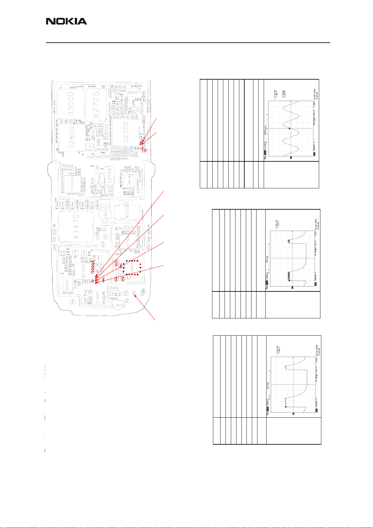
RH-37
R
i
T
P
i
( 2 / 2 )
Nokia Customer Care Appnedix 6A: Test Points
R X I
J 1 0 0 5
R X Q
J 1 0 0 4
1 ) R X I
2 ) R X Q
T e s t p o i n t s
B a n d G S M 9 0 0 o r G S M 1 8 0 0 o r G S M 1 9 0 0
A c t i v e U n i t R X
O p e r a t i o n M o d e C o n t i n u o u s
R X / T X C h a n n e l 3 7 o r 7 0 0 o r 6 6 1
C 7 5 2 3
C M _ D T O S _ I
C 7 5 2 3
C M _ D T O S _ Q
C 7 5 2 3
C M _ F _ I
C 7 5 2 3
C M _ F _ Q
1 ) C M _ F _ I
2 ) C M _ F _ Q
T e s t p o i n t s
B a n d G S M 9 0 0 o r G S M 1 8 0 0 o r G S M 1 9 0 0
A c t i v e U n i t R X
A N T
1 . 4 V p p
A G C 1 0
I n p u t P o w e r 6 0 d B m
I n p u t F r e q u e n c y 9 4 2 . 4 6 7 7 1 , 1 8 4 2 . 8 6 7 7 1 o r 1 9 6 0 . 0 6 7 7 1 M H z
S i g n a l
A m p l i t u d e
D C O f f s e t 1 . 2 8 V d c
F r e q u e n c y 6 7 k H z
G r a p h
( t y p i c a l f o r a l l
T P s a n d b a n d s )
A p p r o x . 1 . 7 5 V p p
O p e r a t i o n M o d e B u r s t
R X / T X C h a n n e l 3 7 o r 7 0 0 o r 6 6 1
A G C 1 0
I n p u t P o w e r 6 0 d B m
I n p u t F r e q u e n c y 9 4 2 . 4 6 7 7 1 , 1 8 4 2 . 8 6 7 7 1 o r 1 9 6 0 . 0 6 7 7 1 M H z
S i g n a l
A m p l i t u d e
G r a p h
( t y p i c a l f o r b o t h
T P s a n d a l l
b a n d s )
n t s
o
1 ) C M _ D T O S _ I
e s t
2 ) C M _ D T O S _ Q
A p p r o x . 2 V p p
v e r
T e s t p o i n t s
B a n d G S M 9 0 0 o r G S M 1 8 0 0 o r G S M 1 9 0 0
A c t i v e U n i t R X
O p e r a t i o n M o d e B u r s t
R X / T X C h a n n e l 3 7 o r 7 0 0 o r 6 6 1
A G C 1 4
I n p u t P o w e r 6 0 d B m
I n p u t F r e q u e n c y 9 4 2 . 4 6 7 7 1 , 1 8 4 2 . 8 6 7 7 1 o r 1 9 6 0 . 0 6 7 7 1 M H z
S i g n a l
A m p l i t u d e
G r a p h
( t y p i c a l f o r b o t h
T P s a n d a l l
b a n d s )
e c e
Issue 1 07/04 Nokia Corporation Page 47
Page 48

RH-37
Appnedix 6A: Test Points Nokia Customer Care
Transmitter test points
VR3
Testpoint
Band GSM900
Active Unit TX
Operation Mode Burst
RX/TX Channel 37
DC Level 2.8V
GMSK ( EDGE = OFF ) 8-PSK ( EDGE = ON )
Burst Burst
Modulation
Band GSM 850 or 90 0 or 1800 or 1900 GSM 850 or 900 or 1800 or 1900
Active Unit TX TX
Operation
Mode
Test point TXC TXC
Graph
e.g.
GSM900 PL10
TXIP (R713/1)
TXIM (R713/3)
TXIP (R713/7)
TXQM (R713/5))
Testpoints
Band GSM 850 or 900 or GSM1800 or GSM1900
Active Unit TX
Operation Mode Burst
RX/TX Channel 190 or 37 or 700 o r 661
Tx Data Type Random
Tx Power Level any
Tx2
Tx1
Rx3
Transmitter Test Points (1/3)
Rx2
Rx1
_1
VANT
Test points: RFout_900 and RFout_1800/1900
Matrix Antenna Switch Module Z7800
_3
VANT
_2
VANT
RFout
RFout
520mVpp
Signal
Amplitude
/1900
_1800
_900
VC3
VC2
VC1
[Volt]
Test point VTXB_900 VTXB_900
Graph e.g.
GSM900 PL10
Test point VPctrl_9 00 VPctrl_900
Graph
e.g.
GSM900 PL10
Test point VDET
VREF01
Testpoint
Band GSM900
Active Unit TX
Operation Mode Burst
RX/TX Channel 37
DC Level 1.35V
Layout: 1cna_41 (Build 4.0)
TXA
VPCTRL_1800_1900
VBAT
DC Offset 1.2Vdc
Graph
(typical for all
TPs and bands)
Tx
1800
GSM
/1900
Tx
850
/900
GSM
Rx
1900
GSM
X
Rx
1800
GSM
Rx
850
/900
GSM
[Volt]
[Volt]
0 0 0 X
0 0 0
VR2 (C7512)
X
X
X
Testpoint
Band GSM900/1800/1900
VBAT
0 2.6 2.6
0 2.6 0
2.6 2.6 0
Testpoint
Band GSM900
Active Unit TX
Active Unit TX
Operation Mode Burst
RX/TX Channel 37
DC Level 2.8V
Operation Mode Burst
RX/TX Channel 37
DC Level Typ. 3.6V
RFin_1800_1900
VTXB_1800_1900
VTXB_900
VR3
RFin_900 P
RFin_1800_1900 P
TXC
RFin_900 M
RFin_1800_1900 M
VR2
TXQP
TXQM
(C7530)
TXIP
TXIM
(C7529)
VrefRF01*
VPCTRL_900
RFin_900
MODE
Iref_900
Iref_1800_1900 DETRFout_900
RFout_1800_1900
ANT
Page 48 Nokia Corporation Issue 1 07/04
Page 49

RH-37
Nokia Customer Care Appnedix 6A: Test Points
+ 2 d B m
+ d B m
1 . R F i n _ 9 0 0 P
2 . R F i n _ 9 0 0 M
T e s t p o i n t
B a n d G S M 8 5 0 o r 9 0 0
A c t i v e U n i t T X
O p e r a t i o n M o d e B u r s t
M o d u l a t i o n G M S K ( E d g e = o f f )
R X / T X C h a n n e l 1 9 0 o r 3 7
T x P o w e r L e v e l 1 0
T x D a t a T y p e A l l 1
P o w e r @ 5 0 O h m s
P o w e r @ p r o b e
+ 2 d B m
+ d B m
R F i n _ 9 0 0
1 . R F i n _ 1 8 0 0 _ 1 9 0 0 P
2 . R F i n _ 1 8 0 0 _ 1 9 0 0 M
T e s t p o i n t
B a n d G S M 1 8 0 0 o r 1 9 0 0
A c t i v e U n i t T X
O p e r a t i o n M o d e B u r s t
M o d u l a t i o n G M S K ( E d g e = o f f )
R F i n _ 1 8 0 0 _ 1 9 0 0
L a y o u t : 1 c n a _ 4 1 ( B u i l d 4 . 0 )
V P C T R L _ 1 8 0 0 _ 1 9 0 0
T X A
T e s t p o i n t
B a n d G S M 8 5 0 o r 9 0 0
A c t i v e U n i t T X
O p e r a t i o n M o d e B u r s t
M o d u l a t i o n G M S K ( E d g e = o f f )
R X / T X C h a n n e l 1 9 0 o r 3 7
T x P o w e r L e v e l 1 0
T x D a t a T y p e A l l 1
P o w e r @ 5 0 O h m s
P o w e r @ p r o b e
T e s t p o i n t
B a n d G S M 1 8 0 0 o r 1 9 0 0
A c t i v e U n i t T X
O p e r a t i o n M o d e B u r s t
M o d u l a t i o n G M S K ( E d g e = o f f )
V B A T
V P C T R L _ 9 0 0
+ 0 d B m
R X / T X C h a n n e l 7 0 0 o r 6 6 1
T x P o w e r L e v e l 5
T x D a t a T y p e A l l 1
P o w e r @ 5 0 O h m s
+ 2 d B m
R X / T X C h a n n e l 7 0 0 o r 6 6 1
T x P o w e r L e v e l 5
T x D a t a T y p e A l l 1
P o w e r @ 5 0 O h m s
+ d B m
P o w e r @ p r o b e
+ d B m
P o w e r @ p r o b e
R F i n _ 1 8 0 0 _ 1 9 0 0
+ d B m
R F o u t _ 9 0 0
+ 2 4 . 3 d B m
R F i n _ 9 0 0
R F o u t _ 1 8 0 0 _ 1 9 0 0
M O D E
I r e f _ 9 0 0
+ d B m
+ 2 1 . 6 d B m
V T X B _ 1 8 0 0 _ 1 9 0 0
T e s t p o i n t
B a n d G S M 8 5 0 o r 9 0 0
A c t i v e U n i t T X
O p e r a t i o n M o d e B u r s t
M o d u l a t i o n G M S K ( E d g e = o f f )
R X / T X C h a n n e l 1 9 0 o r 3 7
T x P o w e r L e v e l 1 0
T x D a t a T y p e A l l 1
P o w e r @ 5 0 O h m s
P o w e r @ p r o b e
V T X B _ 9 0 0
T X C
T e s t p o i n t
B a n d G S M 1 8 0 0 o r 1 9 0 0
A c t i v e U n i t T X
O p e r a t i o n M o d e B u r s t
M o d u l a t i o n G M S K ( E d g e = o f f )
R X / T X C h a n n e l 7 0 0 o r 6 6 1
T x P o w e r L e v e l 5
T x D a t a T y p e A l l 1
P o w e r @ 5 0 O h m s
P o w e r @ p r o b e
I r e f _ 1 8 0 0 _ 1 9 0 0 D E TR F o u t _ 9 0 0
V R 3
+ 2 0 d B m
+ 2 3 d B m
+ d B m
R F i n _ 9 0 0 P
A N T
R F i n _ 9 0 0 M
A N T
+ d B m
R F o u t _ 1 8 0 0 _ 1 9 0 0
T e s t p o i n t
B a n d G S M 8 5 0 o r 9 0 0
A c t i v e U n i t T X
O p e r a t i o n M o d e B u r s t
M o d u l a t i o n G M S K ( E d g e = o f f )
R X / T X C h a n n e l 1 9 0 o r 3 7
T x P o w e r L e v e l 1 0
T x D a t a T y p e A l l 1
P o w e r @ 5 0 O h m s
P o w e r @ p r o b e
V R 2
T X Q P
T X Q M
R F i n _ 1 8 0 0 _ 1 9 0 0 P
R F i n _ 1 8 0 0 _ 1 9 0 0 M
( C 7 5 3 0 )
T X I P
T X I M
( C 7 5 2 9 )
V r e f R F 0 1 *
A N T
T e s t p o i n t
B a n d G S M 1 8 0 0 o r 1 9 0 0
A c t i v e U n i t T X
O p e r a t i o n M o d e B u r s t
M o d u l a t i o n G M S K ( E d g e = o f f )
R X / T X C h a n n e l 7 0 0 o r 6 6 1
T x P o w e r L e v e l 5
T x D a t a T y p e A l l 1
P o w e r @ 5 0 O h m s
P o w e r @ p r o b e
R F @ T e s t - J i g
T e s t p o i n t
B a n d G S M 8 5 0 o r 9 0 0
A c t i v e U n i t T X
O p e r a t i o n M o d e B u r s t
m e a s u r e m e n t w i t h t h e 5 0 O h m s p o w e r m e a s u r e m e n t .
P o w e r m e a s u r e m e n t s a t t h e t e s t p o i n t s b y m e a n s o f a p r o b e w i t h 4 7 0 ( ! ) O h m s a t t h e p e a k o n l y . G a i n s o r l o s s e s o f t h e k e y c o m p o n e n t s d e t e c t e d w i t h t h e p r o b e s h a l l b e c o m p a r a b l e t o t h e
M o d u l a t i o n G M S K ( E d g e = o f f )
T y p . + 2 3 d B m
R X / T X C h a n n e l 1 9 0 o r 3 7
T x P o w e r L e v e l 1 0
T x D a t a T y p e A l l 1
P o w e r @ 5 0 O h m
L o s s e s o f j i g c o m p e n s a t e d
R F @ T e s t - J i g
T e s t p o i n t
B a n d G S M 1 8 0 0 o r 1 9 0 0
A c t i v e U n i t T X
O p e r a t i o n M o d e B u r s t
M o d u l a t i o n G M S K ( E d g e = o f f )
T y p . + 2 0 d B m
R X / T X C h a n n e l 7 0 0 o r 6 6 1
T x P o w e r L e v e l 5
T x D a t a T y p e A l l 1
P o w e r @ 5 0 O h m s
Issue 1 07/04 Nokia Corporation Page 49
L o s s e s o f j i g c o m p e n s a t e d
Page 50
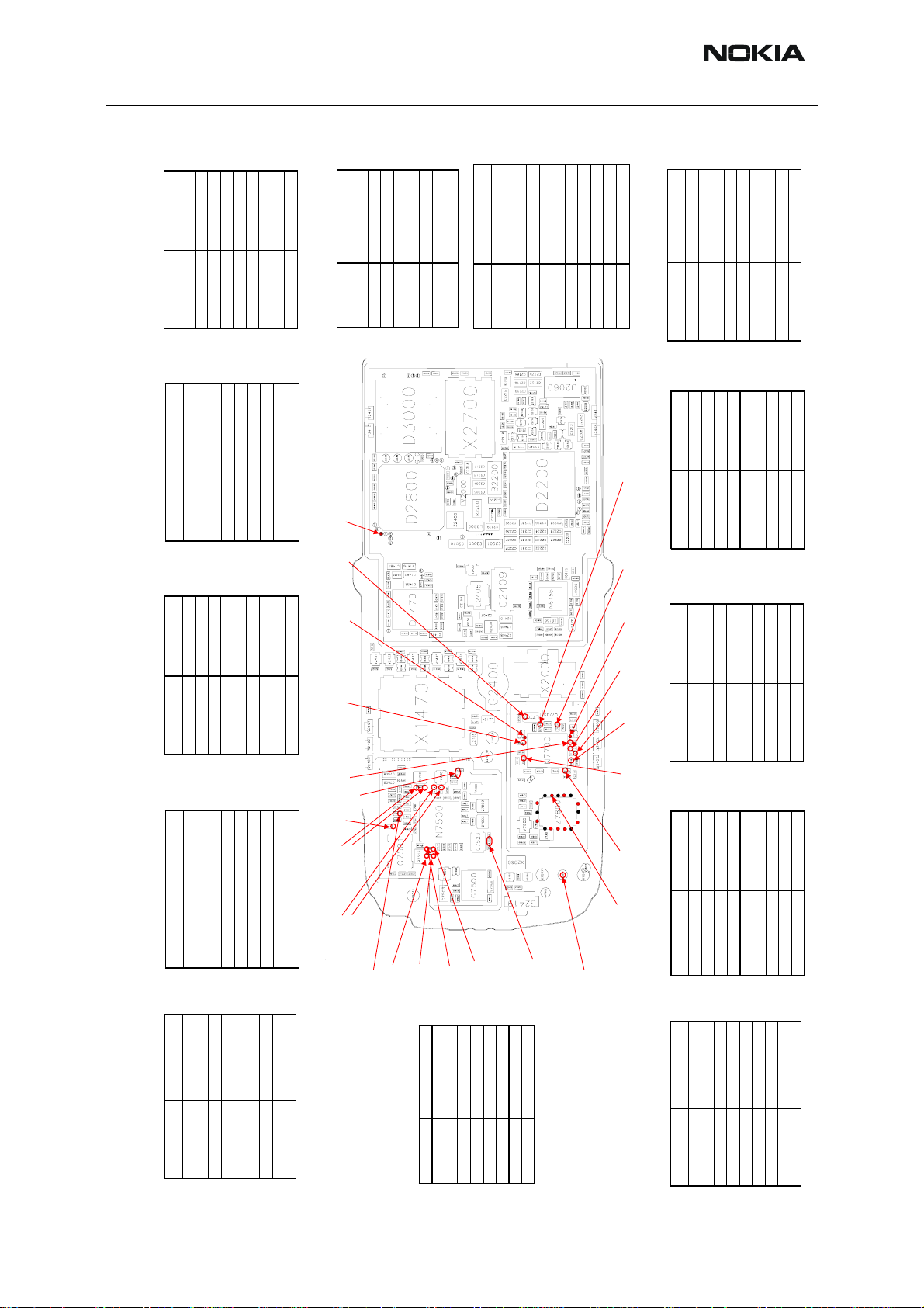
RH-37
Appnedix 6A: Test Points Nokia Customer Care
- 1 5 - 8 d B m
1 . R F i n _ 9 0 0 P
2 . R F i n _ 9 0 0 M
T e s t p o i n t
B a n d G S M 8 5 0 o r 9 0 0
A c t i v e U n i t T X
O p e r a t i o n M o d e B u r s t
M o d u l a t i o n 8 - P S K ( E d g e = o n )
R X / T X C h a n n e l 1 9 0 o r 3 7
R F i n _ 9 0 0
T e s t p o i n t
B a n d G S M 8 5 0 o r 9 0 0
A c t i v e U n i t T X
O p e r a t i o n M o d e B u r s t
M o d u l a t i o n 8 - P S K ( E d g e = o n )
R X / T X C h a n n e l 1 9 0 o r 3 7
d B m
1 . R F i n _ 1 8 0 0 _ 1 9 0 0 P
B O M 1 , B O M 2 , B O M 2 b
I r e f _ 9 0 0
T x P o w e r L e v e l 1 0
T x D a t a T y p e A l l 1
P o w e r @ 5 0 O h m s
P o w e r @ p r o b e
d B m
- 1 5 - 8 d B m
G S M 8 5 0 o r 9 0 0
T e s t p o i n t
B a n d
A c t i v e U n i t T X
O p e r a t i o n M o d e B u r s t
M o d u l a t i o n 8 - P S K ( E d g e = o n )
R X / T X C h a n n e l 1 9 0 o r 3 7
T x P o w e r L e v e l 1 0
T x D a t a T y p e A l l 1
U s e s a m e t e s t p o i n t
I r e f _ 9 0 0 f o r h i g h e r G S M
I r e f _ 1 8 0 0 _ 1 9 0 0 ( B O M 1 )
I r e f _ 9 0 0 ( B O M 2 , B O M 2 b )
b a n d s i n c a s e o f B O M 2
a n d B O M 2 b !
G S M 1 8 0 0 o r 1 9 0 0
V o l t a g e 1 . 9 2 V ( B u r s t )
T e s t p o i n t
R E M A R K
B a n d
A c t i v e U n i t T X
O p e r a t i o n M o d e B u r s t
M o d u l a t i o n 8 - P S K ( E d g e = o n )
R X / T X C h a n n e l 7 0 0 o r 6 6 1
T x P o w e r L e v e l 1 0
T x D a t a T y p e A l l 1
V o l t a g e 2 . 0 V ( B u r s t )
2 . R F i n _ 1 8 0 0 _ 1 9 0 0 M
T e s t p o i n t
B a n d G S M 1 8 0 0 o r 1 9 0 0
A c t i v e U n i t T X
O p e r a t i o n M o d e B u r s t
M o d u l a t i o n 8 - P S K ( E d g e = o n )
R F i n _ 1 8 0 0 _ 1 9 0 0
- 1 8 - 1 0 d B m
R X / T X C h a n n e l 7 0 0 o r 6 6 1
T x P o w e r L e v e l 5
T x D a t a T y p e A l l 1
P o w e r @ 5 0 O h m s
- 1 6 - 8 d B m
L a y o u t : 1 c n a _ 4 1 ( B u i l d 4 . 0 )
V P C T R L _ 1 8 0 0 _ 1 9 0 0
T x P o w e r L e v e l 1 0
T x D a t a T y p e A l l 1
P o w e r @ 5 0 O h m s
P o w e r @ p r o b e
T X A
T e s t p o i n t
B a n d G S M 1 8 0 0 o r 1 9 0 0
A c t i v e U n i t T X
O p e r a t i o n M o d e B u r s t
M o d u l a t i o n 8 - P S K ( E d g e = o n )
R X / T X C h a n n e l 7 0 0 o r 6 6 1
T x P o w e r L e v e l 5
T x D a t a T y p e A l l 1
P o w e r @ 5 0 O h m s
d B m
P o w e r @ p r o b e
d B m
P o w e r @ p r o b e
V B A T
V P C T R L _ 9 0 0
+ 2 5 . 8 d B m
R F o u t _ 9 0 0
T e s t p o i n t
B a n d G S M 8 5 0 o r 9 0 0
A c t i v e U n i t T X
O p e r a t i o n M o d e B u r s t
M o d u l a t i o n 8 - P S K ( E d g e = o n )
R X / T X C h a n n e l 1 9 0 o r 3 7
+ d B m
T x P o w e r L e v e l 1 0
T x D a t a T y p e A l l 1
P o w e r @ 5 0 O h m s
P o w e r @ p r o b e
R F i n _ 1 8 0 0 _ 1 9 0 0
V T X B _ 1 8 0 0 _ 1 9 0 0
V T X B _ 9 0 0
T X C
V R 3
+ 2 4 . 5 d B m
A N T
T e s t p o i n t
B a n d G S M 8 5 0 o r 9 0 0
A c t i v e U n i t T X
O p e r a t i o n M o d e B u r s t
M o d u l a t i o n 8 - P S K ( E d g e = o n )
R X / T X C h a n n e l 1 9 0 o r 3 7
+ d B m
R F i n _ 9 0 0 P
T x P o w e r L e v e l 1 0
T x D a t a T y p e A l l 1
P o w e r @ 5 0 O h m s
P o w e r @ p r o b e
R F i n _ 9 0 0 M
V R 2
T X Q P
T X Q M
R F i n _ 1 8 0 0 _ 1 9 0 0 P
R F i n _ 1 8 0 0 _ 1 9 0 0 M
( C 7 5 3 0 )
T X I P
T X I M
( C 7 5 2 9 )
V r e f R F 0 1 *
R F i n _ 9 0 0
+ 2 3 . 1 d B m
R F o u t _ 1 8 0 0 _ 1 9 0 0
M O D E
I r e f _ 9 0 0
T e s t p o i n t
B a n d G S M 1 8 0 0 o r 1 9 0 0
A c t i v e U n i t T X
O p e r a t i o n M o d e B u r s t
M o d u l a t i o n 8 - P S K ( E d g e = o n )
R X / T X C h a n n e l 7 0 0 o r 6 6 1
+ d B m
T x P o w e r L e v e l 5
T x D a t a T y p e A l l 1
P o w e r @ 5 0 O h m s
P o w e r @ p r o b e
I r e f _ 1 8 0 0 _ 1 9 0 0 D E TR F o u t _ 9 0 0
+ d B m
A N T
R F o u t _ 1 8 0 0 _ 1 9 0 0
T e s t p o i n t
B a n d G S M 1 8 0 0 o r 1 9 0 0
A c t i v e U n i t T X
O p e r a t i o n M o d e B u r s t
M o d u l a t i o n 8 - P S K ( E d g e = o n )
+ 2 1 . 5 d B m
R X / T X C h a n n e l 7 0 0 o r 6 6 1
T x P o w e r L e v e l 5
T x D a t a T y p e A l l 1
P o w e r @ 5 0 O h m s
P o w e r @ p r o b e
A N T
R F @ T e s t - J i g
T e s t p o i n t
B a n d G S M 8 5 0 o r 9 0 0
A c t i v e U n i t T X
O p e r a t i o n M o d e B u r s t
m e a s u r e m e n t w i t h t h e 5 0 O h m s p o w e r m e a s u r e m e n t .
P o w e r m e a s u r e m e n t s a t t h e t e s t p o i n t s b y m e a n s o f a p r o b e w i t h 4 7 0 ( ! ) O h m s a t t h e p e a k o n l y . G a i n s o r l o s s e s o f t h e k e y c o m p o n e n t s d e t e c t e d w i t h t h e p r o b e s h a l l b e c o m p a r a b l e t o t h e
M o d u l a t i o n 8 - P S K ( E d g e = o n )
T y p . + 2 4 . 5 d B m
M O D E
R X / T X C h a n n e l 1 9 0 o r 3 7
T x P o w e r L e v e l 1 0
T x D a t a T y p e A l l 1
P o w e r @ 5 0 O h m s
L o s s e s o f j i g c o m p e n s a t e d
T e s t p o i n t
B a n d G S M 8 5 0 / 9 0 0 / 1 8 0 0 / 1 9 0 0
A c t i v e U n i t T X
O p e r a t i o n M o d e B u r s t
M o d u l a t i o n 8 - P S K ( E d g e = o n )
R X / T X C h a n n e l 1 9 0 o r 3 7 o r 7 0 0 o r 6 6 1
T x P o w e r L e v e l 1 0
T x D a t a T y p e A l l 1
V o l t a g e 1 . 9 6 V ( B u r s t )
R F @ T e s t - J i g
T e s t p o i n t
B a n d G S M 1 8 0 0 o r 1 9 0 0
A c t i v e U n i t T X
O p e r a t i o n M o d e B u r s t
M o d u l a t i o n 8 - P S K ( E d g e = o n )
+ 2 1 . 5 d B m
R X / T X C h a n n e l 7 0 0 o r 6 6 1
T x P o w e r L e v e l 5
T x D a t a T y p e A l l 1
P o w e r @ 5 0 O h m s
L o s s e s o f j i g c o m p e n s a t e d
Page 50 Nokia Corporation Issue 1 07/04
Page 51

RH-37
Nokia Customer Care Appnedix 6A: Test Points
Synthesizer test points
M e a s u r e d u s i n g t h e s p e c i a l p r o b e w i t h
~ 0 d B m ~ 0 d B m ~ 0 d B m
c a p a c i t i v e c o u p l i n g . N o e x a c t p o w e r
T a k e c a r e t o s e l e c t t h e h i g h e s t P C L 1 5 i f
a c t i v a t i n g T X C o n t i n u o u s m o d e , o t h e r w i s e
t h e p o w e r a m p l i f i e r w i l l b e d e s t r o y e d .
T e s t p o i n t A F C ( V c o f V C T C X O )
B a n d d e f a u l t
A c t i v e U n i t R X
O p e r a t i o n M o d e C o n t i n u o u s
R X / T X C h a n n e l a n y
A F C ( v a l u e ) - 1 0 2 4 1 5 0 1 0 2 3
A F C v o l t a g e 0 . 1 V 1 . 4 V 2 . 5 V
T e s t p o i n t V c o f V C O
B a n d G S M 1 8 0 0 G S M 1 9 0 0 G S M 1 9 0 0
A c t i v e U n i t T X T X R X
O p e r a t i o n M o d e C o n t i n u o u s
R X / T X C h a n n e l 5 1 2 5 1 2 8 1 0
F r e q u e n c y 3 4 2 0 . 4 M H z 3 7 0 0 . 4 M H z 3 9 7 9 . 6 M H z
D C L e v e l ~ 1 . 3 V ~ 2 . 5 V ~ 3 . 6 V
T e s t p o i n t V R 1 V r e f R F 0 1 V r e f R F 0 2
B a n d d e f a u l t ( G S M 9 0 0 o r G S M 8 5 0 )
A c t i v e U n i t R x
O p e r a t i o n M o d e B u r s t o r C o n t i n u o u s
R X / T X C h a n n e l d e f a u l t
D C L e v e l 4 . 7 6 1 . 3 5 V 1 . 3 5 V
T e s t p o i n t V R 3 V R 5 V R 7
B a n d d e f a u l t ( G S M 9 0 0 o r G S M 8 5 0 )
A c t i v e U n i t R x
O p e r a t i o n M o d e B u r s t o r C o n t i n u o u s
R X / T X C h a n n e l d e f a u l t
D C L e v e l 2 . 7 8 V 2 . 7 8 V 2 . 7 8 V
R F B u s C l k , R F B u s D a t a , R F B u s E n a 1
~ 2 V
N o t e
( C 2 9 0 2 / R 2 9 0 2 )
R F C L K _ I
T e s t p o i n t V C O o u t
B a n d G S M 1 8 0 0 G S M 1 9 0 0 G S M 1 9 0 0
A c t i v e U n i t T X T X R X
O p e r a t i o n M o d e C o n t i n u o u s
R X / T X C h a n n e l 5 1 2 5 1 2 8 1 0
F r e q u e n c y 3 4 2 0 . 4 M H z 3 7 0 0 . 4 M H z 3 9 7 9 . 6 M H z
L e v e l
m e a s u r e m e n t p o s s i b l e .
( s p e c . r a n g e =
N o t e s
- 3 . 5 + 2 . 5 d B m )
T a k e c a r e t o s e l e c t t h e h i g h e s t P C L 1 5 i f
a c t i v a t i n g T X C o n t i n u o u s m o d e , o t h e r w i s e
t h e p o w e r a m p l i f i e r w i l l b e d e s t r o y e d .
R F B u s C l k ( J 1 0 0 1 )
T e s t p o i n t
B a n d d e f a u l t ( G S M 9 0 0 o r G S M 8 5 0 )
A c t i v e U n i t R X
O p e r a t i o n M o d e B u r s t
R X / T X C h a n n e l d e f a u l t
S i g n a l
A m p l i t u d e
G r a p h
R F B u s C l k
R F B u s D a t a R F B u s E n a 1
R F B u s D a t a ( J 1 0 0 3 )
R F B u s E n a 1 ( J 1 0 0 2 )
V R 1 V R 5
V R 3
2 6 M H z
V C T C X O o u t
L a y o u t : 1 c n a _ 4 1 ( B u i l d 4 . 0 )
V C T C X O o u t ( R E F C L K )
T e s t p o i n t
B a n d d e f a u l t
S y n t h e s i z e r T e s t P o i n t s ( 1 / 1 )
8 8 0 m V p p
A c t i v e U n i t R X
O p e r a t i o n M o d e C o n t i n u o u s
R X / T X C h a n n e l d e f a u l t
S i g n a l
A m p l i t u d e
D C O f f s e t 1 . 5 V
F r e q u e n c y 2 6 M H z
G r a p h
m e a s u r e d w i t h p a s s i v e p r o b e 1 0 x , 1 0 M o h m / 8 p F , A C c o u p l e d )
A F C ( G 7 5 0 1 )
V c o f V C T C X O
V c o f V C O
( C 7 5 0 3 )
V C O o u t
3 . . 4 . 5 G H z
V r e f R F 0 1
V R 7 ( C 7 5 0 0 )
Issue 1 07/04 Nokia Corporation Page 51
Page 52

RH-37
Appnedix 6A: Test Points Nokia Customer Care
[This page left intentionally blank]
Page 52 Nokia Corporation Issue 1 07/04
 Loading...