

Page 1

Programmes After Market Services
NHE–8/9 Series Transceivers
Disassembly &
Troubleshooting
issue 3 12/98
Page 2

NHE–8/9
PAMS
Disassembly & Troubleshooting
Technical Documentation
CONTENTS
Disassembly 3. . . . . . . . . . . . . . . . . . . . . . . . . . . . . . . . . . . . . . . . . . . . . . . . . . . . .
Troubleshooting 4. . . . . . . . . . . . . . . . . . . . . . . . . . . . . . . . . . . . . . . . . . . . . . . . . .
General 4. . . . . . . . . . . . . . . . . . . . . . . . . . . . . . . . . . . . . . . . . . . . . . . . . . . . . .
System Module Troubleshooting 4. . . . . . . . . . . . . . . . . . . . . . . . . . . . . . . .
Phone is totally dead 5. . . . . . . . . . . . . . . . . . . . . . . . . . . . . . . . . . . . . . . . . .
Flash programming doesn‘t work 6. . . . . . . . . . . . . . . . . . . . . . . . . . . . . . . .
Power doesn‘t stay on or the phone is jammed 9. . . . . . . . . . . . . . . . . . . .
Display information: Contact service 11. . . . . . . . . . . . . . . . . . . . . . . . . . . . .
Phone doesn‘t register (no serv) or doesn‘t make a call 12. . . . . . . . . . . .
SIM Card is out of order (insert SIM card or card rejected) 14. . . . . . . . . .
Audio fault 17. . . . . . . . . . . . . . . . . . . . . . . . . . . . . . . . . . . . . . . . . . . . . . . . . . . .
Charging fault 19. . . . . . . . . . . . . . . . . . . . . . . . . . . . . . . . . . . . . . . . . . . . . . . . .
UIF Module troubleshooting 20. . . . . . . . . . . . . . . . . . . . . . . . . . . . . . . . . . . . . . .
UIF– connector 20. . . . . . . . . . . . . . . . . . . . . . . . . . . . . . . . . . . . . . . . . . . . . . .
LCD 20. . . . . . . . . . . . . . . . . . . . . . . . . . . . . . . . . . . . . . . . . . . . . . . . . . . . . . . . .
Microphone 20. . . . . . . . . . . . . . . . . . . . . . . . . . . . . . . . . . . . . . . . . . . . . . . . . . .
Earpiece 20. . . . . . . . . . . . . . . . . . . . . . . . . . . . . . . . . . . . . . . . . . . . . . . . . . . . .
Buzzer 20. . . . . . . . . . . . . . . . . . . . . . . . . . . . . . . . . . . . . . . . . . . . . . . . . . . . . . .
Keyboard and display LEDs 21. . . . . . . . . . . . . . . . . . . . . . . . . . . . . . . . . . . .
Page 2
issue 3 12/98
Page 3
PAMS
NHE–8/9
Technical Documentation
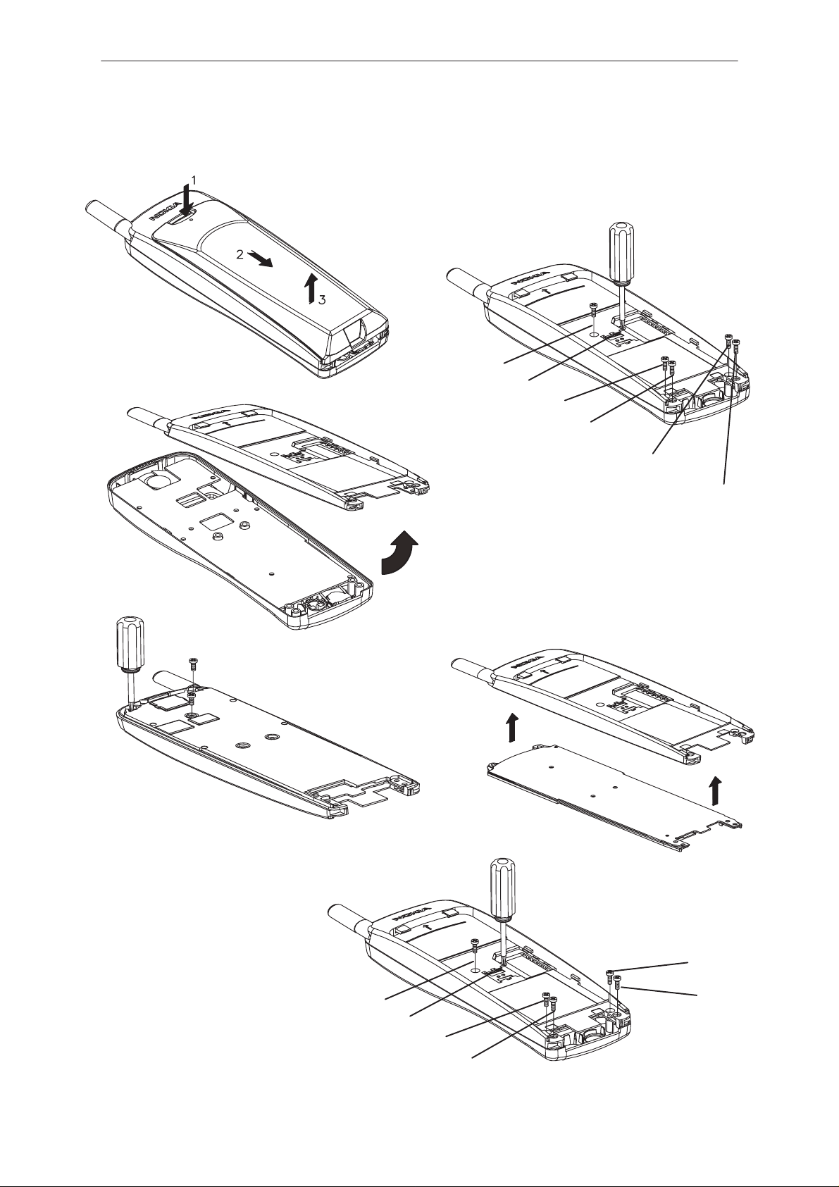
Disassembly
Remove battery
1
Disassembly & Troubleshooting
Remove 6 screws from the
2
chassis. Use the numbered
order.
2
1
3
4
5
4
Remove 3 screws from the shield
3
Remove the B cover beginning
from the bottom of the phone. Be
careful not to damage the board
to board connector!
5
Remove the shield
6
6
Re–assemble the phone in
reverse order. Note! Use the
numbered order when assembling the 6 screws and
tighten them to a torque of
0.15 Nm.
issue 3 12/98
1
5
3
6
2
4
Page 3
Page 4

NHE–8/9
PAMS
Disassembly & Troubleshooting
Troubleshooting
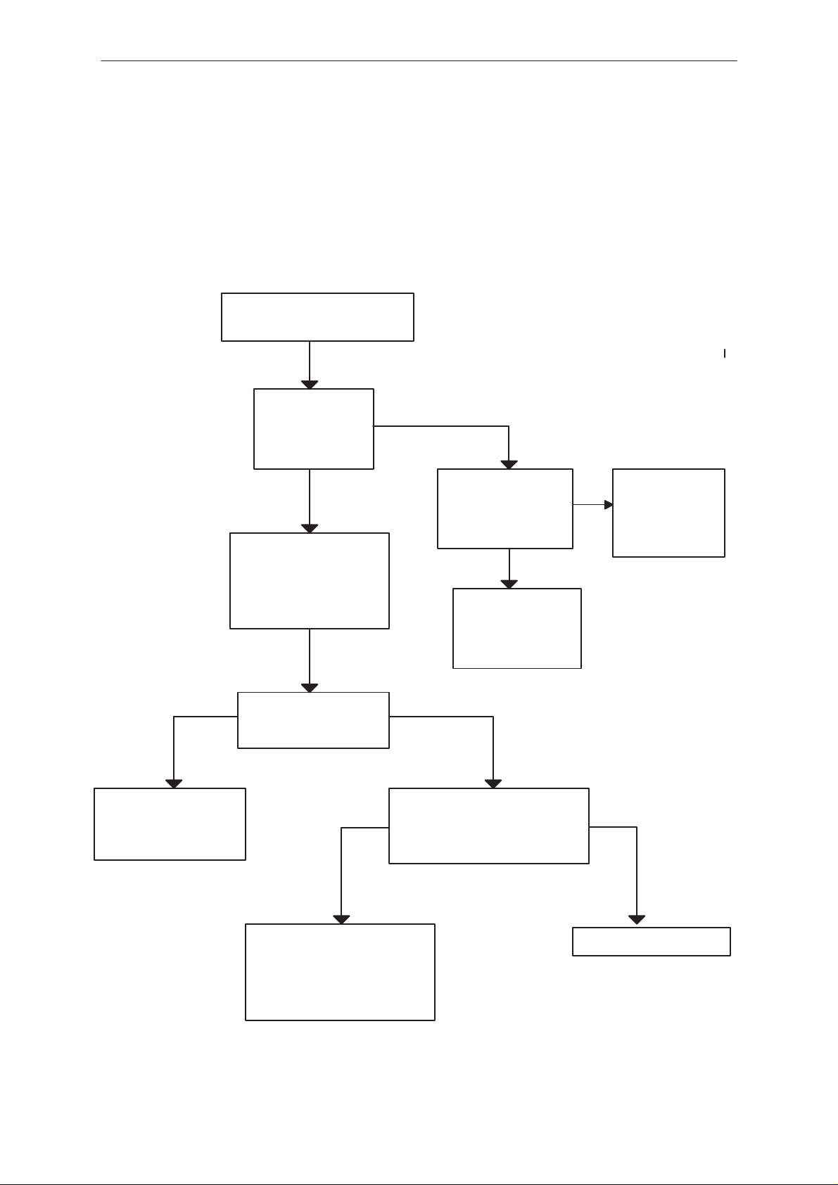
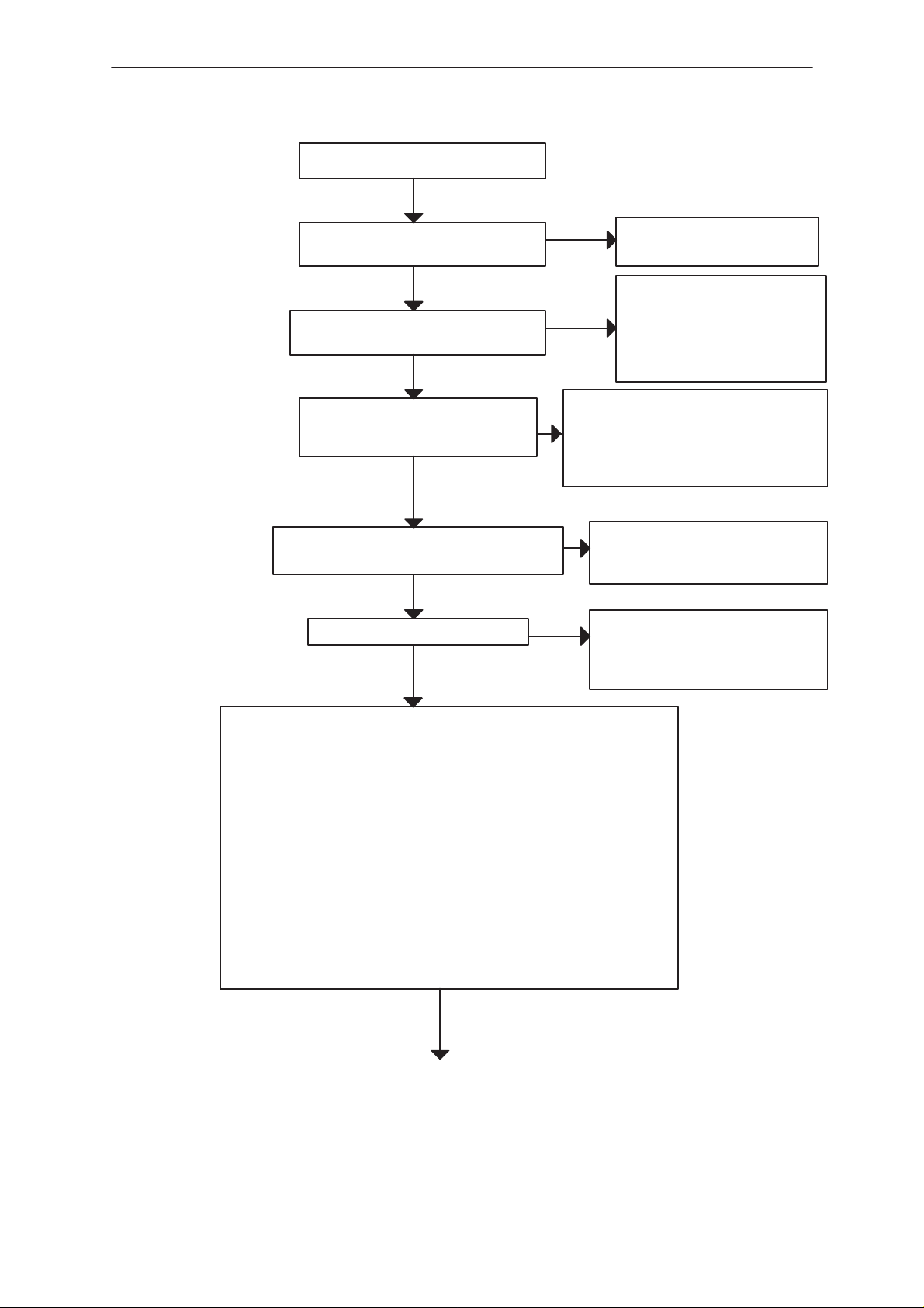
General
The purpose is to define the faulty module block, and then to locate the
faulty component. The trouble shooting diagram has been planned so that
the fault, whatever it is, can be found by as simple measurements as
possible.
The flow charts give you the overview of the blocks. The purpose is that
you proceed through the flow diagram so that, if your answer is YES for
the asked question, go straight to the next level, but if your answer is NO,
you have to go the sub–branch.
Required servicing equipment:
– PC for Service Software
– Power supply (2.0 A)
– Digital multimeter
Technical Documentation
– Oscilloscope
– Spectrum analyzer
– Signal generator
– RF cables
– Modular cable
– RS232/MBUS adapter
– HP8922H or equivalent
– RF measuring chassis
System Module Troubleshooting
The following hints should facilitate finding the cause of the problem when
the circuitry seems to be faulty. This trouble shooting guide is divided into
the following sections.
1. Phone is totally dead
2. Flash programming doesn‘t work
3. Power doesn‘t stay on or the phone is jammed
4. Display information: Contact Service
5. Phone doesn‘t register to the network or phone doesn‘t make a call.
6. Plug in SIM card is out of order (insert SIM card or card rejected).
7. Audio fault.
Page 4
The first thing to do is carry out a thorough visual check of the module.
Ensure in particular that:
a) there is not any mechanical damage
b) soldered joints are OK
issue 3 12/98
Page 5
PAMS
NHE–8/9
Technical Documentation
Phone is totally dead
Trouble shooting diagram for this fault is represented in figure below
Check at first that the battery back is OK and it is not empty.
This kind of fault has been limited around the system connector (X100)
and the PSCLD (N300).
If the phone is totally dead,
check that
Voltage level at
PSCLD (N300)
pin 25 is same
as VBA T
Connect pins 18, 22
and 31 together (X101)
and measure that voltage level at pin 25
(N300)drop to zero.
YES
NO
Disassembly & Troubleshooting
PSCLD N300
pins 5,21,37 voltage level is
same as VBAT
NO
Check coils L311 +
L301 and the sol–
dered joints of the
connector X100
Rise up PSCLD
pin 25.
YES
If the DC voltage
is still missing
change N300
NO
Check soldered joints
of X100 and PCB
wires between X100
and N300
The voltage level at
pin 25 (N300) is zero
PSCLD (N300) switches
power on so the regulated
voltages VL, VA and VSL are
3.16V
Check that capacitors C329,
C330, C310 and C311 are
soldered. Check also soldered joints of N300. If these
things are correct, change
N300
YES
YESNO
Check the UI board and
the PWR button.
issue 3 12/98
Page 5
Page 6

NHE–8/9
PAMS
Disassembly & Troubleshooting
Flash programming doesn‘t work
In error cases, the flash prommer can give some information about a
fault.
The fault information messages could be:
– MCU doesn‘t boot
– MCU flash Vpp error
– Serial data line failure
– Serial clock line failure
– External RAM fault
– Algorithm file or alias ID don‘t find
In cases that the the flash programming doesn‘t succeed, there is a
possibility to test the interface between the ASIC and the MCU.
This test is useful to do, when the fault information is: MCU doesn‘t boot
or Serial clock line failure.
Technical Documentation
The test procedure is following:
1. Connect a short circuit wire between Asic pins 137 and gnd.
2. Switch power on.
3. If the reset line of the MCU rises up, the interface is OK. Otherwise the
reset line stays low.
Note: this test can only find short circuits, not open pins.
Page 6
issue 3 12/98
Page 7
PAMS
NHE–8/9
Technical Documentation
Output voltages of PSCLD (N300)
are 3.16 V ( VL, VA, VSL )
Master Reset (Purx), PSCLD pin 26
is ”1” ( 3.16 V )
Clock signal at the input of MCU (D150),
pin 51 is 6.5 MHz square wave.
Flash programming doesn‘t work
YES
YES
Master clock input, ASIC (D151)
pin 22 is 13 MHz, 1 Vpp, sine
wave with 1 V DC level
YES
Disassembly & Troubleshooting
NO
NO
NO
NO
Check the soldered joints of
N300. If OK, change N300
Rise up pin 26. If the logic
evel is still ”0”, check soldered joints of N300. If OK,
change N300.
Check components R150 and C153.
If they are OK, check the VCXO
block. One must remember that the
control signal for the VCXO is taken
from the baseband (see figure 6 )
Check resistor R152. Check the
soldered joints of ASIC. If OK,
change ASIC
YES
NO
MCU Reset input, pin 48 is ”1”
YES
Check that the following lines are correct.
1. Vpp line from J310 to FLASH (D400) pin 11
Normal fault information: MCU FLASH Vpp error
2. RXD line from J311 to MCU (D150) pin 2
Normal fault information: Serial data line failure
3. TXD line from J312 to MCU (D150) pin 1
Normal fault information: MCU doesn‘t boot
4. SCK line from J313 to MCU (D150) pin 3.
Check R315 also.
Normal fault information: Serial clock line failure
5. WDDIS line from J314 to PSCLD (N300) pin 22
6. GND , J315 is connected to ground
Rise up MCU pin 48. If the logic
level is still ”0”, check the soldered joints of the ASIC. If OK,
change ASIC.
issue 3 12/98
Page 7
Page 8

NHE–8/9
PAMS
Disassembly & Troubleshooting
In cases that fault information is
a) MCU doesn‘t boot
b) Clock line serial failure
the ASIC self test function can be used
1. Connect a short circuit wire between Asic pin 137
and GND
2. Switch power on and measure the state of the
MCU Reset line (pin 48)
If the Reset line rises up to ”1” state there are not short circuits
Check that there are not open pins
in components: D150, D151, D400,
D402
Reset is ”1”
Technical Documentation
Reset is ”0”
There is a short circuit between
the pins.
Check circuits: D150, D151
D400, D403, D402.
In case that fault information is:
External RAM fault
Check the pins of SRAM (D403)
Check also the control lines of SRAM:
WrX, RdX from MCU;
RAMCS from ASIC
In case that fault information is:
Algorithm file or alias ID don‘t
find, ID is unkwon etc.
Check pins of the FLASH (D400)
Check also the control lines of FLASH:
WrX, RdX from MCU
CSelX, PwrDown from ASIC
Page 8
issue 3 12/98
Page 9

PAMS
NHE–8/9
Technical Documentation
Disassembly & Troubleshooting
Power doesn‘t stay on or the phone is jammed
If a fault has come after the flash programming, there are most probably
open pins in IC‘s.
The soldered joints of IC‘s : D150 (MCU), D151 (ASIC), N300(PSCLD),
D400 (FLASH), D403 (SRAM) is useful to check at first.
Normally, the power switch off after 30 seconds, if the watchdog of the
PSCLD can not be served by software. The power off function can be
prevented by connecting a short circuit wire from the PSCLD pin 22
(WDDIS) to the ground.
If the power switches off after 1..2 seconds, the pins of PSCLD and the
PSCLD‘s auxiliary components must be checked.
If the phone is jammed, and no other reason has been found, the function
of 32 kHz clock oscillator must be checked. This can be done by setting
the phone to the ASIC self test mode.
1. Connect a short circuit wire between Asic pin 137 and GND.
2. Make a short circuit between the ASIC pins 78 and 79.
3. Switch power on.
4. Measure the signal by oscilloscope at pins 78, 79 (ASIC).
PSCLD pin 26, PurX
(Master Reset)
ASIC pin 78 (MCUIRQ1X) and
ASIC pin 79 (MCUIRQ0X)
30.5 us
1 V
issue 3 12/98
Page 9
Page 10

NHE–8/9
PAMS
Disassembly & Troubleshooting
Power doesn‘t stay on or
the phone is jammed
(In case that fault has come after the flash programming).
Connect a short circuit wire from PSCLDs
pin 22 to the ground. This make sure that
power stays on during the measurements
Output voltages of PSCLD (N300)
are 3.16 V (VL, VA, VSL).
Master Reset, PSCLD pin 26 is
”1” (3.16 V)
YES
YES
Technical Documentation
ATTENTION !
Do not forget to check needed PCB wires between the
circuits.
NO
NO
Check the soldered joints
of N300. If OK, change
N300.
Rise up pin 26. If the log-
ic level is still ”0”,
check soldered
joints of N300. If OK,
change N300.
NO
Check resistor
R152.
Check that Master
Reset input pin,
ASIC pin 120 is ”1”.
If it is ”1” check
soldered joints of
ASIC. If OK,
change ASIC.
Master clock input, ASIC (D151) pin 22,
13 MHz about 1 Vpp sine wave signal
with 1 V DC level.
YES
MCU (D150) clock signal input, pin 51,
6.5 MHz square wave signal.
YES
MCU reset input, pin 48 is ”1”
YES
Check that there are not open pins
in components D150 (MCU), D151
(ASIC), D400 (FLASH), D403
(SRAM)
OK
Check the function of the 32 kHz oscillator
NO
NO
Check components R150
and C153. If they are OK,
check the VCXO block.
One must remember, that
the control signal for the
VCXO power supply is taken from baseband.
Rise up pin 48. If the logic
level is still ”0”, check the
soldered joints of the ASIC.
If OK, change ASIC.
Page 10
issue 3 12/98
Page 11

PAMS
NHE–8/9
Technical Documentation
Display information: Contact service
This fault means that MCU is able to run and the watchdog of the PSCLD
(N300) can be served.
Thus PCLOCAL functions can be used and some information about the
fault is possible to get.
In principle, the fault for contact service information can be found around
ASIC (D151), DSP (D152), RFI (N450), EEPROM (D402) or AUDIO
CODEC (N200).
DSP (D152) pin 66
or testpoint J152)
39 MHz square wave
YES
NO
DSP pin 69 (XRES)
is ”1”.
Disassembly & Troubleshooting
NO
DSP pin 68: 13 MHz
square wave
YES
Check the soldered joints
of DSP (D152). If OK,
change D152
NO
Check the soldered joints
of ASIC (D151). If OK,
change D151
YES
DSP pin 20 (XF) or testpoint J153
250 ms
Power On
Software download to
external RAMs
YES
XF stays ”1” after
download
Check soldered joints of DSP (D151) and
external RAMs D405, D415
RFI (N450) pin 51 (SYSRESX)
is ”1”.
YES
RFI (N450) pin 45: 13 MHz
square wave
YES
Check soldered joints of
RFI (N450), DSP (D152),
ASIC (D151)
Check R151 and soldered
joints of ASIC (D151). If OK
Change D151
NO
Download is failed. Check
soldered joints of ASIC
(D151 and DSP (D152)
Check the soldered joints
NO
of ASIC (D151). If OK,
change D151
Check the soldered joints
NO
of ASIC (D151). If OK,
change D151
issue 3 12/98
Check soldered joints of EEPROM (D405) and
connections to the MCU (D150).
Check soldered joints of AUDIO CODEC
(N200) and connections to the ASIC (D151).
Page 11
Page 12

NHE–8/9
PAMS
Disassembly & Troubleshooting
Technical Documentation
The phone doesn‘t register to the network (no serv) or phone
doesn‘t make a call
If the phone doesn‘t register to the network or the phone doesn‘t make a
call, the reason for this could be either the baseband or the RF part.
The phone can be set to wanted mode by PCLocals software and try to
find reason for fault.
The control lines for RF are supplied both the ASIC (D151) and the RFI
(N450).
The ASIC handles digital control lines (between ”0” = 0 V and ”1” = 3.16
V) and the RFI handles analog control lines and proper input and output
signals.
The DSP uses its external flag outpin (XF pin 20) as an indicator of its
operation state. During power up, DSP signals all completed functions by
changing the state of the XF pin.
DSP pin 20 (XF)
2 3 4 5
XF (pin 20) is ”1” after power on
1
2
DSP code download starts
DSP code download starts
DSP has performed self tests and
3
1
6 7
initalization succesfully
DSP has received SEARCH_LIST
4
command from MCU
( DSP starts channel search)
DSP starts PSW search
5
( Channel has been found)
( Rx and AGC are OK )
PSW has been found
6
( the synthesizer works OK)
DSP has received synchroniza–
7
tion.
( AFC works OK)
Page 12
issue 3 12/98
Page 13

PAMS
NHE–8/9
Technical Documentation
NO
Check components C452.
If OK, Change RFI (N450)
ASIC pin 33 (RxPwr) is ”1” during the receive slot
ASIC pin 34 (SynthPwr) is ”1” during the receive slot
ASIC pin 35 (SEna1X) is ”0” during the receive slot
ASIC pin 39 (SCLK) is ”1” during the receive slot
ASIC pin 38 (SDATA) is ”1” during the receive slot
Phone doesn‘t register
to the network or phone
doesn‘t make a call
RFI (N450) pins 9,10,11
DC level 4.5 V
YES
RFI (N450) pin 3 (REFOUT)
DC level 2.5 V
YES
Disassembly & Troubleshooting
Check regulator N451. One must re-
NO
member, that control signal for RFI regulator N451 pin 1 is taken from ASIC
(D151) pin 130 and routed to the RFI regulator via PSCLD (N300) pins 24, 20
( pins 17,13 ).
Check the soldered joints
of ASIC (D151) and the
connections to the RF part
YES
RFI pin 16 (TXCOUT) is ”1” during the receive slot
RFI pin 24 (PDATA0) is ”1” during the receive slot
RFI pin 24 (PDATA0) is ”1” during the receive slot
RFI pin 54 (RXINN): DC level 1.6 V during the receive slot
RFI pin 55 (RXINP): DC level 1.6 V during the receive slot
RFI pin 64 (AFC) : 1 V < DC level < 3 V
YES
Use PCLocals functions to turn transmitter on
ASIC pin 31 (TXP) is ”1” during the transmit slot
ASIC pin 32 (TXPWR) is ”1” during the transmit slot
YES
4.6 ms
YES
RFI pin 1 (TXQN)
RFI pin 2 (TXQP)
RFI pin 12 (TXIN)
2.6 V
1.1 V
RFI pin 13 (TXIP)
NO
Check the soldered joints
of RFI (N450) and the connections to the RF part
Check the soldered joints
NO
of ASIC(D151) and the
connections to the RF part
Check the soldered joints
NO
of RFI (N450) and the connections to the RF part
CHECK RF P ART
issue 3 12/98
0.6 ms
Page 13
Page 14

NHE–8/9
PAMS
Disassembly & Troubleshooting
Technical Documentation
SIM Card is out of order (insert SIM card or card rejected)
The hardware of the SIM interface from the ASIC (D151) to the SIM
connector (X102) can be tested without SIM card. When the power is
switched on and if the BSI line is grounded by resistor, all the used lines
(VSIM, RST, CLK, DATA) rises up to ”1” (5 V) four times. Thus the fault
can be found without SIM card most of the cases.
Page 14
issue 3 12/98
Page 15

PAMS
NHE–8/9
Technical Documentation
Display information:
Insert SIM card or
card rejected
ASIC (D151) pin 25 (CARDDETX):
DC level < 2 V, when 68k
resistor is connected from
BSI line (X100 pin 14) to the
ground
PSCLD (N300) pin 15 (SIMENA):pulses up to ”1” (3 V), when
the power is switched on
PSCLD (N300) pin 10 (SIM_I/O_CTRL):
pulses up to ”1” (3 V), when the power is
switched on
YES
YES
YES
Disassembly & Troubleshooting
NO
NO
Check resistors R311 and R312
Check system connector
X100 pin 14 (BSI)
Check connection to the ASIC; pin 30
Check also soldered joints of
ASIC (D151) and PSCLD (N300)
Check connection to the ASIC;
NO
pin 26.
Check also soldered joints of
ASIC(D151) and PSCLD (N300)
YES
SIM CONNECTOR (X102) pin C1 (VSIM)
pulses up to ”1” (5 V), when the power is
switched on
YES
SIM CONNECTOR (X102) pin C2
(SIMRST) pulses up to ”1” (5 V), when
the power is switched on
YES
PSCLD (N300) pin 9 (SIMRST_A)
pulses up to ”1” (3V), when the
power is switched on
Check connection to the ASIC;
pin 28 (SIMRESETX).Check
also soldered joints of ASIC
(D151) and PSCLD (N300)
Check connection to the PSCLD
NO
(N300) pin 41 and the soldered
joints of PSCLD (N300)
PSCLD (N300) pin 2 (SIMRST_S):
NO
pulses up to ”1” (5 V), when the power
is switched on
NO
Check R322
NO
YES
Change N300
YES
SIM CONNECTOR (X102) pin C3 (CLK):
pulses up to ”1” (5 V), when the power is
switched on
issue 3 12/98
Page 15
Page 16

NHE–8/9
PAMS
Disassembly & Troubleshooting
SIM CONNECTOR (X102) pin C3 (CLK):
pulses up to ”1” (5 V), when the power is
switched on.
YES
Technical Documentation
NO
PSCLD (N300) pin 1 (SIMCLK_S):
pulses up to ”1” (5 V), when the
power is switched on.
PSCLD (N300) pin 8
(SIMCLK_A):pulses up to ”1” (3 V),
when the power is switched on.
YESNO
Change N300
Check connection to the ASIC (D151), pin 29 (SIMCLK)
Check also soldered joints of the ASIC (D151) and the
PSCLD (N300)
Check R324
YESNO
SIM CONNECTOR (X102) pin C7 (DATA):
pulses up to ”1” (5 V), when the power is
switched on.
PSCLD (N300) pin 7 (SIMDATA_A): pulses up to ”1” (3 V), when
the power is switched on.
NO
Check connection to the ASIC (D151), pin 27 (SIMDATA)
Check also soldered joints of the ASIC (D151) and the
PSCLD (N300)
PSCLD (N300) pin 3 (SIMDA TA_S):
pulses up to ”1” (5 V), when the
power is switched on.
YESNO
Check R323
YES
Change N300
Page 16
issue 3 12/98
Page 17

PAMS
NHE–8/9
Technical Documentation
Audio fault
In cases that audio routings are totally muted, a fault could be in serial
bus.
This serial bus is used for PSCLD (N300) and for Display driver also, so if
the PSCLD and the display are OK, there are open pins in the AUDIO
CODEC (N200) or the AUDIO CODEC is faulty.
Serial bus faults can be found with PCLocals software (self test).
Other possibilities are that PCM clock and sync lines are open. CODEC
(N200), ASIC (D151) and DSP (D152) must be checked.
Keytones are missing and
the earphone and the microphone are muted during a
call.
CODEC (N200) pins 18,41,42
(VA): 3.16 V
YES
YES
Disassembly & Troubleshooting
NO
Check the soldered joints of
PSCLD (N300). If OK,
change N300
Check Audio interface with the
PClocals software.
NO
Check the soldered joints of
ASIC (D151). If OK, change
D151.
ASIC (D151) pin 40 (PCMDCLK):
clock starts, when the power is
switched on.
Check UI board and connector X101
Keytones are OK. The earphone and
the microphone are muted during a
call.
ASIC (D151) pin 41 (PCMSCLK):
clock starts, when the power is
switched on.
DSP (D152) pin 29 (FSR0):
clock starts, when the power is
switched on.
Result: OK
YES
YES
YES
Result: Fault
NO
NO
CODEC (N200) pin 14 (CCLK):
pulses up to ”1”, when the power is
switched on.
CODEC (N200) pin 15 (CSX):
pulses down to ”0”, when the power is switched on.
CODEC (N200) pin 16 (CDI):
pulses up to ”1”, when the power is
switched on.
YES
Check the serial bus lines
to the ASIC (D151)
Change CODEC (N200)
Check the soldered joints of
ASIC (D151). If OK, change
D151.
Check the soldered joints of
ASIC (D151) and DSP
(D152).
NO
issue 3 12/98
YES
DSP (D152) pin 27 (CLKR0):
clock starts, when the power is
switched on.
NO
Check the soldered joints of
ASIC (D151) and DSP
(D152).
Page 17
Page 18

NHE–8/9
PAMS
Disassembly & Troubleshooting
Keytones are OK. Microphone (uplink) is OK.
Earphone (downlink) is muted during a call.
DSP (D152) pin 33 (CLKX0):
clock starts, when the power
is switched on.
DSP (D152) pin 37 (FSX0):
clock starts, when the power
is switched on.
CODEC (N200) pin 10 (DR):
PCM signal during a call
YES
YES
YES
NO
NO
Technical Documentation
Check the soldered joints of ASIC (D151)
and DSP (152)
Check the soldered joints of ASIC (D151)
and DSP (152)
NO
Check the soldered joints of CODEC
(N200) and DSP (152)
Keytones are OK. Earphone (downlink) is OK.
Microphone (uplink) is muted during a call.
YES
NO
DSP (D152) pin 31 (DR0):
PCM signal during a call
YES
DC bias voltage (2.2 V) at
NO
MICP pin during a call
Check the soldered joints of CODEC
(N200) and DSP (152)
Check the soldered joints of CODEC
(N200) and bias voltage transistor
V200, R201, R202, R210, R221.
Page 18
issue 3 12/98
Page 19

PAMS
NHE–8/9
Technical Documentation
Charging fault
Two different kind of faults can be separated each other:
1. No information at all on the display, when a charger is connected.
2. Display information: Not charging.
1. In case that information on the display is not given, when a charger is
connected, means that PSCLD (N300) , pin 14, can not change the level
of the CHRG_IND line ( 0 –> 1) or the input pin of the ASIC (D151) pin
126 is unconnected.
2. If the display information is: Not charging, the charger indication has
been done, but the hardware control unit can not control the charging
switch transistor V304.
Charger voltage (10 V)
at emitter of V304
NO
Disassembly & Troubleshooting
Check L107 and L108
and connector X100
YES
Reference voltage 5.1 V
at base of V302
YES
Charger indication voltage R302/R303
(1.8 V) at PSCLD (N300) pin 28.
YES
Charger indication voltage R302/R303
(1.8 V) at PSCLD pin 27.
YES
PSCLD pin 14 (CHRG_IND) is ”1”,
when a charger is connected.
YES
PSCLD pin 23 (CHRGSW) is ”0”,
when a charger is connected.
NO
Check resistors R301,R326 and
zener V301
NO
Check resistors R302,R303
NO
Check soldered joints of PSCLD.
If OK. change PSCLD (N300).
NO
Check soldered joints of PSCLD.
If OK. change PSCLD (N300).
Check also connection to the
ASIC (D151) pin 129
NO
Check soldered joints of PSCLD.
If OK. change PSCLD (N300).
issue 3 12/98
YES
Check hardware control components V311,V302,V303,R305...
Page 19
Page 20

NHE–8/9
PAMS
Disassembly & Troubleshooting
Technical Documentation
Troubleshooting and Module Repairing at Service
The tests listed,can be executed on a complete phone either at module
level or by way of PC–locals on a complete handset.
UIF– connector
– if module seems not to work, first check the condition of B–B–
connector
LCD
1. LCD does not work
– check the voltages VL and V5, voltage difference (VL–V5) should be 7
to 9 volts
– check the solderings of the TAB on to the PCB, i.e. H400
– check that correct values of resistors R416 and R419 are mounted
– check the solderings of the periferal components arround the display
2. Missing rows in LCD
– check if there are broken connections in the TAB. If yes, change the
– check if there are breaks on LCD glass. If yes, change the module.
Microphone
1. Mic does not work
– check board–to–board connectors
– check microphone spring connection (eg. spring contact, dirt on
– change microphone if needed
Earpiece
1. Earpiece does not work
– Send tone to earpiece
– if no tone appears, check the spring contacts of earpiece (eg. spring
– change Earpiece if needed
module.
springs).
contact to pads, dirt on springs)
Buzzer
Page 20
1. Buzzer does not work
– check the voltage VBatt
– send tone to buzzer, connect PWM signal to BUZZER line
– if no sound appears, check the spring connection to the buzzer
– measure, that transistor V403 operates
– change buzzer or transistors if needed
issue 3 12/98
Page 21

PAMS
NHE–8/9
Technical Documentation
Keyboard and display LEDs
1. Keyboard LEDs do not work
– check the voltage VBatt
– connect ’KEYLIGHT’ line to logical HIGH and measure, that control
transistors V404 and V405 operate
– check the solder pads of LEDs
– change LED or transistor if needed
2. Display LEDs do not work
– check the voltage VBatt
– connect ’LCDLIGHT’ line to logical HIGH and measure, that control
transistor V402 operate
– check the solder pads of LEDs
– change LED or transistor if needed
Disassembly & Troubleshooting
issue 3 12/98
Page 21
Page 22

NHE–8/9
PAMS
Disassembly & Troubleshooting
[This page intentionally left blank]
Technical Documentation
Page 22
issue 3 12/98
 Loading...