

Page 1

Programmes After Market Services
NHE–8/9 Series Transceivers
Chapter 3
System Module
issue 3 12/98
Page 2

NHE–8/9
System Module
Technical Documentation
CONTENTS
Overview 3 – 5. . . . . . . . . . . . . . . . . . . . . . . . . . . . . . . . . . . . . . . . . . . . . . . . . . . . . . . .
Modes of Operation 3 – 5. . . . . . . . . . . . . . . . . . . . . . . . . . . . . . . . . . . . . . . . . . .
Circuit Description Summary 3 – 6. . . . . . . . . . . . . . . . . . . . . . . . . . . . . . . . . . . .
Power Distribution 3 – 7. . . . . . . . . . . . . . . . . . . . . . . . . . . . . . . . . . . . . . . . . . . . .
Baseband Module 3 – 7. . . . . . . . . . . . . . . . . . . . . . . . . . . . . . . . . . . . . . . . . . . . . . .
Technical Specifications 3 – 8. . . . . . . . . . . . . . . . . . . . . . . . . . . . . . . . . . . . . . . .
Functional Description 3 – 23. . . . . . . . . . . . . . . . . . . . . . . . . . . . . . . . . . . . . . . . .
Keyboard Interface 3 – 38. . . . . . . . . . . . . . . . . . . . . . . . . . . . . . . . . . . . . . . . . . . .
Keyboard and Display Light 3 – 39. . . . . . . . . . . . . . . . . . . . . . . . . . . . . . . . . . . . .
Audio Control 3 – 39. . . . . . . . . . . . . . . . . . . . . . . . . . . . . . . . . . . . . . . . . . . . . . . . .
PAMS
Page No
Internal Audio 3 – 40. . . . . . . . . . . . . . . . . . . . . . . . . . . . . . . . . . . . . . . . . . . . . . . . .
External Audio 3 – 41. . . . . . . . . . . . . . . . . . . . . . . . . . . . . . . . . . . . . . . . . . . . . . . .
RFI2, N450 Operation 3 – 45. . . . . . . . . . . . . . . . . . . . . . . . . . . . . . . . . . . . . . . . .
SIM Interface 3 – 46. . . . . . . . . . . . . . . . . . . . . . . . . . . . . . . . . . . . . . . . . . . . . . . . .
RF Module 3 – 51. . . . . . . . . . . . . . . . . . . . . . . . . . . . . . . . . . . . . . . . . . . . . . . . . . . . . .
Technical Summary 3 – 51. . . . . . . . . . . . . . . . . . . . . . . . . . . . . . . . . . . . . . . . . . . .
External Signals and Connections 3 – 51. . . . . . . . . . . . . . . . . . . . . . . . . . . . . . .
Main Technical Specifications 3 – 51. . . . . . . . . . . . . . . . . . . . . . . . . . . . . . . . . . .
Functional Description 3 – 54. . . . . . . . . . . . . . . . . . . . . . . . . . . . . . . . . . . . . . . . .
Receiver Characteristics 3 – 56. . . . . . . . . . . . . . . . . . . . . . . . . . . . . . . . . . . . . . .
Transmitter Characteristics 3 – 60. . . . . . . . . . . . . . . . . . . . . . . . . . . . . . . . . . . . .
Synthesizers 3 – 63. . . . . . . . . . . . . . . . . . . . . . . . . . . . . . . . . . . . . . . . . . . . . . . . . .
Connections 3 – 64. . . . . . . . . . . . . . . . . . . . . . . . . . . . . . . . . . . . . . . . . . . . . . . . . . . . .
Antenna 3 – 64. . . . . . . . . . . . . . . . . . . . . . . . . . . . . . . . . . . . . . . . . . . . . . . . . . . . . .
Antenna selection switch 3 – 64. . . . . . . . . . . . . . . . . . . . . . . . . . . . . . . . . . . . . . .
Parts List 3 – 65. . . . . . . . . . . . . . . . . . . . . . . . . . . . . . . . . . . . . . . . . . . . . . . . . . . . . . . .
System Module – GJ3_09 3 – 65. . . . . . . . . . . . . . . . . . . . . . . . . . . . . . . . . . . . . .
System Module – GJ3_10 3 – 79. . . . . . . . . . . . . . . . . . . . . . . . . . . . . . . . . . . . . .
System Module – GJ3_12 3 – 93. . . . . . . . . . . . . . . . . . . . . . . . . . . . . . . . . . . . . .
Page 3 – 2
issue 3 12/98
Page 3

PAMS
NHE–8/9
Technical Documentation
List of Figures
Figure 1. Block Diagram – BB/RF Modules 3– 6. . . . . . . . . . . . . . . . . . . . . . . . .
Figure 2. Power Distribution Diagram. 3–23. . . . . . . . . . . . . . . . . . . . . . . . . . . .
Figure 3. Charge Switch Circuit Diagram 3–24. . . . . . . . . . . . . . . . . . . . . . . . . .
Figure 4. Power up sequence 3–29. . . . . . . . . . . . . . . . . . . . . . . . . . . . . . . . . . . .
Figure 5. Flash Loading acknowledgement procedure 3–35. . . . . . . . . . . . . . .
Figure 6. XMIC Bridge Implementation 3–42. . . . . . . . . . . . . . . . . . . . . . . . . . .
Figure 7. Power distribution diagram 3–52. . . . . . . . . . . . . . . . . . . . . . . . . . . . . .
Figure 8. RF Block Diagram 3–54. . . . . . . . . . . . . . . . . . . . . . . . . . . . . . . . . . . . . .
Note: In printed manuals all A3 drawings are located at the back of the binder.
Schematics/Layouts (GJ3_09 )
Figure 9 Component Layout Diagram –Top 3–A1. . . . . . . . . . . . . . . . . . . . . . .
Figure 10 Component Layout Diagram – Bottom 3–A2. . . . . . . . . . . . . . . . . . .
Figure 11 SYSTEM Block 3–A3. . . . . . . . . . . . . . . . . . . . . . . . . . . . . . . . . . . . . . . .
Figure 12 RX/TX Block 3–A4. . . . . . . . . . . . . . . . . . . . . . . . . . . . . . . . . . . . . . . . . . .
Figure 13 RX 3–A5. . . . . . . . . . . . . . . . . . . . . . . . . . . . . . . . . . . . . . . . . . . . . . . . . . .
Figure 14 TX 3–A6. . . . . . . . . . . . . . . . . . . . . . . . . . . . . . . . . . . . . . . . . . . . . . . . . . .
Figure 15 Baseband 3–A7. . . . . . . . . . . . . . . . . . . . . . . . . . . . . . . . . . . . . . . . . . . . .
Figure 16 Audio 3–A8. . . . . . . . . . . . . . . . . . . . . . . . . . . . . . . . . . . . . . . . . . . . . . . . .
Figure 17 CPU 3–A9. . . . . . . . . . . . . . . . . . . . . . . . . . . . . . . . . . . . . . . . . . . . . . . . . .
Figure 18 DSP Memory Blocks 3–A10. . . . . . . . . . . . . . . . . . . . . . . . . . . . . . . . . . . .
Figure 19 Keyboard /Display interface 3–A11. . . . . . . . . . . . . . . . . . . . . . . . . . . . .
Figure 20 MCU memory Block 3–A12. . . . . . . . . . . . . . . . . . . . . . . . . . . . . . . . . . . .
Figure 21 Power Supply & Charging 3–A13. . . . . . . . . . . . . . . . . . . . . . . . . . . . . . .
Figure 22 BB/RF Analog Interface 3–A14. . . . . . . . . . . . . . . . . . . . . . . . . . . . . . . . .
Figure 23 System Connector 3–A15. . . . . . . . . . . . . . . . . . . . . . . . . . . . . . . . . . . . .
Schematics/Layouts (GJ3_10 )
Figure 24 Component Layout Top 3–A16. . . . . . . . . . . . . . . . . . . . . . . . . . . . . . . . .
Figure 25 Component Layout Bottom 3–A17. . . . . . . . . . . . . . . . . . . . . . . . . . . . . .
Figure 26 System Block 3–A18. . . . . . . . . . . . . . . . . . . . . . . . . . . . . . . . . . . . . . . . .
Figure 27 RX/TX Block 3–A19. . . . . . . . . . . . . . . . . . . . . . . . . . . . . . . . . . . . . . . . . .
Figure 28 RX 3–A20. . . . . . . . . . . . . . . . . . . . . . . . . . . . . . . . . . . . . . . . . . . . . . . . . . .
Figure 29 TX 3–A21. . . . . . . . . . . . . . . . . . . . . . . . . . . . . . . . . . . . . . . . . . . . . . . . . . .
Figure 30 Baseband 3–A22. . . . . . . . . . . . . . . . . . . . . . . . . . . . . . . . . . . . . . . . . . . .
Figure 31 Audio 3–A23. . . . . . . . . . . . . . . . . . . . . . . . . . . . . . . . . . . . . . . . . . . . . . . .
Figure 32 CPU 3–A24. . . . . . . . . . . . . . . . . . . . . . . . . . . . . . . . . . . . . . . . . . . . . . . . .
Figure 33 DSP 3–A25. . . . . . . . . . . . . . . . . . . . . . . . . . . . . . . . . . . . . . . . . . . . . . . . .
Figure 34 Keyboard / Display Interface 3–A26. . . . . . . . . . . . . . . . . . . . . . . . . . . . .
Figure 35 MCU 3–A27. . . . . . . . . . . . . . . . . . . . . . . . . . . . . . . . . . . . . . . . . . . . . . . . .
Figure 36 Power Supply / Charging 3–A28. . . . . . . . . . . . . . . . . . . . . . . . . . . . . . .
Figure 37 BB / RF Analog Interface 3–A29. . . . . . . . . . . . . . . . . . . . . . . . . . . . . . .
Figure 38 System Connector 3–A30. . . . . . . . . . . . . . . . . . . . . . . . . . . . . . . . . . . . .
System Module
Page No
issue 3 12/98
Page 3 – 3
Page 4

NHE–8/9
System Module
Schematics/Layouts (GJ3_12 )
Component Layout Diagram –Top 3–A31. . . . . . . . . . . . . . . . . . . . . . . . . . . . . . . .
Component Layout Diagram – Bottom 3–A32. . . . . . . . . . . . . . . . . . . . . . . . . . . . .
SYSTEM Block 3–A33. . . . . . . . . . . . . . . . . . . . . . . . . . . . . . . . . . . . . . . . . . . . . . . . . .
RX/TX Block 3–A34. . . . . . . . . . . . . . . . . . . . . . . . . . . . . . . . . . . . . . . . . . . . . . . . . . . . .
RX 3–A35. . . . . . . . . . . . . . . . . . . . . . . . . . . . . . . . . . . . . . . . . . . . . . . . . . . . . . . . . . . . .
TX 3–A36. . . . . . . . . . . . . . . . . . . . . . . . . . . . . . . . . . . . . . . . . . . . . . . . . . . . . . . . . . . . .
Baseband 3–A37. . . . . . . . . . . . . . . . . . . . . . . . . . . . . . . . . . . . . . . . . . . . . . . . . . . . . . .
Audio 3–A38. . . . . . . . . . . . . . . . . . . . . . . . . . . . . . . . . . . . . . . . . . . . . . . . . . . . . . . . . . .
CPU 3–A39. . . . . . . . . . . . . . . . . . . . . . . . . . . . . . . . . . . . . . . . . . . . . . . . . . . . . . . . . . . .
DSP Memory Blocks 3–A40. . . . . . . . . . . . . . . . . . . . . . . . . . . . . . . . . . . . . . . . . . . . . .
Keyboard /Display interface 3–A41. . . . . . . . . . . . . . . . . . . . . . . . . . . . . . . . . . . . . . . .
MCU memory Block 3–A42. . . . . . . . . . . . . . . . . . . . . . . . . . . . . . . . . . . . . . . . . . . . . .
Technical Documentation
PAMS
Power Supply & Charging 3–A43. . . . . . . . . . . . . . . . . . . . . . . . . . . . . . . . . . . . . . . . .
BB/RF Analog Interface 3–A44. . . . . . . . . . . . . . . . . . . . . . . . . . . . . . . . . . . . . . . . . . .
System Connector 3–A45. . . . . . . . . . . . . . . . . . . . . . . . . . . . . . . . . . . . . . . . . . . . . . . .
Page 3 – 4
issue 3 12/98
Page 5

PAMS
NHE–8/9
Technical Documentation
Overview
The nhe–8/9 is a radio transceiver unit for the pan–European GSM network.
It is a GSM phase 1 power class 4 transceiver providing 1 1 power levels with
a maximum output power of 2 W.
The transceiver consists of a Radio module (GJ3), UIF–module (GU9) and
assembly parts.
The plug–in (small size) SIM (Subscriber Identity Module) card is located
inside the phone.
Modes of Operation
There are four different operation modes
– power off mode
– idle mode
System Module
– active mode
– local mode
In the
In the
as long as possible.
In the
parts might be in the idle state part of the time.
The
power off mode
idle mode
circuits are in reset, powered down and clocks are stopped
active mode
local mode
is used for alignment and testing.
only the circuits needed for power up are supplied.
all the circuits are supplied with power although some
issue 3 12/98
Page 3 – 5
Page 6
NHE–8/9
System Module
Circuit Description Summary
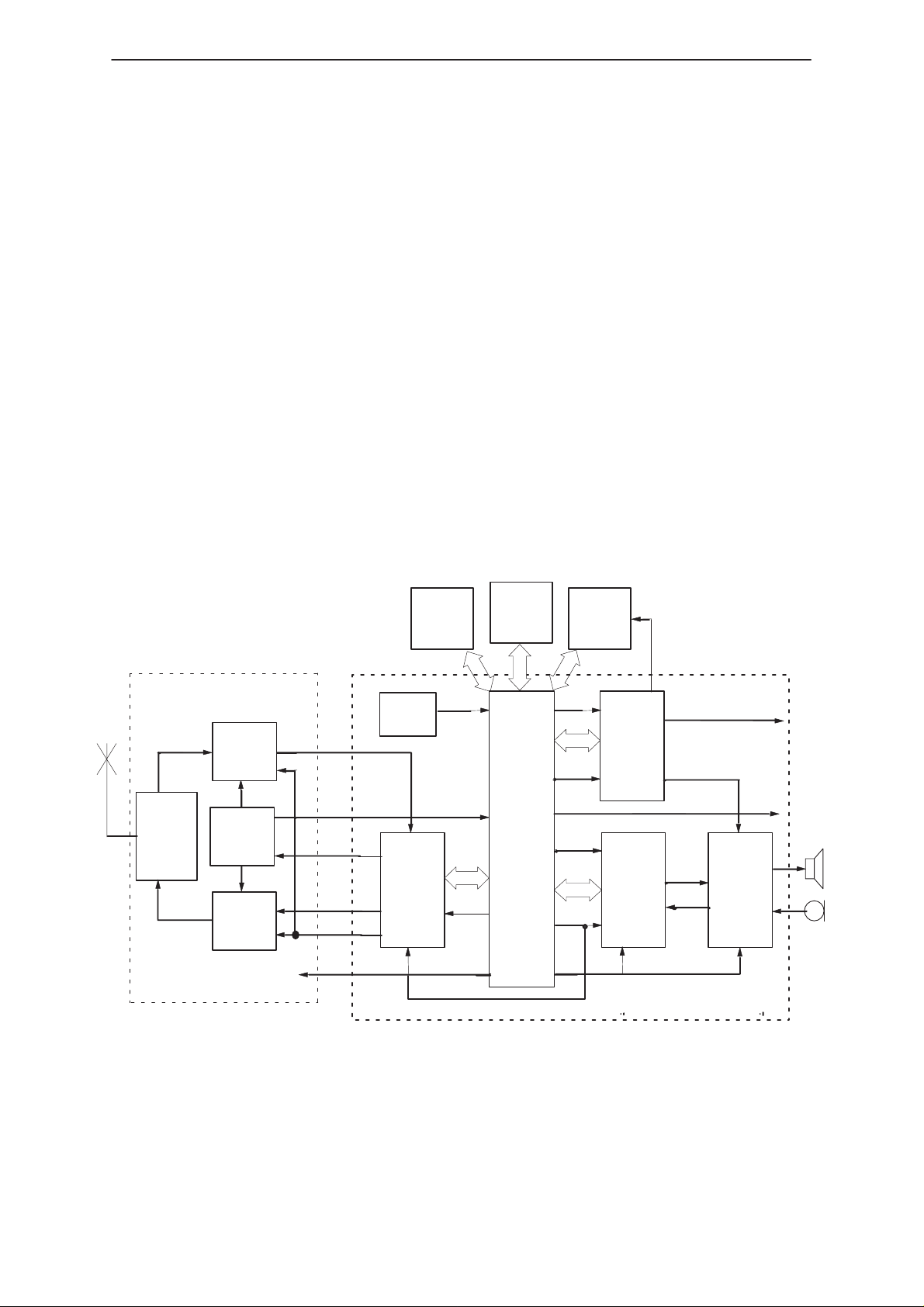
The transceiver electronics consists of the Radio Module (RF + BB blocks),
the UI–module and the display module. The UI–module is connected to the
Radio Module with a connector and display module is connected to
UI–module by solder joint. BB blocks and RF blocks are interconnected with
PCB wiring. The Transceiver is connected to accessories via a bottom
system connector with charging and accessory control.
The BB blocks provide the MCU and DSP environments, Logic control IC,
memories, audio processing and RF control hardware (RFI2). On board
power supply circuitry delivers operating voltages for BB blocks. RF blocks
have regulators of their own.
The general purpose microcontroller, Hitachi H8/3001, communicates with
the DSP, memories and Logic control IC with an 8–bit data bus.
The RF block is designed for a handportable phone which operates in the
GSM system. The purpose of the RF block is to receive and demodulate the
radio frequency signal from the base station and to transmit a modulated RF
signal to the base station.
PAMS
Technical Documentation
DUPLEX
FILTER
RF BLOCK
RX
RX
SYNTE
SYNTE
TX
TX
Keyboard
SYSTEM
ASIC
Clk
13 M
IF 13 M
Clk 13 M
AFC
TXI,TXQ
TXC
RF CONTROL
SIM
PSCLD
RESET
RFI2
Figure 1. Block Diagram – BB/RF Modules
Display
RESET
Clk
13 M
Clk
13 M
RESET
MCU
DSP
Clk 512 k,
RESET
M2BUS
FBUS
AUDIO
Clk 8 k
SYSTEM BLOCK
Page 3 – 6
issue 3 12/98
Page 7

PAMS
NHE–8/9
Technical Documentation
Power Distribution
The power supply is based on the ASIC circuit PSCLD. The chip consists of
regulators and control circuits providing functions like power up, reset and
watchdog functions. External buffering is required to provide more current.
The MCU and the PSCLD circuits control charging together, detection being
carried out by the PSCLD and higher level intelligent control by the MCU.
Charger voltages as well as temperature and size of the battery are
measured by internal ADC of MCU or RFI (depending on the state of the
phone). MCU measures battery voltage via DSP by means of RFI2 internal
ADC.
Baseband Module
The GJ3 module is used in GSM products. The baseband is implemented
using DCT2 core technology. The baseband is built around one DSP,
System ASIC and the MCU. The DSP performs all speech and GSM
related signal processing tasks. The baseband power supply is 3V except
for the A/D and D/A converters that are the interface to the RF section.
The A/D converters used for battery and accessory detection are
integrated into the same device as the signal processing converters.
System Module
The audio codec is a separate device which is connected to both the DSP
and the MCU. The audio codec support the internal and external
microphone/earpiece functions. External audio is connected in a dual
ended fashion to improve audio quality together with accessories.
The baseband implementation support a 32.768 kHz sleep clock function
for power saving. The 32.768 kHz clock is used for timing purposes during
inactive periods between paging blocks. This arrangement allows the
reference clock, derived from RF to be switched off.
The baseband clock reference is derived from the RF section and the
reference frequency is 13 MHz. A low level clipped sinusoidal wave form
is fed to the ASIC which acts as the clock distribution circuit. The DSP is
running at 39 MHz using an internal PLL. The clock frequency supplied to
the DSP is 13 MHz. The MCU bus frequency is the same as the input
frequency. The system ASIC provides both 13 MHz and 6.5 MHz as
alternative frequencies. The MCU clock frequency is programmable by the
MCU. The nhe–8/9 baseband uses 13 MHz as the MCU operating
frequency. The RF A/D, D/A converters are operated using the 13 MHz
clock supplied from the system ASIC
The power supply and charging section supplies Lithium Ion and NiMH
type of battery technology. The battery charging unit is designed to accept
constant current type of chargers, that are approved by NMP.
The power supply IC, contains four different regulators. The output voltage
from two of the regulators are 3.15V nominal. A third regulator controls an
external boost transistor for a 3.15V ’high’ current supply. The last
regulator supplies the SIM card voltage, which is 4.9V.
issue 3 12/98
Page 3 – 7
Page 8
NHE–8/9
g
System Module
Technical Documentation
Technical Specifications
The Baseband in nhe–8/9 Operates in the following Modes
Active, as during a call or when baseband circuitry is operating
Sleep, in this mode the clock to the baseband is stopped and
timing is kept by the 32.768 kHz oscillator. All Baseband
circuits are powered
Acting dead, in this mode the battery is charged but only
necessary functions for charging are running
Power off, in this mode all baseband circuits are powered off.
The regulator IC N300 is powered
External Signals and Connections
Table 1. List of Connectors
Connector Name Code Notes Specifications / Ratings
PAMS
System Connector 5469007 X100
SIM Connector 5409033 X102
Table 2. System Connector X100
Pin Name Parameter Min Typ Max Unit Remark
1, 7,
18,
20
2 V_OUT Accessory Out-
3 XMIC
GND Charger & Sys-
tem Ground
put Supply
External Micro-
ID
phone Input
Endless No Accessory
IR Link 2.22 2.39 2.56 V Infra Red Link connected
Headset 1.7 1.9 2.05 V Headset Adapter Con-
Compact HF 1.15 1.3 1.4 V Compact HF Connected
0
800
3.40 9.3 V Output Current 50 mA.
8 50 mV The maximum value corre-
0
1500VmA
Measuring Reference
Max Value for Charger
Peaks
sponds to 0 dBm network
level with input amplifier
gain set to 20 dB. Typical
value is maximum value
–16 dB.
nected
4 EXT_RF External RF con-
trol input
5 TX FBUS transmit
6 MBUS Serial
Control
Bus
Page 3 – 8
”0”
”1”
0 0.5 V External RF in use
2.4 3.2 V Internal antenna in use
0 0.5
2.4 3.2
0
2.4
0.5
3.2
Accessory FBUS transmit
signal, Serial data bus. The
signal has a pull–up inside
the ASIC.
Baud rate 9.6 – 115.2kBit /
s.
V
General Purpose Control
V
and Test Control Bus
issue 3 12/98
Page 9
PAMS
NHE–8/9
Technical Documentation
Table 2. System Connector X100 (continued)
8 SGND Signal ground 0 0 V Measuring Reference for
Audio signals. 47 ohm to
9 XEAR
10 HOOK Acces-
11 RX FBUS receive
External Speaker 0 32 500 mV Connected to Audio Codec
Inverted Output. Typical
level corresponds to –16
dBmO network level with
volume control in nominal
position 8db below maxi-
mum. Maximum 0 dBm0
max. volume codec gain
MUTE ON
OFF
OFF
sory
Hook
Signal
ON 2.4
0
1 1.5
0 0.5 V
2.4 3.2 V
0.5
1.7
0.5
3.2
V
V
V
V
Baseband has 4.7 kohm
Accessory FBUS receive
signal, Serial data bus.
Baud rate 9.6 – 115.2kBit /
Phone has a pull–up resis-
System Module
RemarkUnitMaxTypMinParameterNamePin
Audio Ground
–6dB.
HF Speaker Mute
HF Speaker Active
HOOK OFF
HOOK ON
Pull–up
s.
tor.
13 BGND GND 0 0 0 V Battery GND
14 BTEMP Battery Temper-
ature
15 BSI Battery Size 0 0 3.3 V Used for SIM Card Detec-
16 VBatt Battery Voltage 5.3 6 9.3 V Main Power Supply
12,
17,
19
V_IN Charger supply
Voltage
0 0 3.3 V Also used for Vibration
Alert
tion
9.8
12
10.3
14
10.8
16
VVFast Charger ACH–6 (780
mA)
Standard Charger ACH–8
(265mA)
issue 3 12/98
Page 3 – 9
Page 10

NHE–8/9
System Module
PAMS
Technical Documentation
Table 3. SIM Connector X102
Pin Name Parameter Logic
Level
1 GND, C5 GND 0 0 V Digital GND
2,6 VSIM, C1,C6SIM Supply
Voltage
3 SDATA,
C7
4 SRES, C2 SIM Reset ”1”
5 CLK, C3 SIM Clock ”1”
SIM DA TA
VI
VO
”1”
”0”
”1”
”0”
”0”
”0”
Min Typ Max Unit Remark
4.8 4.9 5.0 V Tr, max.
2V/us max
200 us. T
max. 200 us.
0.7xVSIM
0
0.7xVSIM
0
VSIM–0.7
0
0.7xVSIM
0
VSIM
0.8
VSIM
0.4
VSIM
0.6
VSIM
0.5
V
V
V Clock fre-
quency mini-
mum 1 MHz if
clock stopping
not allowed
Note1.
f
Note 1. VSIM supply voltage may be selected to 3 V to meet 3V SIM card specifications. ( Voltage
range 3.1 to 3.3 V). The values in NO TAG will be different, values only valid for ”5 volt SIM card”.
Page 3 – 10
issue 3 12/98
Page 11
PAMS
S
PSCLD
NHE–8/9
Technical Documentation
Table 4. User Interface Connector X101
4
5 VL Display Sup-
6 SYSRE-
7 GND Ground 0 V
8 KEYLIGHT Keboard
9 LCDLIGHT Display
10 BUZZER PWM signal-
11 GND Ground 0 V
GND Ground 0 V
3.0 3.2 V
ply
Reset
ETX
Light
Light
Buzzer con-
trol
”1” 2.4 3.2 V
”0” 0 0.6 V
”1”
”0”
”1”
”0”
2.8
0
2.8
0
0 3.2 V
3.2
0.2
3.3
0.2
System Module
Edge sensi-
tive
V Max 1 mA
can be
drawn from
N300
(PSCLD)
V Max 1 mA
can be
drawn from
N300
(PSCLD)
12 GENSCLK Serial clock
13 GENSD Serial data
14 LCDENX LCD enable
15 VBatt Battery Sup-
ply
18 XPWRON Power ON/
OFF
”1” 2.4 3.2 V
”0” 0 0.6 V
”1” 2.4 3.2 V
”0” 0 0.6 V
”1” 2.4 3.2 V
”0” 0 0.6 V
5.3 9.3 V
”1” 5.3 9.3 V
”0” 0 0.4 V
1.083 MHz
Pulled up to
Vbatt inside
.
issue 3 12/98
Page 3 – 11
Page 12
NHE–8/9
System Module
Table 4. User Interface Connector X101 (continued)
19 EARN Earphone 0 14 220 mV Connected
Technical Documentation
to Audio Co-
dec Inverted
Output. Typical level cor-
responds to
–16 dBmO
network level
with volume
control giv-
ing nominal
RLR
(=+2dB) 8
db below
max. Max
level is
0dBmO with
max volume
(codec gain
–11 db)
PAMS
20 EARP Earphone 0 14 220 mV Connected
to Audio Co-
dec non Inverted Out-
put. Typical
level corre-
sponds to
–16 dBmO
network level
with volume
control giv-
ing nominal
RLR
(=+2dB) 8
db below
max. Max
level is
0dBmO with
max volume
(codec gain
–11 db)
21 ROW(0) ROW(0) In-
put
22 ROW(1) ROW(1) In-
put
”1”
”0”
”1”
”0”
2.4
0
2.4
0
3.2
0.6
3.2
0.6
V
V
23 ROW(2) ROW(2) In-
24 ROW(3) ROW(3) In-
25 ROW(4) ROW(4) In-
Page 3 – 12
put
put
put
”1”
”0”
”1”
”0”
”1”
”0”
2.4
0
2.4
0
2.4
0
3.2
0.6
3.2
0.6
3.2
0.6
V
V
V
issue 3 12/98
Page 13
PAMS
NHE–8/9
Technical Documentation
Table 4. User Interface Connector X101 (continued)
26 ROW(5) ROW(5) In-
put
27 COL(0) COL(0) Out-
put
28 COL(1) COL(1) Out-
put
29 COL(2) COL(2) Out-
put
30 COL(3) COL(3) Out-
put
31 GND Ground 0 V
”1”
”0”
”1”
”0”
”1”
”0”
”1”
”0”
”1”
”0”
2.4
0
2.6
0
2.6
0
2.6
0
2.6
0
3.2
0.6
3.2
0.4
3.2
0.4
3.2
0.4
3.2
0.4
System Module
V Also used for
data control
for LCD
V
V
V
V
Table 5. DAI interface connecting test pads
Pin Name Parameter Logic
Level
1 CODECB(0) Audio codec
clock
2 CODECB(4) DSP Serial
Data Receive
3 CODECB(5) DSP Serial
Data Trans-
mit
4 CODECB(1) Audio codec
sync
5 VL Digital Supply 3.0 3.3 V test pin J320
6 GND GND 0 0.2 V test pin J321
”1”
”0”
”1”
”0”
”1”
”0”
”1”
”0”
Min Typ Max Unit Remark
2.4
0
2.4
0
2.4
0
2.4
0
3.2
0.6
3.2
0.6
3.2
0.6
3.2
0.6
V Audio Codec clock
for DAI measure-
ments; test pin
J316
V Serial PCM data
receive for DAI
measurements;
test pin J317
V Serial PCM data
transmit for DAI
measurements;
test pin J318
V Audio Codec frame
synchronisation for
DAi measure-
ments; test pin
J319
issue 3 12/98
Page 3 – 13
Page 14
NHE–8/9
System Module
Technical Documentation
Internal Signals and Connections
Table 6. SYS_CONN Block Connections
Name of Signal or Bus Type Notes References
XEAR/MUTE IN External earphone input from AU-
DIO block to System connector
SGND OUT Used as reference for external audio
XMIC/ID OUT External Microphone output from
System connector to AUDIO block
EXT_RF OUT External RF control output from
System Connector to CCPU block
BTYPE OUT Battery type
BTEMP OUT Battery temperature
HOOK OUT Accessory Interrupt
CHARGER+ OUT Charger positive contact
GND Ground
PAMS
VBATT IN Battery Supply Input to Power Block
MBUS I/O Serial Data Bus to MCU
V_OUT OUT External Accessory supply voltage
TX OUT Accessory FBUS digital data output
RX IN Accessory FBUS digital data input
RF I/O External RF connector signal
Page 3 – 14
issue 3 12/98
Page 15
PAMS
NHE–8/9
Technical Documentation
Table 7. Audio Block Connections
Name of Signal or Bus Type Notes References
SGND OUT Negative Output From N200 (Co-
dec) Pin 2 used as reference for ex-
ternal audio
CODECB(5:0) IN/OUT Serial Digital Bus for Speech trans-
mission to/from CCPU Block
SCONB(5:0) IN/OUT Serial Control Bus from CCPU Block
XMIC IN External Microphone Input from
System Connector
MICP IN Positive Microphone input from in-
ternal Microphone
MICN IN Negative Microphone input from in-
ternal Microphone
XEAR OUT Positive Output from N200 (CO-
DEC)
EARN OUT Negative Earpiece output signal
from N200 (Codec)
EARP OUT Positive Earpiece output signal from
N200 (Codec)
BUZZER OUT Buzzer Output to User Interface
Connector
ACCDET OUT LP Filtered Signal from XMIC input
for Accessory Detection. Connected
to CCPU and RFI Block
System Module
Table 8. Keyboard Block Connections
Name of Signal or Bus Type Notes References
KEYB(9:0) IN/OUT Keyboard input/output
PWRONX OUT Power on signal to Power Block
COL(3:0) OUT Column Output to Keyboard con-
nector X101
ROW(5:0) IN Row inputs from keyboard Connec-
tor X101
PWRX IN Power On Signal input from Key-
board Connector
Active Low
issue 3 12/98
Page 3 – 15
Page 16
NHE–8/9
System Module
Table 9. Power Block Connections
Name of Signal or Bus Type Notes References
MBUS(2:0) I/O Serial Data Bus to MCU
CODECB(5:0) IN/OUT Serial Synchronous Data Bus for
DAI and Testing
MCUP4(7:0) I/O MCU Port 4 Bus
SCONB(5:0) I/O Serial Control Bus for Regulator IC
Control
SIMI(5:0) I/O SIM Card Signals from CCPU Block
BSI IN Battery Size Signal from System
Connector
BTEMP IN Battery Temperature Signal from
System Connector
CHARGER IN Charger Supply Input to Power
Block
GND Ground
Technical Documentation
PAMS
PWRONX IN Power On Signal from Keyboard
Block
SLEEPIX IN Sleep Control Signal from CCPU MCUMEMC(6)
VBAT IN Battery Supply Input to Power Block
VBATT OUT Battery Voltage to UI module
VBATT OUT Battery Power Supply to RF VBAT
CHARGE I/O Charge Detection Signal to CCPU
V_OUT OUT Accessory Power Supply
VLCD OUT Supply Voltage to LCD and Driver
VA OUT Supply voltage to Audio / analog cir-
cuitry.
VSL OUT Supply voltage and sleep mode sup-
ply
VL OUT Supply voltage for logic circuitry
SLEEPOX OUT Sleep signal to control RF VCXO Active Low, VXOENA
PURX OUT Power Up Reset to CCPU Block Active Low
M2BUS I/O Serial Control Bus to System Con-
nector
SIMCARD(3:0) I/O SIM Card SIgnals to Card Connec-
tor X102
LIGHTC(1:0) OUT Display & Keyboard Light Control
signals
ADCONV(5:0) OUT BSI, BTEMP, VBAT and VCAR V olt-
age to Baseband A/D Converter
Page 3 – 16
issue 3 12/98
Page 17
PAMS
NHE–8/9
Technical Documentation
Table 10. CCPU Block Connections
Name of Signal or Bus Type Notes References
DSP_DATA(15:0) I/O 16 Bit DSP Data Bus
DATA(7:0) I/O 8 Bit MCU Data Bus
RFI_DATA(11:0) I/O 12 Bit RFI2 Data Bus
MBUS(2:0) I/O Serial Data Bus to MCU
CODECB(5:0) I/O DSP and Audio Codec Serial Bus
ACCES(1:0) I/O Accessory FBUS data
CPUAD(5:0) IN Input to MCU A/D Converter
PURX IN Power Up Reset
RFCLK IN System Clock from RF
RFDAX IN Data Available Signal From RFI2
CHARGE I/O Charger Presence Signal
HEADS IN Accessory Interrupt
RFCGND IN Reference Ground for RFCLK
System Module
RFICLK OUT 13 MHz Clock to RFI2
DSPINT(3:0) IN DSP Interrupt signals
DSPGENP(3:0) OUT DSP General Purpose Outputs
SCONB(5:0) OUT/IN Control Bus for Power Supply IC,
Display Driver and Audio Codec
DSP_ADDR(15:0) OUT DSP Address Bus
MEMC(6:0) OUT Chip Select and Memory control sig-
nals from MCU
MCUP4(7:0) I/O MCU Port 4 Signals
SIM(5:0) I/O SIM Card SIgnals to Power Block
DMEMC(3:0) OUT DSP Memory Control Signal Bus
RFO CONT OUT External RF output control
ADDR(23:0) OUT MCU Address Bus
RFCONT(7:0) OUT RF and Synthesizer Control Signal
Bus
RFIADC(5:0) OUT RFI2 Address and Control signal
Bus
KEYB(9:0) OUT/IN Keyboard ROW and Column Sig-
nals
issue 3 12/98
Page 3 – 17
Page 18
NHE–8/9
System Module
Table 11. DSP_MEM Block Connections
Name of Signal or Bus Type Notes References
DSPMEMC(3:0) IN DSP Memory Control Signals from
CCPU Block
DSP_ADDR(15:0) IN 16–Bit DSP Address Bus from
CCPU Block
DSP_DATA(15:0) I/O 16–Bit DSP Data Bus from CCPU
Block
Table 12. MCU_MEM Block Connections
Name of Signal or Bus Type Notes References
MEMC(6:0) IN Memory Control Signals from CCPU
Block
ADR(23:0) IN 23–Bit MCU Address Bus from
CCPU Block
DA TA(7:0) I/O 8–Bit MCU Data Bus from CCPU
Block
Technical Documentation
PAMS
Table 13. RFI Block Connections
Name of Signal or Bus Type Notes References
RFIDATA(11:0) I/O 12 Bit Data Bus Between RFI2 and
CCPU Block
DSPINT(3:0) OUT Interrupt to CCPU Block
AUXAD(5:0) IN Baseband Measurement A/D Con-
verter Signals to RFI2 Block
RFIADC(5:0) OUT 4 Bit Address and 2 Bit Control Bus
from CCPU Block
VXOENA IN Sleep signal to control RFI2 analog
power supply
VBATT IN Battery Supply Voltage from Power
Block
RFICLK IN 13 MHz clock from CCPU Block
RFIDAX OUT Data Available Signal From RFI2
RXQ IN Input Signal From RF
RXI IN Input signal from RF
VREF 2.5V OUT Reference Voltage to RF
AFC OUT AFC Voltage to RF VCXO
Active Low, SLEEPOX
TXC OUT Power Ramp Control Signal to RF
TXIN OUT Negative In Phase Signal to RF
TXIP OUT Positive In Phase Signal to RF
TXQN OUT Negative Quadrature Signal to RF
TXQP OUT Positive Quadrature Signal to RF
RFIPORT(6:0) OUT Parallel Port From RFI Block
Page 3 – 18
issue 3 12/98
Page 19
PAMS
C
reg-
tor
WRCreg-
tor
C
reg-
tor
C
C
C
NHE–8/9
Technical Documentation
Table 14. AC and DC Characteristics of the RF–baseband signals
Signal
name
VBATT bat-
VXOENA ASICRF
RXPWR ASI
FromTo Parameter Min Typical Max Unit Function
Voltage 5.3 6.0 9.3 V
RF
tery
Current 1500mA
Logic high ”1” 2.4 3.15 3.3 V Synth. regulator ON
regula-
Logic low ”0” 0 0.5 V Synth. regulator OFF,
tor
Current 0.5 mA
timing inaccuracy 10 us
Logic high ”1” 2.4 3.15 3.3 V RX supply voltage ON
RF
Logic low ”0” 0 0.5 V RX supply voltage OFF
ula-
Current 0.5 mA
System Module
Supply voltage for RF
vcxo voltage ON,
VCXO voltage OFF
SYNTHP
TXPWR ASI
SENA1 ASI
SDATA ASI
ASI
Logic high ”1” 2.4 3.15 3.3 V RF regulators ON
RF
Logic low ”0” 0 0.5 V RF regulators OFF
ula-
Current 1.0 mA
Logic high ”1” 2.4 3.15 3.3 V TX supply voltage ON
RF
Logic low ”0” 0 0.5 V TX supply voltage OFF
ula-
Current 0.5 mA
Logic high ”1 2.4 3.15 3.3 V
PLL
Logic low ”0” 0 0.8 V
Current 50 uA
Load capacitance 10 pF
Logic high ”1 2.4 3.15 3.3 V
PLL
Logic low ”0” 0 0.8 V
Load resistance 10 koh
Load capacitance 10 pF
Data rate frequency 3.25 MH
Dual PLL Enable
Synthesizer data
m
z
SCLK ASI
issue 3 12/98
Logic high ”1 2.4 3.15 3.3 V
PLL
Logic low ”0” 0 0.8 V
Load impedance 10 koh
Load capacitance 10 pF
Data rate frequency 3.25 MH
Synthesizer clock
m
z
Page 3 – 19
Page 20
NHE–8/9
C
System Module
Table 14. AC and DC Characteristics of the RF–baseband signals (continued)
PAMS
Technical Documentation
Signal
name
TXP ASI
RFC VCTCXASI
PDATA0 RFI2LNA
m
RF
C
O
LNA
RFI
2
FunctionUnitMaxTypicalMinParameterToFro
Logic high ”1” 2.4 3.15 3.3 V
Logic low ”0” 0 0.8 V
Load Resistance 50 koh
Load Capacitance 10 pF
Timing inaccuracy 1 us
Frequency 13 MH
Signal amplitude 0.4 1.0 3.0 Vpp
Load Resistance 10 koh
Load Capacitance 5 pF
Logic high ”1” 2.4 3.15 3.3 V Nominal front end gain
Logic low ”0” 0 0.8 V Reduced front end gain
Current 0.1 mA Nominal front end gain
Transmitter power control enable
m
High stability clock sig–
z
nal for the locig circuits
m
PDATA1 RFI
2
PDATA2 RFI
2
PDATA3 RFI
2
PDATA4 RFI
2
PDATA5 RFI
2
Logic high ”1” 2.4 3.15 3.3 V
Logic low ”0” 0 0.5 V
Current 10 uA
Logic high ”1” 2.4 3.15 3.3 V
Logic low ”0” 0 0.5 V
Current 10 uA
Logic high ”1” 2.4 3.15 3.3 V
Logic low ”0” 0 0.5 V
Current 10 uA
Logic high ”1” 2.4 3.15 3.3 V
Logic low ”0” 0 0.5 V
Current 10 uA
Logic high ”1” 2.4 3.15 3.3 V
Logic low ”0” 0 0.5 V
Current 10 uA
Not used !
Not used !
Not used !
Not used !
Not used !
Page 3 – 20
issue 3 12/98
Page 21
PAMS
C
O
O
O
VCTCXO
RXIN
FRFT2
signal to baseband
NHE–8/9
Technical Documentation
Table 14. AC and DC Characteristics of the RF–baseband signals (continued)
Signal
name
AFC RFI
RXIP /
m
2
CR
Voltage 0.26 3.94 V
VCT
X
Resolution 11 bits
Load impedance
(dynamic)
Noise Voltage 500
Settling time 1 ms
RFI
Output level 25 570 mVppDifferential RX 13 MHz
Source impedance 300 ohm
Load Resistance 10 koh
Load Capacitance 5 pF
10 koh
m
uVrm
s
m
System Module
FunctionUnitMaxTypicalMinParameterToFro
Automatic frequency
control signal for
VCTCX
10...10000 Hz
TXIP/
TXIN
RFI2CR
FRT
Phase Imbalance 2 deg
Amplitude Imbal-
ance
Differential voltage
swing
Differential Offset
voltage
Diff. Offset voltage
temp. dependence
DC level 2.0162.1 2.40 V
Offset voltage +–10mV
Source Impedance 50 ohm
Load Resistance 16 koh
Load Capacitance 10 pF
Resolution 8 bits
DNL +–0.9LSB
2.23 2.40 2.57 Vpp
1 dB
+–4.
mV
7
+–
2
m
Differential in–phase
TX baseband signal for
the RF modulator
TXQP/
TXQN
issue 3 12/98
RFI2CR
FRT
INL + –1 LSB
Group delay mis-
match
Same spec as for TXIP / TXIN Differential quadrature
100 ns
phase TX baseband
signal for the RF modulator
Page 3 – 21
Page 22
NHE–8/9
tro
trol
System Module
Table 14. AC and DC Characteristics of the RF–baseband signals (continued)
PAMS
Technical Documentation
Signal
name
TXC RFI
VREF 2.5 RFI2RF Voltage level 2.493 V RF reference voltage
m
CR
2 FRT
Voltage Max 3.86 3.94 V
Voltage Min 0.26 0.34 V
Vout temperature
dependence
Source Impedance 50 ohm
Input resistance 10 koh
Input capacitance 10 pF
Settling Time 10 us
Noise level 500
Resolution 10 bits
DNL +–0.9LSB
INL + –4LSB
10 LSB
m
uVrm
s
Transmitter power control, CRFRT gain con-
0...200kHz
FunctionUnitMaxTypicalMinParameterToFro
l
RFO_CO
NT U
RFOUT RF OU
RFCGND ASICRF RFC signal ground
MC
Logic high ”1” 2.4 3.3 V
RF
Logic low ”0” 0 0.6 V
T
External RF control
2 W External RF signal
from/to bottom connector
Page 3 – 22
issue 3 12/98
Page 23

PAMS
NHE–8/9
Technical Documentation
Functional Description
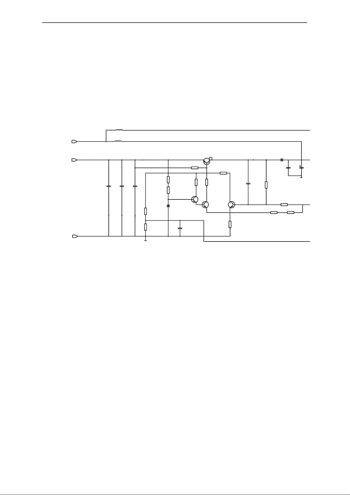
Power Supply
Vxoena
VBAT
V305
CHARGER +
L107
L108
CHGND
BGND
R344
C340
CHARGER
UNIT
V100
L101
GND
GND
AGND
L311
N451
4.50 V
L312
PSCLD
N300
VA
3.16 V
VSIM
5/3V
VRFI
N450
Z152
Z151
V306
GND
VSL
VSLRC
3.16 V
D151; pin 124
VSLC
3.16 V
D151
D401
D403
System Module
VBATT to RF
VBATT to UI module
VL
3.16 V
L306
Z150
Z153
Z451 VLRFI
VLCD
3.16 V3.16 V
VLMCU
VLDSP
D152
D404
D405
3.16 V
D150
D400
3.16 V
N450
Figure 2. Power Distribution Diagram.
The power supply for the baseband is the main battery. A charger input is
used to charge the battery. Two different chargers can be used for
charging the battery. A switch mode type fast charger that can deliver 780
mA and a standard charger that can deliver 265 mA. Both chargers are of
constant current type.
The baseband has one power supply IC, N300 delivering power to the
different parts in the baseband. There are two logic power supply and one
analog power supply. The analog power supply VA is used for analog
circuits such as audio codec, N200 and microphone bias circuitry. Due to
the current consumption and the baseband architecture the digital supply
is divided into two parts.
Both digital power supply rails from the N300, PSCLD are used to
distribute the power dissipation inside N300, PSCLD. The main logic
power supply VL has an external power transistor, V306 to handle the
power dissipation that will occur when the battery is fully charged or during
charging.
issue 3 12/98
Page 3 – 23
Page 24
NHE–8/9
W
A
System Module
D151, ASIC and the MCU SRAM, D403 are connected to the same logic
supply voltage. All other digital circuits are connected to the main digital
supply.
Charging Control Switch Functional Description
The charging switch circuit diagram is shown below. The figure is for
reference only.
L303
L300
VBAT
PAMS
Technical Documentation
VB
V304 V305
C303
R343
V302
R308
V303
R327
R342
V311
R304
C304
R308
R309
CHARGER
GND
C300 C301 C302
R302
R303
R301
R326
V301
Figure 3. Charge Switch Circuit Diagram
The charging switch transistor V304 controls the charging current from the
charger input to the battery. During charging the transistor is forced in
saturation and the voltage drop over the transistor is 0.2–0.4V depending
upon the current delivered by the charger. Transistor V304 is controlled by
the PWM output from N300, via resistors R309, R308 and transistor V311.
The output from N300 is of open drain type. When transistor V304 is
conducting the output from N300 pin is low. In this case resistors R305
and R306 are connected in parallel with R304. This arrangement
increases the base current thru V304 to put it into saturation.
C308
C305
P
R306R305
Transistors V304, V302, V303 and V311 forms a simple voltage regulator
circuitry. The reference voltage for this circuitry is taken from zener diode
V301. The feedback for the regulator is taken from the collector of V304.
When the PWM output from N300 is active, low, the feedback voltage is
determined by resistors R308 and R309. This arrangement makes the
charger control switch circuitry to act as a programmable voltage regulator
with two output voltages depending upon the state of the PWM output
from N300. When the PWM is inactive, in high impedance state, the
feedback voltage is almost the same as on the collector of V304. Due to
the connection the voltage on V303 and V311 emitters are the same.
The feedback means that the system regulates the output voltage from
V304 in such a way that the base of V303 and V311 are at the same
voltage. The voltage on V302 is determined by the V301 zener voltage.
Page 3 – 24
issue 3 12/98
Page 25

PAMS
NHE–8/9
Technical Documentation
The darlington connection of V303 and V302 service two purposes ; 1 the
load on the voltage reference V301 is decreased, 2 the output voltage on
V304 is decreased by the VBE voltage on V302 which is a wanted feature.
The voltage reduction allows a relative temperature stable zener diode to
be used and the output voltage from V304 is at a suitable level when the
PWM output from N300 is not active.
The circuitry is self starting which means that an empty battery is initially
charged by the regulator circuitry around the charging switch transistor.
The battery is charged to a voltage of maximum 4.8V. This charging
switch circuitry allows for both NiCd, NiMH and Lithium type of batteries to
be used. At the same time it will secure that the battery will not over
charge in case one cell is short circuited.
When the PWM output from N300 is active the feedback voltage is
changed due to the presence of R308 and R309. When the PWM is active
the charging switch regulator voltage is set to 9.3V maximum. This means
that even if the voltage on the charger input exceeds 11.5V the battery
voltage will not exceed 9.3 V. This protects N300 from over voltage even if
the battery was to be detached while charging.
System Module
The RC network C304, R308 and R309 also acts as a delay circuitry when
switching from one output voltage to an other. This happens when the
PWM output from N300 is pulsing. The reason for the delay is to reduce
the surge current that will occur when V304 is put into conducting state.
Before V304 is put in conducting state there is a significant voltage drop
over V304. The energy is stored in capacitors in the charger and these
capacitors must first be drained in order to put the charger in constant
current mode. This is done by discharging the capacitors into the battery.
The delay caused by C304 will reduce the surge current thru V304 to an
acceptable value.
R301 and R326 are used to regulate the zener current. During charging
with empty battery the zener voltage might drop due to low zener current
but this is no problem since the regulator is operating in constant current
mode while charging. The zener voltage is more important when the
charger voltage is high or in case that the PWM output from N300 is
inactive. In this case the charger idle voltage is present at the charger
supply pins.
R300 and R327 together with V304 forms a constant current source. The
surge current limitation behavior is frequency dependent since L107 is an
inductor. The purpose of this circuitry is to reduce the surge current thru
V304 when it is put in conducting state. Due to the low resistance value
required in L107 this arrangement is not very effective and the RC
network R308, R309 and C304 contributes more to the surge current
reduction.
V305 is a schottky diode that prevents the battery voltage from reverse
biasing V304 when the charger is not connected. The leakage current for
V305 is increasing with increasing temperature and the leakage current is
passed to ground via R308, V311 and R304.
issue 3 12/98
Page 3 – 25
Page 26

NHE–8/9
System Module
This arrangement prevents V304 from being reversed biased as the
leakage current increases at high temperatures.
Components L107, C300, C301, C302 and L108 forms a filter for EMC
attenuation. The circuitry reduces the conductive EMC part from entering
the charger cable causing an increase in emission as the cable will act as
an antenna.
V100 is a 18V transient suppressor. V100 protects the charger input and
in particular V304 for over voltage. The cut off voltage is 18V with a
maximum surge voltage up to 25V. V100 also protects the input for wrong
polarity since the transient suppressor is bipolar.
Power Supply Regulator PSCLD, N300
The power supply regulators are integrated into the same circuit N300.
The power supply IC contains three different regulators. The main digital
power supply regulator is implemented using an external power transistor
V306. The other two regulators are completely integrated into N300.
PAMS
Technical Documentation
PSCLD, N300 External Components
N300 performs the required power on timing. The PSCLD, N300 internal
power on and reset timing is defined by the external capacitor C330. This
capacitor determines the internal reset delay, which is applied when the
PSCLD, N300 is initially powered by applying the battery. The baseband
power on delay is determined by C311. With a value of 10 nF the power
on delay after a power on request has been active is in the range of
50–150 ms. C310 determines the PSCLD, N300 internal oscillator
frequency and the minimum power off time when power is switched off.
The sleep control signal from the ASIC, D151 is connected via PSCLD,
N300. During normal operation the baseband sleep function is controlled
by the ASIC, D151 but since the ASIC is not powered up during the
startup phase the sleep signal is controlled by PSCLD, N300 as long as
the PURX signal is active, low. This arrangement ensures that the 13 MHz
clock provided from RF to the ASIC, D151 is started and stable before the
PURX signal is released and the baseband exits reset. When PURX is
inactive, high, sleep control signal is controlled by the ASIC D151.
To improve the performance of the analog voltage regulator VA an
external capacitor C329 has been added to improve the PSRR.
N300 requires capacitors on the input power supply as well as on the
output from each regulator to keep each regulator stable during different
load and temperature conditions. C305 and C308 are the input filtering
capacitors. Due to EMC precautions a filter using C305, L300 and C308
has been inserted into the supply rail. This filter reduces the high
frequency components present at the battery supply from exiting the
baseband into the battery pack. The regulator outputs also have filter
capacitors for power supply filtering and regulator stability. A set of
different capacitors are used to achieve a high bandwith in the
suppression filter.
Page 3 – 26
issue 3 12/98
Page 27

PAMS
NHE–8/9
Technical Documentation
PSCLD, N300 Control Bus
The PSCLD, N300 is connected to the baseband common serial control
bus, SCONB(5:0). This bus is a serial control bus from the ASIC, D151 to
several devices on the baseband. This bus is used by the MCU to control
the operation of N300 and other devices connected to the bus. N300 has
two internal 8 bit registers and the PWM register used for charging control.
The registers contains information for controlling reset levels, charging
HW limits, watchdog timer length and watchdog acknowledge.
The control bus is a three wire bus with chip select for each device on the
bus and serial clock and data. From PSCLD, N300 point of view the bus is
used as write only to PSCLD. It is not possible to read data from PSCLD,
N300 by using this bus.
The MCU can program the HW reset levels when the baseband
exits/enters reset. The programmed values remains until PSCLD is
powered off, the battery is removed. At initial PSCLD, N300 power on the
default reset level is used. The default value is 5.1 V with the default
hysteresis of 400 mV. This means that reset is exit at 5.5 V when the
PSCLD, N300 is powered for the first time.
System Module
The watchdog timer length can be programmed by the MCU using the
serial control bus. The default watchdog time is 32 s with a 50 %
tolerance. The complete baseband is powered off if the watchdog is not
acknowledged within the specified time. The watchdog is running while
PSCLD, N300 is powering up the system but PURX is active. This
arrangement ensures that if for any reason the battery voltage doesn’t
increase above the reset level within the watchdog time the system is
powered off by the watchdog. This prevents a faulty battery from being
charged continuously even if the voltage never exceeds the reset limit. As
the time PURX is active is not exactly known, depends upon startup
condition, the watchdog is internally acknowledged in PSCLD when PURX
is released. This gives the MCU always the same time to respond to the
first watchdog acknowledge.
Baseband power off is initiated by the MCU and power off is performed by
writing the smallest value to the watchdog timer register. This will power
off the baseband within 0.5 ms after the watchdog write operation.
The control bus can also be used to setup the behavior of the N300
regulators during sleep mode, when sleep signal is active low. In order to
reduce power during sleep mode two of the three regulators can be
switched off. The third regulator, VSL which is kept active then supplies
the output of the other regulators. All regulator outputs from PSCLD, N300
are supplied but the current consumption is restricted. It is also possible to
keep the VL regulator active during sleep mode in case the power
consumption is in excess of what the VSL regulator can deliver in sleep
mode to the VL output.
issue 3 12/98
Page 3 – 27
Page 28

NHE–8/9
System Module
The PSCLD, N300 also contains switches for connecting the charger
voltage and the battery voltage to the base band A/D converters. Since
the battery voltage is present and the charger voltage might be present in
power off the A/D converter signals must be connected using switches.
The switch state can be changed by the MCU via the serial control bus.
When PURX is active both switches are open to prevent battery/charger
voltage from being applied to the baseband measurement circuitry which
is powered off. Before any measurement can be performed both switches
must be set in not closed mode by MCU.
Charger Detection
A charger is detected if the voltage on N300, ’VCHAR’ is higher than
0.5V. The charger voltage is scaled outside PSCLD, N300 using resistors
R302 and R303. With the implemented resistor values the corresponding
voltage at the charger input is 2.8V. Due to the multifunction of the charger
detection signal from PSCLD, N300 to ASIC, D151 the charger detection
line is not forced ,active high until PURX is inactive. In case PURX is
inactive the charger detection signal is directly passed to D151. The active
high on ’CHRG_IND/ALARM’ pin generates and interrupt to MCU which
then starts the charger detection task in SW.
PAMS
Technical Documentation
The reason for not passing the charger detection signal to the ASIC, D151
when PURX is active is the RTC implementation in ASIC, D151., The
same signal is used to power up the system if the RTC alarm is activated
and the system is powered up. Due to this the PSCLD, N300
’CHRG_IND/ALARM’ pin, is in input mode as long as PURX is active, low.
Correspondingly at the ASIC end this pin is an output as long as PURX is
active. The RTC function needs SW support and is not implemented in
nhe–8/9. The baseband architecture provides for the functionality
required.
SIM Interface and Regulator in N300
The SIM card regulator and interface circuitry is integrated into the
PSCLD, N300. The benefit from this is that the interface circuits are
operating from the same supply voltage as the card, avoiding the voltage
drop caused by the external switch used in previous designs. The PSCLD,
N300 SIM interface also acts as voltage level shifting between the SIM
interface in the ASIC, D151 operating at 3V and the card operating at 5V.
Interface control in PSCLD is direct from ASIC, D151 SIM interface using
SIM(5:0) bus. The MCU can select the power supply voltage for the SIM
using the serial control bus. The default value is 3V which needs to be
changed to 5V before powering up the SIM interface in the ASIC, D151.
Regulator enable and disable is controlled by the ASIC via SIM(2).
Page 3 – 28
issue 3 12/98
Page 29
PAMS
NHE–8/9
Technical Documentation
Power Up Sequence
The baseband can be powered up in three different ways.
When the power switch is pressed input pin ’PWRONX’ on
PSCLD, N300 is connected to ground and this switches the
regulators inside PSCLD on.
An other way to power up is to connect the charger,whichr
causes the baseband to power up and start charging the
battery.
The third way to power the system up is to attach the battery.
Power up using Power on Button
This is the most common way to power the system up. It is successful if
the battery voltage is higher than the power on reset level set by the MCU,
in the PSCLD, N300, default value 5.5 Vdc. The power up sequence is
started when the power on input pin ’PWRONX’ at PSCLD is activated,
low. The PSCLD then internally enters the reset state where the regulators
are switched on. At this state the PWM output ’CHRGSW’ on the PSCLD
is forced active to support additional power from any charger connected.
The sleep control output signal is forced high enabling the regulator to
supply the VCO and startup the clock.
System Module
After the power on reset delay of 50–150 ms PURX is released and the
system exits reset mode. The PWM output is still active until the MCU
writes the first value to the PWM register. The watchdog has to be
acknowledged within 16 s after that PURX is released, go high.
The power up sequence using power on/off button is shown below.
PwrSwitch
has been pressed
Supply voltage
VL
Master Reset
PurX
MCU Clock starts
issue 3 12/98
MCU Reset release
Figure 4. Power up sequence
Page 3 – 29
Page 30

NHE–8/9
System Module
Power up with Empty Battery using Charger
When the charger is inserted into the DC jack or charger voltage is
supplied at the system connector contacts/pins, PSCLD ( N300) powers
up the baseband. The charging control switch is operating as a linear
regulator, the output voltage is 4.5V–5V. This allows the battery to be
charged immediately when the charger is connected, which guarantees
successful power up procedure with an empty battery.
With an empty battery the only power source is the charger. When the
battery has been initially charged and the voltage is higher than the
PSCLD, N300 switch on the sleep control signal which is connected to the
PSCLD for power saving function. Sleep mode, enters inactive state, high,
to enable the regulator that controls the power supply to the VCO to be
started. The ASIC, D151 which normally controls the sleep control line has
the sleep output inactive, low, as long as the system reset ’PURX’, from
PSCLD, is active, low. After a delay of about 5–10 ms the system reset
output from PSCLD enters high state. This delay is to ensure that the
clock is stable when the ASIC exits reset.
PAMS
Technical Documentation
The sleep control output from the PSCLD that has been controling
VXOENA until now, returns the control to the sleep signal from the ASIC
as the PURX signal goes inactive. When the PURX signal goes inactive,
high, the charge detection output at PSCLD, that is in input mode when
PURX is active, switches to output and goes high indicating that a charger
is present. When the system reset, PURX, goes high the sleep control line
is forced inactive, high, by the ASIC, D151 via PSCLD, N300.
Once the system has exited reset mode the battery is initially charged until
the MCU writes a new value to the PWM register in the PSCLD. If the
watchdog is not acknowledged the battery charging is switched off when
the PSCLD shuts off the power to the baseband. The PSCLD will not enter
the power on mode again until the charger has been extracted and
inserted again or the power on/off switch has been pressed.
The battery is charged as long as the power on line, PWRONX is active
low. This is done to allow the phone to be started manually from the power
button when the charger is conncted and there is no need to disconnect
the charger to get a power up if the battery is empty.
Power On Reset Operation
The system power up reset is generated by the regulator IC, N300. The
reset is connected to the ASIC, D151 that is put into reset mode whenever
the reset signal, PURX is low. The ASIC ( D151 ) then resets the DSP
(D152), the MCU (D150) and the digital parts in RFI2 (N450). When reset
is removed the clock supplied to the ASIC, D151 is enabled inside the
ASIC. At this point the 32.768 kHz oscillator signal is not enabled inside
the ASIC, since the oscillator is still in the startup phase.
Page 3 – 30
issue 3 12/98
Page 31
PAMS
NHE–8/9
Technical Documentation
To start up the block requiring 32.768 kHz clock the MCU must enable the
32.768 kHz clock. The MCU reset counter is now started and the MCU
reset is still kept active, low. the 6.5 MHz clock is started to MCU in order
to reset the MCU( D150 ) , it is a synchronous reset device and needs
clock to reset. The reset to MCU is inactivated after 128 MCU clock cycles
and MCU is started.
DSP ( D152) and RFI2 (N450) reset is kept active when the clock inside
the ASIC, D151 is started up. 13 MHz clock is applied to DSP (D152) and
resets it. The DSP, D152 is a synchronous reset device, which requires
clock to reset. The RFI2, N450 digital parts are reset asynchronously and
does not need clock to support reset.
As both the MCU, D151 and DSP, D152 are synchronous reset devices all
interface signals connected between these devices and ASIC D151 which
are used as I/O are set into input mode on the ASIC, D151 side during
reset. This prevents bus conflicts until the MCU, D150 and the DSP, D152
has been reset.
The DSP ( D152) and RFI2 (N450) reset signal remains active after the
MCU has left reset mode. The MCU writes to the ASIC register to disable
the DSP reset. This arrangement allows the MCU to reset the DSP, D152
and RFI2 ,N450 when ever needed. The MCU can reset the DSP by
setting the reset active in the ASIC, D151 register.
System Module
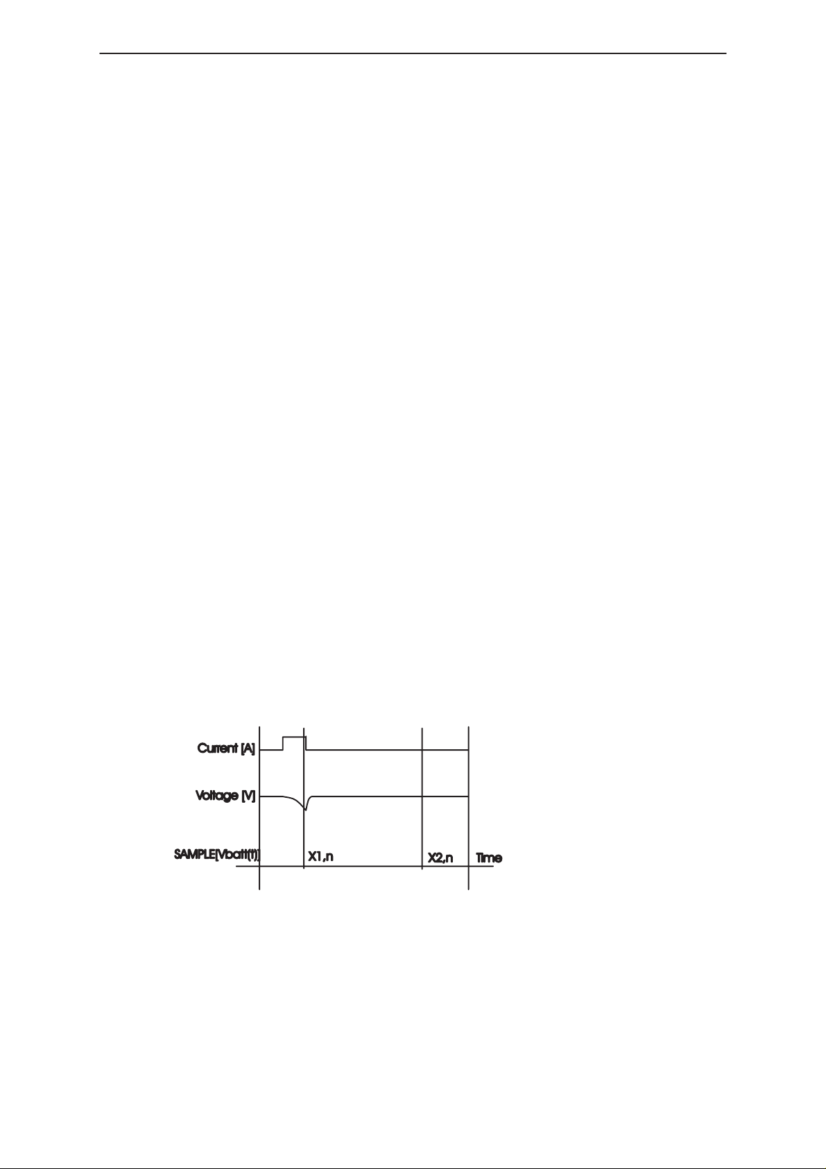
Power Off due to low Battery Voltage
The battery monitor software determines when the handset must power
off due to low battery voltage. This happens when the battery voltage,
estimated by the monitor software, reaches a predefined level, the cutoff
voltage. The cutoff voltage depends upon the battery type, in HD844 they
are 5.3V for NiMH, and 5.5V for Li–ION.
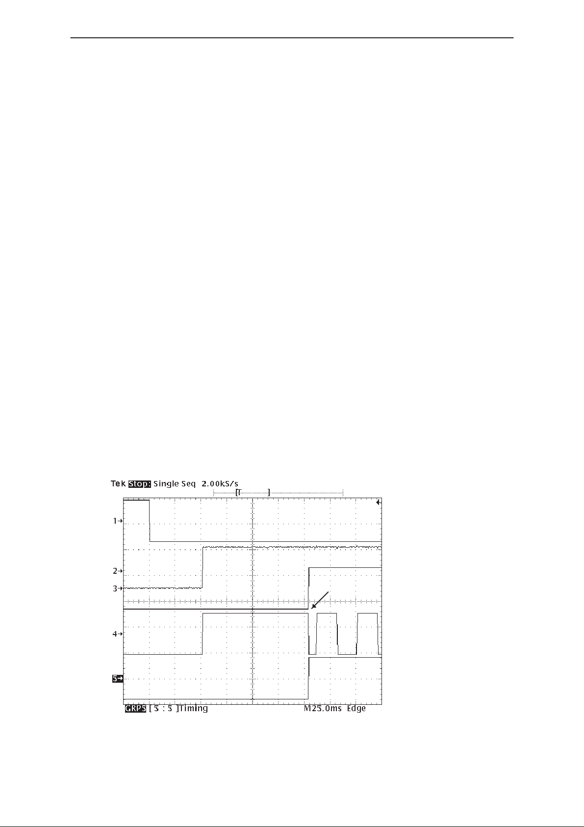
TX–on TX–off
MCU
The baseband uses a Hitachi H3001 type of MCU. This is a 16–bit internal
MCU with 8–bit external data bus. The MCU is capable of addressing up
to 16 MByte of memory space linearly depending upon the mode of
operation. The MCU has a non multiplexed address/data bus which
means that memory access can be done using less clock cycles thus
improving the performance but also tightening up memory access
requirements.
issue 3 12/98
Page 3 – 31
Page 32

NHE–8/9
System Module
The MCU is used in mode 3 which means 8–bit external data bus and 16
Mbyte of address space. The MCU operating frequency is equal to the
supplied clock frequency. The MCU has 512 bytes of internal SRAM. The
MCU has one serial channel, USART that can operate in synchronous and
asynchronous mode.
The USART is used in the MBUS implementation. Clock required for the
USART is generated by the internal baud rate generator. The MCU has 5
internal timers that can be used for timing generation. Timer TIOCA0 input
pin 71 is used for generation of netfree signal from the MBUS receive
signal which is connected to the MCU USART receiver input on pin 2.
The reason for generating the MBUS netfree using the counter is the fact
that the 32.768 kHz clock that would have been used for this timing is a
slow starting oscillator. Which means that in production testing the MBUS
can not be operated until the netfree counter is operational.
As the netfree counter is implemented using the MCU internal counter the
netfree counter is available immediately after reset. In the same way the
MCU OS timer is operated from an internal timer in the early stage until
the 32.768 kHz clock can be enabled and the OS timer provided in the
ASIC can be used.
PAMS
Technical Documentation
The MCU contains 4 10–bit A/D converters channels that are used for
baseband monitoring.
The MCU, D150 has several programmable I/O ports which can be
configured by SW. Port 4 which multiplexed with the LSB part of the data
bus is used baseband control. In the mode the MCU is operating, this port
can be used as an I/O port and not as part of the data bus, D0–D7.
MCU Access and Wait State Generation
The MCU can access external devices in 2 state access or 3 state access.
In two state access the MCU uses two clock cycles to access data from
the external device.
In 3 state access the MCU uses 3 clock cycles to access the external
device or more if wait states are enabled. The wait state controller can
operate in different modes. In this case the programmable wait mode is
used. This means that the programmed number of wait states in the wait
control register is inserted when an access is performed to a device
located in that area. The complete address space is divided into 8 areas
each covering 2 MByte of address space. The access type for each area
can be set by bits in the access state control register. Further more the
wait state function can be enabled separately for each area by the wait
state control enable register. This means that in 3 state access two types
of accesses can be performed with a fixed setting:
3 state access without wait states
If the wait state controller is not enabled for a 3 state access area no waits
states are inserted when accessing that area even if the wait control
register contains a value that differs from 0.
Page 3 – 32
3 state access with the number of wait states inserted
determined by the wait control register
issue 3 12/98
Page 33

PAMS
NHE–8/9
Technical Documentation
MCU and Memory Map
The chip selects for the memories is generated by the ASIC. MCU
address lines A23–A21 are used for this purpose. This means that the
MCU address space can be divided into 8 areas, the same amount of
areas that the MCU supports for wait state generation. For ASIC, D150
access MCU address A5–A0 is used. 7–bits are required during MCU
boot access while ASIC register access requires 6–bits. The boot ROM
and internal ASIC, D151 registers are located in separate areas to allow
the use of only 7 address bits for addressing both the boot ROM and ASIC
registers.
The MCU starts up with address lines A23–A21 configured as I/O lines
even if the operating mode is set to extended mode by HW. To avoid
address decoding problems the internal addresses for decoding the ASIC
registers are gated until the first write operation to the ASIC registers.
Before this write operation is performed, the MCU must set up address
signal A23–A21 to be used as addresses lines. The MCU IC design has
been modified in later versions to work according to mode setting pin.
The first write operation, a ”dummy” write, enables the address lines
internally in the ASIC and ASIC registers can be accessed by write
operations.
System Module
The MCU Boots from address 000000H. After D151 reset sequence this
address is located in the ASIC, D151 internal ROM, which is 128 bytes.
During the execution of this code the MCU, D150 looks if pin 3, serial
clock SCK is pulled low. In this case the execution stops and the MCU
waits for the flash prommer to initiate flash loading. If the SCK line is not
pulled low and if the flash is empty the MCU starts execution from the
flash address 40000EH.
The flash area 400000H–40000DH is reserved for baseband related HW
identifiers. This field is used to tell the MCU the configuration of the
baseband it is operating in. MCU operating speed, number of program
memories, amount of wait states, EEPROM configuration etc. is coded
into these bytes. The flash prommer specifications deals with this in more
detail. In case of SW update the flash prommer will use the same identifier
as read out at the startup of the reprogramming.
As the MCU external SRAM is mapped in the same area as the boot ROM
the MCU must write to the ASIC in order to disable the boot ROM and
enable the external SRAM. The MCU then sets up the wait state registers
and the access registers. After reset all access is performed using 3 state
access with 3 wait states inserted to allow initial boot with very slow
devices.
Since the interrupt vector table resides in the area 000004H–0000F3H the
vector table must be copied from the flash to the SRAM before any
interrupt is enabled. In case this is not done properly the SW will crash at
the point when the interrupts are to be serviced.
The ASIC is located in the address area close to the end to allow short
addressing operations to the ASIC registers to improve the performance
of the system.
issue 3 12/98
Page 3 – 33
Page 34

NHE–8/9
System Module
The flash area is divided into two areas to allow for two devices to be used
in case of availability problem or large memory requirement. nhe–8/9 uses
only one device in the first flash area.
The EEPROM area is reserved for parallel EEPROM devices. nhe–8/9 is
prepared for parallel EEPROM, but the default EEPROM is a serial device
connected to the MCU I/O port.
MCU Flash Loading
The flash loading equipment is connected to the baseband by means of
the test connector before the module is cut out from the frame. Updating
SW on a final product is done by removing the battery and connect a
special adapter that contains the necessary contacting elements. The
contacts on the baseband board are test points that are accessable when
the battery is detached. The power supply for the base band is supplied
via the adapter and controlled by the flash programming equipment. The
base band module is powered up when the power is connected to the
battery contact pins.
PAMS
Technical Documentation
The interface lines between the flash prommer and the baseband are in
low state when power is not connected by the flash prommer. The data
transfer between the flash programming equipment and the base band is
synchronous and the clock is generated by the flash prommer. The same
USART that is used for MBUS communication is used for the serial
synchronous communication. The PSCLD watchdog is disabled when the
flash loading battery pack and cable is connected.
After the flash battery pack adapter has been mounted or the test
connector has been connected to the board the power to the base band
module is connected by the flash prommer or the test equipment. All
interface lines are kept low except for the data transmit from the baseband
that is in reception mode on the flash prommer side, this signal is called
TXF. The MCU boots from ASIC and investigates the status of the
synchronous clock line.
If the clock input line from the flash prommer is low or no valid SW is
located in the flash the MCU forces the initially high TXF line low,
acknowledging to the flash prommer that it is ready to accept data . The
flash prommer sends data length, 2 bytes, on the RXF data line to the
baseband.
The MCU acknowledges the 2 data byte reception by pulling the TXF line
high. The flash prommer now transmits the data on the RXF line to the
MCU. The MCU loads the data into the internal SRAM. After having
received the transferred data correctly MCU puts the TXF line low and
jumps into internal SRAM and starts to execute the code.
Page 3 – 34
issue 3 12/98
Page 35

PAMS
NHE–8/9
Technical Documentation
After a guard time of 1 ms the TXF line is put high by the MCU. After 1
ms the TXF is put low indicating that the external SRAM test is going on.
After further 1 ms the TXF is put high indicating that external SRAM test
has passed. The MCU performs the flash memory identification based
upon the identifiers specified in the Flash Programming Specifications. In
case of an empty device, identifier locations shows FFH, the flash device
code is read and transmitted to the Flash Prommer.
Boot OK
Reset
Length OK
TXF
Ready to send
Flash ID
Internal SRAM
External SRAM
test going on
execution begin External SRAM
test passed
System Module
1 ms
Figure 5. Flash Loading acknowledgement procedure
After that, the device mounted on base band has been identified the Flash
Prommer down loads the appropriate programming algorithm to the
baseband. The algorithm is stored in the external SRAM on the baseband
module and after having down loaded the algorithm and the data transfer
SW, MCU jumps to the external SRAM and starts to execute the code.
The MCU now asks the prommer to connect the flash programming power
supply. This SW loads the data to be programmed into the flash and
implements the programming algorithm that has been down loaded. The
flash data is loaded in bytes.
Flash Prommer Connection Using Dummy Battery
For MCU SW updating in the field a special adapter can be used to
connect to the test points which are accessable through SIM opening in
the chassis, located behind the battery. Supply voltage must be connected
as well as the flash programming equipment
Flash, D400
A 8 MBit flash is used as the main program memory, D400 the device is 3
V read/program with external 12V VPP for programming. The device is
sectored and contains 16 64 kByte blocks. The sector capability is not
used in the nhe–8/9 application. The speed of the device is 180 ns. The
MCU operating at 13 MHz will access the flash in 3 state access, requiring
190 ns access time from the memory.
issue 3 12/98
Page 3 – 35
Page 36

NHE–8/9
System Module
The flash has a deep power down mode that can be used when the
device is not active. There is a requirement for a longer access time if the
device is accessed immediately after exiting power down. This
requirement is met since the signal controlling the VCO power control is
used for this purpose. The flash power down pin, pin 12 is connected to
ASIC, D151 pin 130.
The reason for connecting it to the ASIC and not direct to the VCO power
control signal is that this pin on the ASIC is low as long as the ASIC is in
reset mode. This signal resets the flash memory and acts as a power up
reset to the memory.
SRAM D403 for MCU
The baseband is designed to use SRAM size 128x8/64kx8. Default in
nhe–8/9 is 64Kx8. The required speed is 100 ns as the MCU will operate
at 13 MHz and the SRAM will be accessed in 3 state access. The SRAM
has no battery backup which means that the content is lost even during
short power supply disconnections. As shown in the memory map the
SRAM is not accessable after boot until the MCU has enabled the SRAM
access by writing to the ASIC register.
PAMS
Technical Documentation
Serial EEPROM D402
The nhe–8/9 Base Band uses 2Kx8 bit I2C serial EEPROM , which is
connected to the MCU port P4. The 16 kbit serial EEPROM has a 16 byte
page. The byte/page write time is 10 ms. The EEPROM uses I2C serial
interface to communicate with the MCU. In addition to this the EEPROM
has a write protect signal, pin 7 that protects the EEPROM from accidental
write operations, if high. The write protect signal, pin 7 must be low, before
the write operation to the EEPROM can start. After that the write operation
is completed the write enable signal is put into inactive state, high.
The MCU generates by SW the required I2C timing on the SDA (serial
data) and SCL (serial clock) pins at port P4 used for the EEPROM
interface. The device acknowledges it’s presence after each address
written to it. When writing, each byte is acknowledged. The acknowledge
procedure takes place during the ” fictive” transmission of the 9 th bit. The
MCU must therefore release the line for the 9 th bit, give the clock pulse
for the device, to perform the acknowledgement. The serial data line is
operating as open drain which requires pull up resistor on the base band.
The device has 3 external address pins. These adress pins are user
selectable. The relation between the transmitted address and the pin
setting is inverted. The device pins will be tied to ground on the base band
which means that the first 4 address bits to be put out on the data line are
”1010”, the MSB is internally fixed to ”1”. As the device is configured as
8x256 byte memory areas the next 3 bits selects the area. In this device
address byte the read/write bit is transmitted. The next byte to be output
on the data line is the word address, which gives the final byte address.
The device will acknowledge both these bytes.
Page 3 – 36
issue 3 12/98
Page 37

PAMS
NHE–8/9
Technical Documentation
Data must be valid 5 us before rising edge of the clock and the data hold
time is specified to 0 ns with respect to the falling edge. The setup time
must be implemented by the MCU SW. The hold time is simply achieved
by first writing the clock to low state and after that the status of the data
line is changed.
Note:–The page write mode is initialised by not transmitting the stop bit after each byte
transfer. The EEPROM acknowledge each byte that has been written to it by pulling the
data line low during the fictive transmission of the 9 th byte.
Baseband A/D converter Channels usage in N450 and D150
The auxiliary A/D converter channels inside RFI2, N450 are used by MCU
to measure battery voltage , reference voltage output and system board
temperature. This value is used to controll LCD operating voltage for
optimal contrast as a function of temperature.
The A/D converters are accessed by the DSP, D152 via the ASIC, D151.
The required resolution is 10 bit.
System Module
The scaling factor is created using 5% resistors and it is therefore a
requirement to have an alignment procedure in the production phase.
Each resistor network is supplied with a known input voltage and the
measured value is used against the theoretically calculated value. As a
result of this operation standard 5% resistors can be used in the voltage
scaling circuitry.
The A/D converter used in RFI2, N450 for the measurement are
sigma–delta type and the zero value is centered around 50 % of the
supply voltage, 1.6V. This means that the A/D converter reading is
negative when the input voltage to the converter is less than half of the
supply voltage. In calculations the true A/D reading is got by adding 800H
to the read value modulo 4096.
The MCU has 4 10 bit A/D channels which are used in parallel to the
channels in N450. The MCu can measure charger voltage, battery size,
battery temperature and accessory detection by using it’s own converters.
External Accessory Detection via XMIC/ID –line
MCU A/D channel 2 is used to detect accessories connected to the
system connector using the XMIC/ID line. To be able to determine which
accessory has been connected MCU measures the DC voltage on the
XMIC/ID input. The accessory is detected in accordance with the CAP
Accessory specifications. The base band has a pull–up resistor network
of 32 kohm to VA. The accessory has a pull down. The A/D converter
value can be calculated using the following formula:
A/D = (ACCI+10 kohm)/(ACCI+32 kohm)x4095x/3.2
where ACCI is the DC input impedance of the accessory device
connected to the system connector.
issue 3 12/98
Page 3 – 37
Page 38

NHE–8/9
System Module
PAMS
Technical Documentation
Table 15. Accessory Detection Voltage
Accessory
Type
IR Link 100 kohm 2.46 2.63 2.79 853
Headset 47 kohm 2.1 2.3 2.45 739
Compact HF 22 kohm 1.7 1.9 2.05 607
Accessory
resistance
Voltage on A/D Converter Channel 5
terminal (V)
Min Typ Max
A/D Con-
verter Val-
ue (Dec)
Keyboard Interface
The keypad matrix is located on a UI module PCB,intefacing is
acomplished by the board to board connector X101. The power–on key is
also connected to the PSCLD to switch power on. Due to the internal pull
up inside PSCLD, N300 to a higher battery voltage, a rectifier, V418 on
the UI board is required in the keypad matrix for the power on keypad to
prevent the higher voltage to interfere with the keypad matrix.
Series resistors, R261–R264 are implemented in the Column output to
reduce the EMI radiation to the UI PCB. Capacitors C257–C260 reduces
the EMC radiation and absorbs any ESD produced over an air gap to the
keymat.
Remark
As the serial display driver interface uses ROW5 for data transmission
series resistors are needed to prevent keypad or double keypad pressing
from interfering with the display communication. In a similar way
R265–R269 in the ROW lines reduces the EMI to the UI board. Capacitors
C251–C256 implements a LP–filter together with each resistor in the
ROW line. The capacitors also absorbs ESD pulses over an air gap to the
keymat.
During idle mode when no keyboard activity is present the MCU sets the
column outputs to ”0” and enables the keyboard interrupt. An interrupt is
generated when a ROW input is pulled low. Each ROW input on the ASIC,
D151 has an internal pull–up. The keyboard interrupt starts up the MCU,
which begins the scanning procedure. As there are keypads to be
detected outside the matrix the MCU sets all columns to ”1” and reads the
ROW inputs. If a logic ”0” is read on any ROW this means that one of the
6 possible non matrix keypads has been pressed. If the result was a ”1”
on each ROW the MCU writes a ”0” on each column consecutively while
the rest of the column outputs are kept in tri–state to allow dual keypad
activation to be detected.
After that the keyboard scanning is completed and no activity is found the
MCU writes ”0” to all columns, enables the keyboard interrupt and enters
sleep mode where the clock to the MCU is stopped. A key press will again
wake up the MCU.
Page 3 – 38
issue 3 12/98
Page 39

PAMS
NHE–8/9
Technical Documentation
Keyboard and Display Light
The display and keyboard are illuminated by LED’s. The light is normally
switched on when any key is pressed. The rules for light switching are
defined in the SW UI specifications. The display and keyboard lights are
controlled by the MCU. The LED’s are connected two in series to reduce
the power consumption. Due to the amount of LED’s required for the
keyboard and display light they are divided into three groups. Each group
has it’s own control transistor. The LED switch transistor is connected as a
constant current source, which means that the current limiting resistor is
put in the emitter circuitry. This arrangement will maintain LED brightness
over battery voltage variations and momentary power consumption of the
phone. The LED’s are connected straight to the battery voltage, to lighten
load on regulated voltages. This connection allows two LED’s to
connected in series.
The light requirement is different for the display and the keyboard. This is
one of the reason for splitting the LED control among three transistors.
Each LED group can now be set to different LED current thus affecting the
illumination. The reason for splitting the LED control is the power
dissipation in the control transistor and the current limiting resistor. This is
particular the problem during charging when the battery voltage is high.
System Module
The LED transistor control lines are coming from PSCLD. The MCU
controls these lines by writing to PSCLD using the serial control bus.
There are two LED control lines provided by the PSCLD. The display and
keyboard light controls are connected to a separate control lines. This
means that the keyboard and display light can be controlled separately.
The advantage of this is that the power dissipation and heating of the
phone can be reduced by only having the required lights switched on.
There is no PWM control on these PSCLD control lines to allow dimming
of the keyboard and display lights. These control outputs from PSCLD are
low when PSCLD exits reset mode, lights are off, and MCU then switches
them on according to the user settings or user actions.
Audio Control
The audio codec N200 is controlled by the MCU, D150. Digital audio is
transferred on the CODECB(5:0). PCM data is clocked at 512 kHz from
the ASIC and the ASIC also generates 8 kHz synchronization signal for
the bus. Data is put out on the bus at the rising edge of the clock and read
in at the falling edge. Data from the DSP, D152 to the audio codec, N200
is transmitted as a separate signal compared to data transmitted from the
audio codec, N200 to the DSP, D152.
issue 3 12/98
Page 3 – 39
Page 40

NHE–8/9
System Module
The communication is full duplex synchronous. The transmission is
started at the falling edge of the synchronization pulse. 16 bits of data is
transmitted after each synchronization pulse. The 512 kHz clock is
generated form the13 MHz ’master clock’ using a PLL type of approach
which means that the output frequency is not 512 kHz at any moment.
The frequency varies as the PLL adjusts the frequency. The average
frequency is 512 kHz.
The clock is not supplied to the codec when it is not needed. The clock is
controlled by both MCU and DSP. DTMF tones are generated by the audio
codec and for that purposes the 512 kHz clock is needed. The MCU must
switch on the clock before the DTMF generation control data is
transmitted on the serial control bus.
The serial control bus uses clock, data and chip select to communicate
with the device on the bus. This interface is built into the ASIC and the
MCU writes the destination and data to the ASIC registers. The serial
communication is then initiated by the ASIC. Data can be read form the
audio codec, N200 via this bus.
PAMS
Technical Documentation
Internal Audio
The bias for the internal microphone is generated from the PSCLD, N300
analog output, VA using a bias generator. The bias generation is designed
in such a way that common mode signals induced into the microphone
capsule wires are suppressed by the input amplifier in the audio codec.
The resistor, R209 is implented to have a well defined load of the
microphone bias transistor,V200. The bias generator is switched on/off by
the MCU to save power, when not needed, the control signal is taken from
the audio codec, N200 output latch, pin 26. The microphone amplifier gain
is set by the MCU to match with the used microphone. The microphone
amplifier input to the audio codec is a symmetrical input.
The microphone signal is connected to the baseband using filtering to
prevent EMC radiation and RF PA signal to interfere with the microphone
signal.
The microphone house is equiped with a 470pF 0603 capacitor to
suppress 900 MHz interference. R205 is connected to ground for the
microphone bias current. R202 supplies the bias current to the
microphone from the generator circuitry R201, R209, C200 and V200.
R221 and C202 in the positive microphone path forms a simple lowpass
filter, the same goes for R222 and C205 in the negative path. C203 and
C206 are used to remove the DC level from the bias circuitry, before the
microphone signal is fead to the CODEC.
The earpiece amplifier used for the internal earpiece is of differential type
and is designed as a bridge amplifier to give the output swing for the
required sound pressure. Since the power supply is only 3V a dynamic
type ear piece has to be used to achieve the propper sound pressure.
This means that the ear piece is a low impedance type and represents a
significant load to the output amplifier.
Page 3 – 40
issue 3 12/98
Page 41

PAMS
NHE–8/9
Technical Documentation
Series inductors are implemented to prevent EMC radiation from the
connection on baseband to the earpiece. The same filter also prevents the
PA RF field from causing interference in the audio codec, N200 output
stage to the earpiece.
The buzzer is controlled by the PWM output provided by the audio codec,
N200. Transistors V425 and V403 on UI board acts as drivers for the low
impedance buzzer. The buzzer is driven from the battery voltage via
V403. As the buzzer is connected to the baseband via the keyboard the
buzzer driving signal ’BUZZER’ is EMC protected in baseband module .
As the buzzer is a dynamic one the impedance shows a clear inductance.
Therefore a free running diode V413 in UI is used to clip the voltage
spikes induced in the Buzzer line when the driving transistor, V403 is
switched off.
The buzzer frequency is determined by the internal setup of N200. The
frequency is determined by the MCU via the serial control bus. The output
level can be adjusted by the PWM function in the buzzer output in N200.
External Audio
System Module
The external microphone audio signal is applied to the baseband system
connector and connected to the audio block using signals XMIC and
SGND. In order to improve the external audio performance the input
circuitry is arranged in a sort of dual ended. A wheatstone type of bridge
configuration is created by resistors R216, R217, R219 and R220. The
signal is attenuated around 20 dB to not cause distortion in the
microphone amplifier. The microphone signal is attenuated by resistors
R216, R207 and R217.
To allow the external earpiece to be driven dual ended the external
microphone signal ground is connected to the negative output of the
external audio earpiece amplifier. This means that with reference to audio
codec, N200 ground, there is a signal level on the SGND line. This
arrangement requires that the external microphone amplifier supplies the
signal on the SGND line to the XMIC line.
With this arrangement the differential voltage over R207 caused by the
signal in the SGND line is canceled. There is however a common mode
component which is relatively high presented at both the external
microphone input pins at the audio codec input, pins 31 and 30. The
microphone amplifier has a good common mode rejection ratio, but a
slight phase shift in the signals will remove the balance.
To compensate for this the signal from the external earpiece amplifier
positive output, which also feeds the external audio output from the
baseband, is feed to the remaining resistors in the bridge, R219 and
R220. This arrangement will attenuate the common mode signal
presented to the microphone amplifier caused by the audio signal in the
SGND line. Since the positive output from the audio codec, XEAR signal
introduces a DC signal to the microphone amplifier the DC signal on the
XMIC and SGND lines are blocked by capacitors C218 and C220.
issue 3 12/98
Page 3 – 41
Page 42
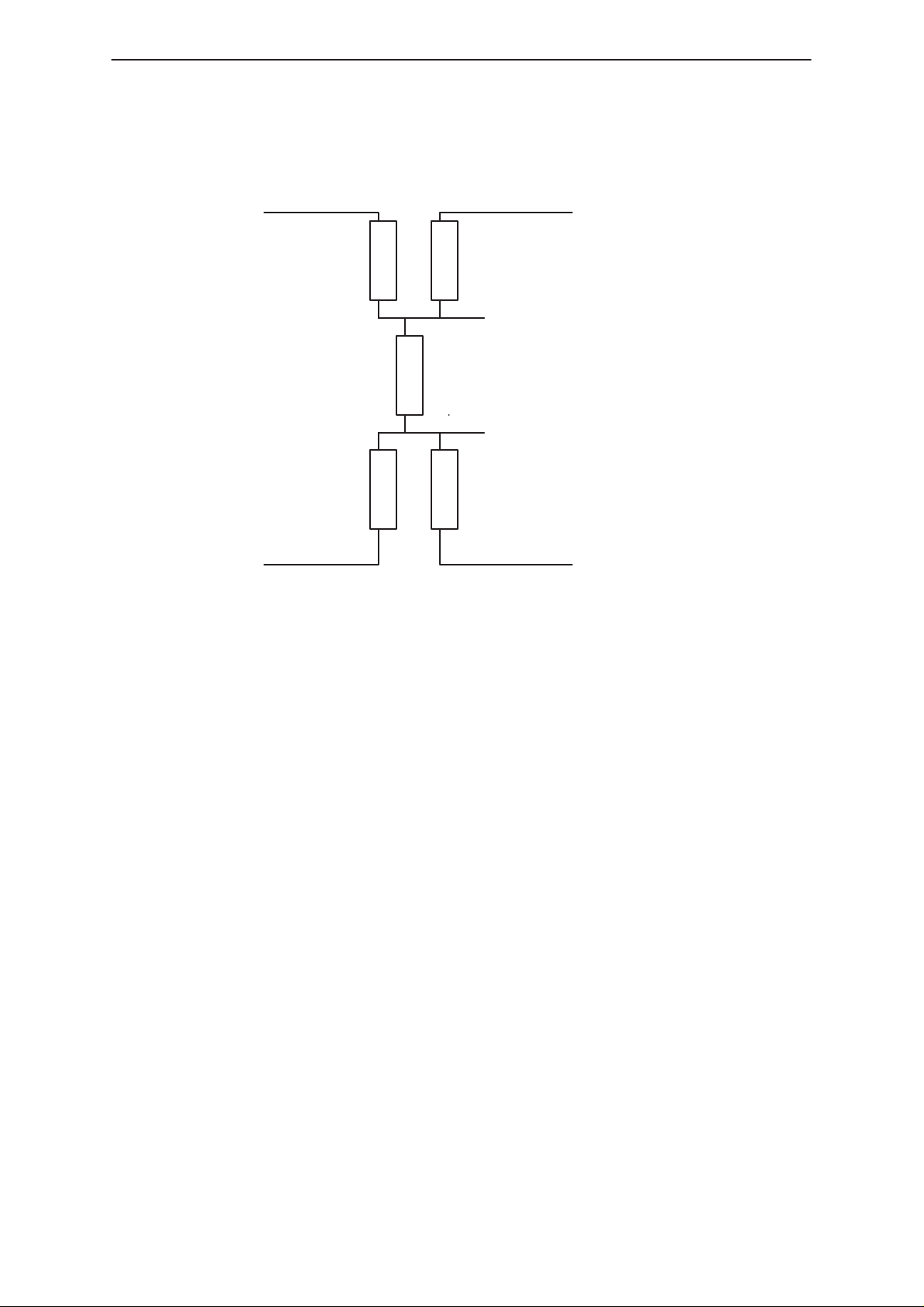
NHE–8/9
System Module
PAMS
Technical Documentation
XMIC
SGND
R216
R219
Microphone +
R207
Microphone –
R220R217
Figure 6. XMIC Bridge Implementation
XEAR
XEAR
DSP
The external audio output is the XEAR signal on the system connector
pin. The XEAR signal is taken from audio codec N200 pin 3. The output
impedance is increased to 47 ohms by resistor R214. This resistor
prevents the output amplifier from being short circuited even if the pin at
the system connector is short circuited.
The DC voltage at the XEAR output is used to control the mute function of
the accessory. When internal audio is selected the XEAR amplifier in
N200 is switched off and the DC voltage at the output on pin 2 is removed.
External audio output level is adjusted by the variable gain amplifier in the
N200 by MCU via the serial control bus from the ASIC, D151. L104 and
C102 is EMC protection for the XEAR signal at the system connector. This
filter also prevents RF signals induced in the external cables from creating
interference in the audio codec output stage.
The DSP, D152 executes code from the internal ROM. The baseband also
provides external memories for the DSP, D404 and D405. The DSP is
capable of addressing 64 kword of memory. The memory area is divided
into a code execution area and a data storage area. The code execution
area is located at address 8000H–FFFFH. The external memories are
arranged in such a way that the DSP can access the external memories
both as data storage and code execution.
Page 3 – 42
issue 3 12/98
Page 43

PAMS
NHE–8/9
Technical Documentation
The memory chip select is taken from the memory access strobe signal
from the DSP. This means that the memory is active during any memory
access. The memories are connected in such a way that the write control
is CE controlled write,which means that both the write signal and the
output enable signal are active at the same time. This implementation is
required since the DSP supports only one signal for write/read control.
The DSP is operating form the 13 MHz clock. In order to get the required
performance the frequency is internally increased by a PLL to 39 MHz.
The PLL requires a settling time of 50 us after the clock has been supplied
before proper operation is established. This settling counter is inside the
DSP although the ASIC, D151 contains a counter that will delay the
interrupt with a programmable amount of clock cycles before the interrupt
causing the clock to be switched on is presented to the DSP.
The DSP has full control over the clock supplied to it. When the DSP is to
enter sleep mode the clock is switched off by setting a bit in the ASIC
register. The clock is automatically switched on when an interrupt is
generated.
System Module
DSP ASIC Access
The DSP is accessing the ASIC in the DSP I/O area. 2 wait states are
required for the ASIC access. Some of the DSP registers located in the
ASIC are retimed to the internal ASIC clock and requires special handling
with respect to consecutive writing, which means that the same register
can not be re–written until a specified time has passed. To cope with this
DSP is inserting NOP instructions to satisfy this delay requirement.
DSP Interrupts
The DSP supports 4 external interrupts, of which 3 are used. The
interrupts to the DSP are active low.
The ASIC, D151 generates two of the interrupts. The last interrupt is
generated by the RFI2, N450 auxiliary A/D converter, to indicate a
baseband measurement A/D conversion is completed.
INT0, which is the highest priority interrupt, is used for data reception from
the receiver and is generated by the ASIC. INT1 signal is used for
auxiliary A/D channel conversions generated by the RFI2, and indicates
termination of a measurement, requested by the DSP.
There are 8 auxiliary channels supported by the RFI2, not all are used in
nhe–8/9 even though most of the channels are connected. INT3 is a low
priority interrupt generated by the ASIC timer. The DSP programs the
timer value and an interrupt is given when the timer expires. The interrupt
must be active at least 1 DSP clock cycle as it is sampled on the
rising/falling edge by the DSP.
issue 3 12/98
Page 3 – 43
Page 44

NHE–8/9
System Module
INT0 is used for the reveiver A/D converter in RFI2. The ASIC reads the
data from the receiver path A/D converter in RFI2 at every data available
signal activation from the RFI2. After the data transfer when the data is
stored in the ASIC the ASIC generates a receiver interrupt to the DSP
using INT1 (INT0?) signal. The DSP enters the interrupt routine and
services the interrupt by reading the data from the ASIC.
INT1 signal is used for the auxiliary A/D converter channels in RFI2.
These A/D channles are used for baseband battery voltage and system
board temperature monitoring . Two channels are used for battery
monitoring. The start of the A/D conversion task is timed in such a way
that auxiliary channel 0 results are measured during transmission when
the PA is active and channel 7 is measuring when the PA is off.
DSP Serial Communications Interface
The DSP contains two synchronous serial communications interfaces.
One of the interfaces are used to communicate with the audio codec,
N200. The 512 kHz clock required for the data transfer is provided by the
ASIC, D151 as well as the 8 kHz synchronization signal. Data is
transferred on to lines, RX and TX creating a full duplex connection. Data
is presented on the bus on the first rising edge of the clock after the falling
edge of the synchronization pulse. Data is read in by each device on the
falling edge of clock. Data transfer is 16 bits after each synchronization
pulse.
PAMS
Technical Documentation
The DSP, D152 has control over the clock provided to the audio codec.
The DSP can switch on the clock to start the communication, and switch it
off when it is not needed. This clock is also under control of MCU, D150.
The second serial interface is used for debugging and Digital Audio
Interface. The ASIC provides the clock and the synchronization for this
serial interface as well, since the two serial interfaces need to be operated
synchronously in case of DAI measurements.
RF Synthesizer Control
The synthesizer control is performed by the DSP, D152 using the ASIC,
D151 as the interfacing and timing device. Different synthesizer interfaces
are supported, and the required interafce can be selected by the DSP at
the initialisation stage of the ASIC. The synthesizer interface also includes
timing registers for programming synthesizer data. The DSP loads the
synthesizer data into the transmission registers in the ASIC synthesizer
interface together with the timing information. The system timing
information is used for synthesizer data loading.
When the system timing register content, frame counter value, matches
the timing value programmed into the synthesizer interface, the interface
transmits the loaded data to the RF synthesizer, and the VCO frequency is
changed accordingly. As the synthesizer may be powered off, when not
needed, the interface pins towards the synthesizer can be put in tri–state
or forced low, when the interface is not active.
Page 3 – 44
issue 3 12/98
Page 45

PAMS
NHE–8/9
Technical Documentation
RFI2, N450 Operation
The RFI2, N450 contains the converters to perform the A/D conversion of
the received signal, and the D/A converters to perform the conversion of
the modulated signal to be supplied to the transmitter section. In addition
to this the RFI2 chip also contains the D/A converter for providing AFC
voltage to the RF section. This AFC voltage controls the frequency of the
13 MHz VCO which supplies the system clock to the baseband.
Additionally the RFI2, N450 also contains the D/A converter to control the
RF transmitter power control. The power control values are stored in the
ASIC, D151 and at the start of each transmission the values are read from
the ASIC, D151 to the D/A converter producing the power control pulse.
This D/A converter is used during the reception to provide AGC for the
receiver RF parts.
One of the A/D converters used for receiver signal conversion can be
used as an auxiliary converter that supplies 8 channels for baseband
measurement purposes. When the converter is used in this mode each
conversion generates an interrupt directly to the DSP. The DSP operates
this converter via the ASIC, D151.
System Module
Data communication between the ASIC, D151 and RFI2, N450 is carried
out on a 12 bit parallel data bus. The ASIC, D151 uses 4 address lines to
access RFI2, N450. Depending on the direction of the communication
either the write control signal is used to write data to RFI2, N450 or the
read signal is used to read data from RFI2, N450. The ASIC, D151
supplies 13 MHz clock to the RFI2, N450. This clock is used as reference
for the A/D and D/A converters. Communication between the ASIC, D151
and the RFI2, N450 is related to the clock.
The RFI2, N450 digital supply is taken from the baseband main digital
supply. The analog power supply, 4.5V is generated by a regulator N451
supplied from the VBATT voltage. The analog power supply is always
supplied as long as the baseband is powered and VXOENA signal is
activated ( high).
Receiver Timing and AGC
RF receiver power on timing is performed by the ASIC, D151. The DSP,
D152, can program the time when the receiver is to be powered on. The
timing information is taken from the system timing that is based upon the
frame counter inside the ASIC, D151 which is synchronised to the base
station carrier frequency using AFC to tune the receiver.
As transmission and reception takes place at different time the D/A
converter used for transmitter power control is used to control the AGC of
the receiver during reception. This requires the DSP, D152 to alter the
content of the SRAM containing the information that is written to the D/A
converter for the reception and the transmission.
issue 3 12/98
Page 3 – 45
Page 46

NHE–8/9
System Module
RF Transmitter Timing and Power Control
The RF Power Amplifier (PA) timing control is performed by the ASIC,
D151. The power control is performed by the ASIC D151 using the D/A
converter in N450. The ASIC, D151 controls the power supply voltage to
the RF transmitter sections. As the first step the relevant circuits are
powered on using the TX power control output from the ASIC, D151. The
timing for powering on the TX circuits is generated from the ASIC internal
system timing circuitry, frame counter. As the RF TX circuitry needs time
to stabilize after power on before the actual transmitter can be started
there is a programmable delay before the ASIC, D151 starts to write the
power ramp data to the D/A converter inside N450.
The TXC signal which is generated in this way controls the power ramp of
the PA and the power level for that burst. At the end of the burst the power
ramp is written to the D/A converter inside N450. The data that creates the
power ramp and final power level is stored in a SRAM inside the ASIC,
D151. At the start of the ramp the contents of the SRAM is read out in
increasing address order.
PAMS
Technical Documentation
At the end of the ramp the contents is read out in decreasing adress
order. The power level during the burst is determined by the last value in
the SRAM, this value is the value that will remain in the D/A converter
during the burst. The DSP, D152 may change the shape of the falling
slope of the power ramp by writing new values to the power ramp SRAM
during the burst.
As the transmitter may have to adjust the transmitter burst due to the
distance from the base station there is an additional timer for this purpose.
This timing is called the timing advance and will cause the transmission to
start earlier when the distance to the base station increases.
SIM Interface
The SIM interface is the serial interface between the smart card and the
baseband. The SIM interface logic levels are 5V. The baseband is
designed in such a way that a 3V technology SIM can be used whenever
it is available. The SIM interface signals are generated inside the ASIC.
The signals coming from the ASIC are converted to 5V levels. The PSCLD
circuit is used as the logic voltage conversion circuit for the SIM interface.
The PSCLD circuit also contains the voltage regulator for the SIM power
supply.
The control signals from the ASIC to PSCLD are at 3V level and the
signals between PSCLD and the SIM are 5V levels. An additional control
line between the ASIC and the PSCLD is used to control the direction of
the DATA buffer between the SIM and the PSCLD. In a 3V technology
environment this signal is internal to the ASIC only. The pull up resistor
required on the SIM DATA line is integrated into the PSCLD and the
pull–up is connected to the SIM regulator output inside PSCLD. In idle the
DATA line is kept as input by both the SIM and the interface on the base
band. The pull–up resistor is keeping the DATA line in it’s high state.
Page 3 – 46
issue 3 12/98
Page 47

PAMS
NHE–8/9
Technical Documentation
The power up and power down sequences of the SIM interface is
performed according to ISO 7816–3. To protect the card from damage
when the power supply is removed during power on there is a control
signal, CARDDETX, that automatically starts the power down sequence.
The CARDDETX information is taken from the battery size indicator
signal, BSI, from the battery connector. The battery connector is
mechanically designed in such a way that the BSI signal contact is
disconnected first, while the power is still supplied by the battery, and the
battery power contacts are disconnected after that the battery pack has
moved a specified distance.
Since the power supply to the SIM is derived from PSCLD also using 3V
technology SIM the power supply voltage of the SIM regulator is
programmable 3.15/4.8 V. The voltage is selected by using the serial
control bus to PSCLD. The default value is set to 3.2V nominal.
For cross compatibility reasons the interface should always be started up
using 3V. The 3V technology SIM will operate at 5V but a 5V SIM will not
operate at 3V. The supply voltage is switched to 5V if the SIM can accept
that. The SIM has a bit set in a data field indicating it’s capability of 3V
operation.
System Module
The DATA signal between the SIM and the PSCLD can be set to operate
in two different modes. One mode causes the PSCLD output to force a
logic high level on the DATA line when the interface is driving a high level.
In this mode the interface output is driving the DATA line actively. In the
other mode the DATA line is operating like an open drain circuitry with the
difference that during the transition periods high–low, low–high the
interface is actively forcing the DATA line.
The advantage of this is that the DATA line is acting like an open drain,
tri–state, data line but there is no problem with rise times since the data
line is actively forced during the transition period. This mode is introduced
to cope with data line overshoots that has been discovered during type
approval testing. The present solution is to force the data line actively
during the byte transmission. In the new mode the data line is not forced
actively when the data to be transmitted is high.
The regulator control signal is derived from the ASIC and this signal
controls the operation of the SIM power supply regulator inside PSCLD.
To ensure that the powered off ASIC doesn’t cause any uncontrolled
operations at the SIM interface the PSCLD signals to the SIM are forced
low when the PURX signal is active, low. This implementation will ensure
that the SIM interface can not be activated by any external signal when
PSCLD has PURX active. When PURX goes inactive the control of the
interface signals are given back to the ASIC signals controlling PSCLD
SIM interface operations.
issue 3 12/98
Page 3 – 47
Page 48

NHE–8/9
System Module
The clock to the SIM can be switched off if the SIM card allows stopping of
the clock. The clock can be stopped either in high or low state, determined
by the card data. For cards not allowing the clock to be stopped there is a
1.083 MHz clock frequency that can be used to reduce the power
consumption while the clock is running. In this case the VCO must be
running all the time.
When the clock is stopped and the status of the CARDIN signal changes,
battery is removed, the clock to the SIM is restarted inside the ASIC and
the SIM power down sequence is performed.
To be able to handle current spikes as specified in the SIM interface
specifications the SIM regulator output from PSCLD must have a ceramic
capacitor off 100 nF connected between the output and ground close to
the SIM interface connector. To be able to cope with the fall time
requirements and the disconnected contact measurements in type
approval the regulator output must be actively pulled down when the
regulator is switched off. This active pull–down must work as long as the
external battery is connected and the battery voltage is above the PSCLD
reset level.
PAMS
Technical Documentation
The SIM power on procedure is controlled by the MCU. The MCU can
power up the SIM only if the CARDDETX signal is in the inactive state.
Once the power up procedure has been started the ASIC takes care of
that the power up procedure is performed according to ISO 7816–3.
The SIM interface uses two clock frequencies 3.25 MHz or 1.625 MHz
during SIM communication. A 1.083 MHz clock is used during SIM sleep
state if the clock is not allowed to be switched off. The data transfer speed
in the SIM GSM session is specified to be the supplied clock
frequency/372. The ASIC SIM interface supplies all the required clock
frequencies as well as the required clock frequency for the UART used in
the SIM interface data transmission/reception.
SIM Interface and support in D151
The signal from the BSI input from the battery is fed to D151, pin 25. This
pin has a special input cell that has specific input levels to convert the BSI
signal into the card detection logical control signal for the SIM interface in
the ASIC. When the input voltage has been low, less than 1.5V the output
from the cell will remain low until the input voltage exceeds 2.3V.
If the input voltage has been more than 2.8V the input will remain high
until the input voltage has decreased to at least 1.9V. For all specified
battery types the BSI voltage will stay below 2.3V. If the voltage on this pin
exceeds 2.3V the card detection signal will be active and the card will be
powered down. It is not possible to power up the card as long as the card
detection signal is active, high.
Page 3 – 48
issue 3 12/98
Page 49

PAMS
NHE–8/9
Technical Documentation
Display Driver Interface
The display driver used in nhe–8/9 is Seiko SED1560DEB, located in UI
board. The display driver has internal voltage tripler circuitry for LCD
voltage generation. Capacitors C409 and C420 are used in the voltage
converter. Capacitor C 404 is the filtering capacitor for the voltage
generator output. Capacitors C400–C403 and C421 are filtering
capacitors for the supply voltage to the display driver back plane voltages.
Resistor network R416–419 forms the feedback network for setting the
contrast for the display. The display driver has internal temperature
compensation for the contrast.
The nhe–8/9 Base Band uses a serial interface to the Seiko LCD driver.
The serial interface is designed in the ASIC. The MCU writes data into the
serial interface in the ASIC and it is then transmitted to the LCD driver.
The LCD driver reset is controlled by the MCU on P40. The display driver
reset is dual edge active. The P40 pin on the MCU has a pull down
capacitor, C154 to ensure that the LCD driver reset is low at power up.
After exiting reset one of the first tasks for the MCU is to set the P40 to
output and low, ”0”. After at least 100 us the reset signal to the display
driver is taken high, ”1”. This rising edge reset selects 80XX type MCU
interface. The serial interface setting of the driver will override this. After
resetting the display driver the MCU starts the initialization procedure
using the serial interface in the ASIC, D151.
System Module
The MCU first sets up the display driver interface in the ASIC for the
serial driver. This enables the interface signals and sets the polarity of the
chip select to the driver correct. The next step is to blank the display. This
is to be done soon after the power up sequence to ensure that no garbage
is output on the display. The normal display test pattern is then written to
the display.
Communication with the serial driver takes place on the SCONB(5:0). The
display driver requires serial data, serial clock and command/display
information during the serial transfer. The display driver has it’s own chip
select which is active during the transfer, there are other devices on the
same serial bus as well. The command/display information is transmitted
on the keyboard ROW5 output. Due to the fact that the keyboard interface
is used during display driver transfers the keyboard activities must be
disabled during display driver communication. This means that the column
output from the ASIC must be put in high impedance state not to interfere
with the data transmission if keypads are pressed.
The timing required for the serial interface is provided by the ASIC and the
operation of ROW5 depends upon the display driver interface initialization.
For the serial interface it is used for command/display data control. The
serial clock is 1.083 MHz.
issue 3 12/98
Page 3 – 49
Page 50

NHE–8/9
System Module
The serial interface in the ASIC starts the transfer after each write
operation to the output buffer. The data transferred is command or data
depending upon to which address it is written in the interface. The ASIC
sets the control signal on ROW5 accordingly. After that the data has been
shifted out from the interface a bit is set in the interface register to tell the
MCU that the interface is ready for the next byte. This transmission
indicator bit is polled by the MCU and the next byte is written when the
output buffer is empty.
The clock to the display driver interface in the ASIC is automatically
switched on when a write operation to the interface has taken place. The
MCU can force the clock to be continuously on by writing the clock on to
the CTSI block. The default assumption is that the MCU forces the clock
to be continuously on only when a large amount of data is to be
transmitted, such as segment test at power up.
PAMS
Technical Documentation
Page 3 – 50
issue 3 12/98
Page 51

PAMS
NHE–8/9
Technical Documentation
RF Module
Technical Summary
The GJ3 is the RF module of the NHE–8–9 cellular transceiver, it is a
slightly modified version of the GJ8 module used in HD843. The GJ3
module carries out all the RF and system functions of the transceiver. This
module works in the GSM system.
Components are located on both sides of the PWB. The RF components
are located on the top end of the PWB. The both sides of the board
includes high and low components.
EMI leakage is prevented by a metallized plastic shield A on side 1/8
and a meatallized plastic cover B on side 8/8. The shield A also conducts
the heat out of the inner parts of the phone, thus preventing excessive
temperature rise.
System Module
External Signals and Connections
Table 16. List of RF connectors
Connector Name Code Notes
Antenna contact clip 9510262 For fixed helix antenna
Main Technical Specifications
Table 17. Main technical specifications
Item Specification
Receiver frequency band 935 ... 960 MHz
Transmitter frequency band 890 ... 915 MHz
Duplex spacing 45 MHz
Number of RF channels 124
Power class 4
Maximum output power 2.0 W (33 dBm)
Number of power levels 11 (phase I) / 15 (phase II)
Maximum Ratings
The maximum battery voltage should not exceed 9.5 V. Higher battery
voltages may destroy the tantalum capacitors. The transmitter has a
regulator circuit, which protects the power amplifier for the higher
voltages.
issue 3 12/98
Page 3 – 51
Page 52

NHE–8/9
System Module
Table 18. Maximum ratings
Parameter Value
Battery voltage 9.5 V
Power amplifier supply voltage 7.5 V
Operating temperature range –20 ... +85 deg.C
Power Distribution
All currents in the power distribution diagram are peak currents. Activity
percentages in SPEECH mode are 22.5 % for RXPWR , 15.8 % for
TXPWR and 100 % for SYNTHPWR. In the IDLE mode, activities are
0.36 %, 0.0 % and 1.61 %, respectively. The operation of each block is
controlled independently and for example TXPWR and RXPWR are not
on at the same time.
PAMS
Technical Documentation
VXOENA
SYNTHPWR
Battery
5.4...9.5 V
Regulator
4.8 V
1.5 mA
VCTCXO
37 mA 17 mA 37 mA
UHF PLL
VHF PLL
LO buffer
RX LNA
IF amplifier
Regulator
4.8 V
TX buffer
Power control
Figure 7. Power distribution diagram
Regulator
4.8 V
CRFRT
38 mA34 mA
Power amplifier
TXPWR
RXPWR
1200mA (peak)
200mA average
TXP
Regulators
There are three regulators in the RF unit. The 1st regulator is used for the
synthesizers and the VCTCXO. The 2nd regulator is used for the receiver
and the transmitter discrete circuits. The 3rd regulator is for the CRFRT,
integrated RF circuit. The regulators regulate the battery voltage to the
fixed 4.8 V level. The receiver, synthesizer and transmitter circuits can be
switched ON and OFF separately. Switching sequence timing depends
on the operation mode of the phone.
Page 3 – 52
issue 3 12/98
Page 53

PAMS
NHE–8/9
Technical Documentation
System Module
Control Signals
In the following table RF current consumption can be seen with different
status of the control signals.
Table 19. Control Signals and Current Consumption
VXOENA SYNTHPWR RXPWR TXPWR TXP Typical
load current / mA
L L L
H L L
H H L L L 37 Synthesizers
H H H L L 90 Reception
H H L H L 110 TX active
H H L H H 1100 Transmission
L L 0.05 Leakage cur-
L L 1.5 VCTCXO cur-
Notes
rent
rent
active
Table 20. Output power
Parameter Minimum Typical /
Target
Max. output power 33.0 dBm
Max. output power tolerance
(power level 5)
Output power tolerance /
power levels 6...15
Output power tolerance /
power levels 16...19 (phase
II)
Output power control step
size
0.5 2.0 3.5 dB
Maximum Unit / Notes
+/– 2.0
+/– 2.5
+/– 3.0
+/– 4.0
+/– 5.0
+/– 6.0
dB, normal cond.
dB, extreme cond.
dB, normal cond.
dB, extreme cond.
dB, normal cond.
dB, extreme cond.
issue 3 12/98
Page 3 – 53
Page 54

Page 3 – 54
EXT . ANTENNA
PDATA0
Functional Description
NHE–8/9
System Module
issue 3 12/98
Figure 8. Block Diagram
RFO_CONT
POW
DET
PA
REGU
VBAT
935–960 MHz
+
–
890–915 MHz
71 MHz
SDATA
SENA1
SCLK
UHF
VHF
PLL
PLL
UHF
VCO
RX/TX : 1006...1031 MHz 232 MHz
VHF
VCO
AFC
RFC
VCTCXO
13 MHz
116 MHz
f / 2
+
–
13 MHz
f / 2
f / 2
CRFRT
TXC
(AGC)
RXP
RXN
TXIP
TXIN
TXQP
TXQN
TXC
TXP
Technical Documentation
PAMS
Page 55

PAMS
NHE–8/9
Technical Documentation
Receiver
The SW controlled electrical switch connects the signal from the antenna
(transceiver antenna or external) to the duplex filter, which rejects the
unwanted signals. The received signal is amplified by a discrete low noise
preamplifier. The gain of the amplifier is controlled by the AGC control line
(PDATA0). The nominal gain of 20 dB is reduced in strong field
conditions by about 40 dB. After the preamplifier the signal is filtered by
the SAW RF filter. The filter rejects spurious signals coming from the
antenna and spurious emissions coming from the receiver unit.
The filtered signal is down converted by the single balanced diode mixer.
The first IF is 71 MHz. The first local signal is generated by the UHF
synthesizer.
The amplified IF signal is filtered by the SAW IF filter. The filter rejects the
adjacent channel signal, intermodulating signals and the second IF image
signal. After filtering, the IF signal is fed to the receiver ASIC (CRFRT),
which includes the AGC amplifier and the 2nd mixer. The 2nd local signal
is generated in the RF ASIC by dividing the VHF signal by four. After
mixing the 2nd IF signal is filtered by the SMD 13 MHz ceramic filter and
amplified by the differential amplifier of the ASIC. The differential 13 MHz
signal is fed through the attenuator circuit to the RF interface circuit RFI2.
System Module
Frequency Synthesizers
The stable frequency source for the synthesizers and baseband circuits is
the voltage controlled temperature compensated crystal oscillator,
VCTCXO. The frequency of the VCTCXO is 13 MHz. The frequency of
the oscillator is controlled by an AFC voltage, which is generated by the
baseband circuits.
The operating frequency range of the UHF synthesizer is from 1006 to
1031 MHz. The UHF signal source is the VCO module. The UHF PLL
locks the signal for the accurate frequency and it is used as the down
conversion signal for the receiver and the up conversion signal for the
transmitter.
The operating frequency of the VHF synthesizer is 232 MHz. This signal
is fed to the RF ASIC (CRFRT), where it is used for the I/Q modulation
and for the down conversion of the first IF. This 232 MHz signal is divided
by four inside the CRFRT before using it as a local signal for the mixer.
Transmitter
The synthesized 232 MHz signal is divided by two in the I/Q modulator of
the CRFRT. The TX I and Q signals are generated in the RFI2 interface
circuit and they are fed differentially to the modulator. The modulated TX
IF signal (116 MHz) is amplified by an AGC amplifier. In this application
the gain has been set to the maximum level, because the power control
has been implemented by the power ampllifier.
issue 3 12/98
Page 3 – 55
Page 56

NHE–8/9
System Module
The TX signal is generated by mixing the UHF VCO signal and the
modulated TX IF signal. After mixing the slightly filtered TX signal is
amplified by the power amplifier to the level of +5 dBm. The unwanted
signals are filtered by the SAW RF filter.
The power amplifier module amplifies the TX signal to the used power
level. The maximum output level of the amplifier is 36 dBm, typically.
The power control loop controls the output level of the power amplifier
module. The power detector consists of a directional coupler and a diode
rectifier. The difference of the power control signal TXGX (TXC amplified
in CRFRT) and the detected voltage is amplified and used as a control
voltage for the power amplifier,
The duplex filter rejects the noise on the receiver band and the harmonic
products of the TX signals. The electrical switch connects the signal to
the used antenna.
PAMS
Technical Documentation
Receiver Characteristics
Table 21. RF Characteristics, Receiver
Item Values
RX frequency range 935 ... 960 MHz
Type Linear, two IFs
Intermediate frequencies 71 MHz, 13 MHz
3 dB bandwidth +/– 100 kHz
Reference noise bandwidth 270 kHz
Sensitivity –102 dBm, S/N ratio > 8 dB, BN=135 kHz
AGC dynamic range 94 dB, typ.
Receiver gain 65 dB (voltage gain)
RF front end gain control range 40 dB
2nd IF gain control range 57 dB
Input dynamic range –102 ... –10 dBm
Gain relative accuracy in receiving band +/– 1.5 dB
Gain relative accuracy on channel +/– 0.4 dB
Duplex filter
The duplex filter combines the transmitter and the receiver to the antenna
connection. The TX filter rejects the noise power at the RX frequency
band and TX harmonic signals. The RX filter rejects blocking and
spurious signals coming from the antenna and also protects the receiver
of the transmitter power.
Page 3 – 56
issue 3 12/98
Page 57

PAMS
NHE–8/9
Technical Documentation
Pre–amplifier
The pre–amplifier amplifies the received signal. The performance of the
amplifier determines the sensitivity of the receiver.
Table 22. Pre amplifier specifications
Parameter Minimum Typical /
Nominal
Frequency band 935...960 MHz
Supply voltage 4.5 4.8 V
Current consumption 7.0 mA
Insertion gain 16 18 dB
Noise figure 2.5 dB
Reverse isolation 15 dB
Gain reduction (PDATA0=1) 40 dB
IIP3 –10 dBm
Input VSWR (Zo=50 ohms) 2.0
Maximum Unit / Notes
System Module
Output VSWR (Zo=50 ohms) 2.0
RX Interstage Filter
The RX interstage filter is an SAW filter. The filter rejects spurious and
blocking signals coming from the antenna and also rejects the local
oscillator signal leakage.
Table 23. RX filter specification
Parameter Minimum Typical /
Nominal
Terminating impedance 50 ohms
Operating temperature range –25 +80 deg. C
Center frequency (fo) 947.5 MHz
Bandwidth (BW) +/– 12.5 MHz
Insertion loss at BW 4.0 dB
Ripple at BW 1.5 dB
Return loss at BW 10.0 dB
Attenuation DC ... 890 MHz 35.0 dB
Attenuation 890 ... 915 MHz 20.0 dB
Maximum Unit / Notes
Attenuation 980 ... 1025 MHz 15.0 dB
Attenuation 1025 ... 1500
MHz
35.0 dB
issue 3 12/98
Page 3 – 57
Page 58
NHE–8/9
System Module
Diode mixer
The first mixer is a single balanced diode mixer. The mixer consists of a
microstripline balun and a ring quad schottky diode. One diode pair is
used for the receiver and the other is used for up conversion of the
transmitter signal.
PAMS
Technical Documentation
Table 24. Mixer specifications
Parameter Minimum Typical /
Nominal
RX frequency range 935 960 MHz
LO frequency range 1006 1031 MHz
IF frequency 71 MHz
Conversion loss 7.0 9.0 dB
IIP3 5.0 dBm
LO – RF isolation 15.0 dB
LO power level 3.0 dBm
Maximum Unit / Notes
IF amplifier
The first IF bipolar transistor amplifier drives up the level of the down
converted signal before filtering.
Table 25. IF amplifier specifications
Parameter Minimum Typical /
Nominal
Opertion frequency 71 MHz
Supply voltage 4.5 4.8 V
Maximum Unit / Notes
Current consumption 12.0 mA
Insertion gain 19 20 dB
Noise figure 3.0 dB
IIP3 –5.0 dBm
First IF filter
The first IF filter makes the part of the channel selectivity of the receiver.
It rejects adjacent channel signals (except the 2nd adjacent). It also
rejects blocking signals and the 2nd image frequency.
Table 26. IF filter specifications
Parameter Minimum Typical /
Nominal
Center frequency, fo 71.0 MHz
Operating temperature range –20 ... +80 deg.C
Input impedance 3.5 kohm // 6.9 pF balanced
Output impedance 3.4 kohm // 6.7 pF balanced
Insertion loss 11.5 13.5 dB
Maximum Unit / Notes
Page 3 – 58
issue 3 12/98
Page 59

PAMS
NHE–8/9
Technical Documentation
Table 26. IF filter specifications (continued)
MinimumParameter
Nominal
Group delay distortion 700 1300 ns
2 dB bandwidth +/– 80 kHz
3 dB bandwidth +/– 120 kHz
5 dB bandwidth +/– 230 kHz
20 dB bandwidth +/– 400 kHz
30 dB bandwidth +/– 600 kHz
35 dB bandwidth +/– 800 kHz
Spurious rejection at
fo +/– 26 MHz
60 dB
Receiver IF circuit, RX part of CRFRT
The receiver part of CRFRT consists of an AGC amplifier, a mixer and a
buffer amplifier for the second IF. The mixer circuit down converts the
received signal to the 13 MHz IF frequency. After second IF filter the
signal is amplified and fed to baseband circuitry. The supply current can
be switched OFF by an external switch.
System Module
Unit / NotesMaximumTypical /
Table 27. CRFRT RX part specification
Parameter Minimum Typical /
Nominal
Supply voltage 4.27 4.5 4.73 V
Supply current 38 mA
Input frequency range 45 87 MHz,
Max voltage gain before 2IF
filt
Min voltage gain before 2IF
filt
AGC gain control slope 40 84 120 dB / V
Absolute gain inaccuracy –4 4 dB over temp.
Relative gain inaccuracy 0.8 dB over temp.
Noise figure 15 dB, Max gain
Mixer output 1dB comp point 1.0 Vpp
Second IF range 2 17 MHz
Gain of the 2nd IF buffer 30 dB
47 dB
–10 dB
Maximum Unit / Notes
range
range
Max output level after 2nd IF
buffer
issue 3 12/98
1.6 Vpp
Page 3 – 59
Page 60

NHE–8/9
System Module
Second IF filter
The second IF is filtered by the ceramic filter, which makes the part of the
channel selectivity of the receiver.
PAMS
Technical Documentation
Table 28. 2nd IF filter Specifications
Parameter Minimum Typical /
Nominal
Center frequency (fo) 13.0 MHz
1 dB bandwidth (BW) +/– 90 kHz
5 dB bandwidth +/– 220 kHz
Insertion loss 6.0 dB
Group delay distortion 1500 ns at BW
Attenuation: fo +/– 400 kHz 25.0 30.0 dB
Attenuation: fo +/– 600 kHz 40.0 45.0 dB
Terminating impedance 330 ohms,
Operating temperature range –30 +85 deg. C
Maximum Unit / Notes
Transmitter Characteristics
Table 29. RF Characteristics, Transmitter
Item Values
TX frequency range 890 ... 915 MHz
Type Up conversion
Intermediate frequency 116 MHz
Maximum output power 2 W (33 dBm)
Power control range 20 dB (phase I) / 28 dB (phase II)
Maximum RMS phase error 5 deg.
Maximum peak phase error 20 deg.
Modulator Circuit, TX part of the CRFRT
The modulator of the CRFRT is a quadrature modulator. The input local
signal (232 MHz) is divided by two to get accurate 90 degrees phase
shifted signals for the I/Q mixer. After mixing the signals are combined
and amplified. The output of the IC is single ended and the level is
controllable. The maximum output level is 0 dBm, typically.
Page 3 – 60
issue 3 12/98
Page 61

PAMS
NHE–8/9
Technical Documentation
Table 30. Electrical specifications, CRFRT TX section
Parameter Minimum Typical /
Nominal
Supply voltage 4.27 4.73 V
Supply current 35 mA, norm. opera-
Transmit Frequency Input Minimum Typical /
Nominal
LO input frequency 170 400 MHz
LO input power level –20 –10 0 dBm
LO input impedance 70 100 130 ohm
Modulator Inputs (I/Q) Minimum Typical /
Nominal
Input bias current 100 nA
External DC reference 2.1 2.6 V
Differential input swing 0.5 0.8 1.1 Vpp
Maximum Unit / Notes
Maximum Unit / Notes
Maximum Unit / Notes
System Module
tion
Differential input offset voltage
Input impedance 200 kohms
Gain unbalance –0.5 0.5 dB
Modulator Output Minimum Typical /
Available RF power –45.0 0.0 dBm, ZiL= 50
Suppression of 3rd order
prods
Carrier suppression 35 dB
Noise floor at saturated Pout –125 dBm/Hz
0 1.0 3.0 mV
Maximum Unit / Notes
Nominal
ohms
–35 dB, Pout = –13
dBm
Up conversion mixer
The mixer is a single balanced diode mixer. The mixer circuit is the same
as used in the receiver. The input signal is a modulated 116 MHz signal
coming from the quadrature modulator (part of the CRFRT circuit). The
TX signal is filtered by using a microstripline trap for the LO signal before
amplification.
Table 31. Mixer Specification
Parameter Minimum Typical /
Nominal
Input frequency 116 MHz
LO frequency range 1006 1031 MHz
TX frequency range 890 915 MHz
Conversion loss 7.0 8.0 dB
Maximum Unit / Notes
issue 3 12/98
Page 3 – 61
Page 62
NHE–8/9
System Module
PAMS
Technical Documentation
Table 31. Mixer Specification (continued)
MinimumParameter
Nominal
IIP3 –5.0 dBm
LO – RF isolation 20.0 dB
LO power level 3.0 dBm
TX amplifier
The TX amplifier is a bipolar MMIC amplifier. It amplifies the up converted
TX signal to the level required by the power amplifier.
Table 32. TX amplifier specification
Parameter Minimum Typical /
Nominal
Operation frequency range 890 915 MHz
Supply voltage 4.5 V
Current consumption 28.0 mA
Insertion gain 20.0 dB
Output power 5.0 dBm
Noise figure 4.0 dB
Maximum Unit / Notes
Unit / NotesMaximumTypical /
Input VSWR (Zo=50 ohms) 2.0
Output VSWR (Zo=50 ohms) 2.0
The TX filter rejects the spurious signals generated in the up conversion
mixer. It rejects the local and IF signal leakages and broad band noise,
too.
Table 33. TX filter specification
Parameter Minimum Typical /
Nominal
Terminating impedance 50 ohms
Operating temperature range –25 +80 deg. C
Center frequency (fo) 902.5 MHz
Bandwidth (BW) +/– 12.5 MHz
Insertion loss at BW 4.0 dB
Ripple at BW 1.0 dB
Attenuation DC ... 845 MHz 30.0 dB
Attenuation 845 ... 870 MHz 20.0 dB
Maximum Unit / Notes
Attenuation 935 ... 980 MHz 18.0 dB
Attenuation 980 ... 1500
MHz
Attenuation 1500 ...3500
MHz
30.0 dB
15.0 dB
Page 3 – 62
issue 3 12/98
Page 63
PAMS
NHE–8/9
Technical Documentation
Power amplifier
The power amplifier is a 3 stage module with internal matching circuits,
eg. 50ohm in and out. The device amplifies the TX signal to the desired
output level. It has been specified for 5.0 volt operation.
Power control circuit
The power control loop consists of a power detector, a discrete differential
amplifier and a buffer amplifier. The power detector is a combination of a
directional coupler and a compensated diode rectifier. The difference of
the power control signal (TXGX) and the detected signal is amplified and
used for the output power control.
Synthesizers
VCTCXO
The VCTCXO is a module operating at 13 MHz. The 13 MHz signal is
used as a reference frequency of the synthesizers and as a clock
frequency for the base band circuits.
System Module
Table 34. VCTCXO specification
Parameter Minimum Typical /
Nominal
Operating temperature range –25 +75 deg.C
Supply voltage 4.5 4.9 V
Supply current 2.0 mA
Output frequency 13.0 MHz
Output level 1.0 Vpp, clipped sine-
Harmonics –3 dBc
Load 10 // 10 kohm // pF
Frequency stability,
vs. temperature. . . . . . .
vs. supply voltage. . . . . . .
vs. load. . . . . . .
vs. aging. . . . . . .
Nominal voltage for center
freq.
Frequency control +/– 9 +/–16 ppm, 2.1V +/–1.5V
Control sensitivity +/–11 ppm/V
2.1 V
Maximum Unit / Notes
wave
+/– 5.0
+/– 0.3
+/– 0.3
+/– 1.0
ppm, –25...+75
deg.C
ppm, 4.7 V +/– 5 %
ppm, load +/– 10 %
ppm, year
V
VHF PLL
The VHF PLL consists of the VHF VCO, PLL integrated circuit and loop
filter. The output signal is used for the 2nd mixer of the receiver and for
the I/Q modulator of the transmitter.
issue 3 12/98
Page 3 – 63
Page 64

NHE–8/9
System Module
VHF VCO + buffer
The VHF VCO uses a bipolar transistor as an active element and a
combination of a chip coil and varactor diode as a resonance circuit. The
buffer is combined into the VCO circuit so that they use same supply
current.
UHF PLL
The UHF PLL consists of an UHF VCO module, PLL circuit and a loop
filter. This circuit generates the LO signal for the down and the up
conversion.
UHF VCO
The UHF VCO is a module which includes an output amplifier, too.
UHF VCO buffer
PAMS
Technical Documentation
The buffer amplifies the UHF VCO signal. The output signal is used as
the LO signal for the single balanced diode mixer used in the down and up
conversion.
PLL Circuit
The PLL is National LMX2332. The circuit is a dual frequency synthesizer
including both the UHF and VHF synthesizers.
Connections
Antenna
The phone uses a fixed helix antenna. The system connector at the
bottom of the phone contains a coaxial connector for the external
antenna.
Antenna selection switch
The selection between external and internal antenna is done by a SW
controlled electrical switch.
Table 35. Electrical specifications
Parametr Min Nominal Max Unit/Note
Insertion loss at 900 MHz 0.5 0.7 dB
Insertion loss at 1800 MHz 0.6 0.9 dB
Isolation at 900 MHz 25.0 30.0 dB
Isolation at 1800 MHz 15.0 20.0 dB
VSWR at 900...1900 MHz 1.2:1 1.4:1
1dB compression point +38.0 dBm/input/5.0
V control
Page 3 – 64
issue 3 12/98
Page 65

PAMS
NHE–8/9
Technical Documentation
System Module
Parts List
System Module – GJ3_09
EDMS pn 0200883 Issue 4.2 pcb version 09
Item Code Description Value Type
R101 1430754 Chip resistor 1.0 k 5 % 0.063 W 0402
R102 1430778 Chip resistor 10 k 5 % 0.063 W 0402
R103 1430001 Chip resistor 100 5 % 0.063 W 0603
R104 1430778 Chip resistor 10 k 5 % 0.063 W 0402
R105 1430770 Chip resistor 4.7 k 5 % 0.063 W 0402
R106 1430009 Chip resistor 220 5 % 0.063 W 0603
R107 1430734 Chip resistor 220 5 % 0.063 W 0402
R109 1430754 Chip resistor 1.0 k 5 % 0.063 W 0402
R110 1430754 Chip resistor 1.0 k 5 % 0.063 W 0402
R111 1430778 Chip resistor 10 k 5 % 0.063 W 0402
R112 1430035 Chip resistor 1.0 k 5 % 0.063 W 0603
R113 1430792 Chip resistor 33 k 5 % 0.063 W 0402
R114 1430804 Chip resistor 100 k 5 % 0.063 W 0402
R115 1430726 Chip resistor 100 5 % 0.063 W 0402
R116 1430726 Chip resistor 100 5 % 0.063 W 0402
R117 1430726 Chip resistor 100 5 % 0.063 W 0402
R118 1825001 Chip varistor vwm18v vc40v 0603
R120 1825001 Chip varistor vwm18v vc40v 0603
R121 1825001 Chip varistor vwm18v vc40v 0603
R150 1430754 Chip resistor 1.0 k 5 % 0.063 W 0402
R151 1430718 Chip resistor 47 5 % 0.063 W 0402
R152 1430718 Chip resistor 47 5 % 0.063 W 0402
R155 1430804 Chip resistor 100 k 5 % 0.063 W 0402
R200 1430762 Chip resistor 2.2 k 5 % 0.063 W 0402
R201 1430778 Chip resistor 10 k 5 % 0.063 W 0402
R202 1430754 Chip resistor 1.0 k 5 % 0.063 W 0402
R205 1430754 Chip resistor 1.0 k 5 % 0.063 W 0402
R206 1430778 Chip resistor 10 k 5 % 0.063 W 0402
R207 1430762 Chip resistor 2.2 k 5 % 0.063 W 0402
R208 1430778 Chip resistor 10 k 5 % 0.063 W 0402
R209 1430770 Chip resistor 4.7 k 5 % 0.063 W 0402
R210 1430778 Chip resistor 10 k 5 % 0.063 W 0402
R214 1430718 Chip resistor 47 5 % 0.063 W 0402
R215 1430788 Chip resistor 22 k 5 % 0.063 W 0402
R216 1430029 Chip resistor 12.1 k 0.5 % 0.063 W 0603
R217 1430029 Chip resistor 12.1 k 0.5 % 0.063 W 0603
R218 1430718 Chip resistor 47 5 % 0.063 W 0402
R219 1430029 Chip resistor 12.1 k 0.5 % 0.063 W 0603
issue 3 12/98
Page 3 – 65
Page 66

NHE–8/9
System Module
R220 1430029 Chip resistor 12.1 k 0.5 % 0.063 W 0603
R221 1430718 Chip resistor 47 5 % 0.063 W 0402
R222 1430718 Chip resistor 47 5 % 0.063 W 0402
R260 1430762 Chip resistor 2.2 k 5 % 0.063 W 0402
R261 1430754 Chip resistor 1.0 k 5 % 0.063 W 0402
R262 1430754 Chip resistor 1.0 k 5 % 0.063 W 0402
R263 1430754 Chip resistor 1.0 k 5 % 0.063 W 0402
R264 1430754 Chip resistor 1.0 k 5 % 0.063 W 0402
R265 1430762 Chip resistor 2.2 k 5 % 0.063 W 0402
R266 1430762 Chip resistor 2.2 k 5 % 0.063 W 0402
R267 1430762 Chip resistor 2.2 k 5 % 0.063 W 0402
R268 1430762 Chip resistor 2.2 k 5 % 0.063 W 0402
R269 1430762 Chip resistor 2.2 k 5 % 0.063 W 0402
R270 1430754 Chip resistor 1.0 k 5 % 0.063 W 0402
R300 1430754 Chip resistor 1.0 k 5 % 0.063 W 0402
R301 1430754 Chip resistor 1.0 k 5 % 0.063 W 0402
R302 1430804 Chip resistor 100 k 5 % 0.063 W 0402
R303 1430788 Chip resistor 22 k 5 % 0.063 W 0402
R304 1430754 Chip resistor 1.0 k 5 % 0.063 W 0402
R305 1430726 Chip resistor 100 5 % 0.063 W 0402
R306 1430726 Chip resistor 100 5 % 0.063 W 0402
R308 1430027 Chip resistor 2.43 k 1 % 0.063 W 0603
R309 1430027 Chip resistor 2.43 k 1 % 0.063 W 0603
R311 1430796 Chip resistor 47 k 5 % 0.063 W 0402
R312 1430754 Chip resistor 1.0 k 5 % 0.063 W 0402
R313 1430796 Chip resistor 47 k 5 % 0.063 W 0402
R314 1430754 Chip resistor 1.0 k 5 % 0.063 W 0402
R315 1430778 Chip resistor 10 k 5 % 0.063 W 0402
R316 1430778 Chip resistor 10 k 5 % 0.063 W 0402
R317 1430778 Chip resistor 10 k 5 % 0.063 W 0402
R318 1430778 Chip resistor 10 k 5 % 0.063 W 0402
R319 1430832 Chip resistor 2.7 k 5 % 0.063 W 0402
R321 1430778 Chip resistor 10 k 5 % 0.063 W 0402
R322 1430726 Chip resistor 100 5 % 0.063 W 0402
R323 1430726 Chip resistor 100 5 % 0.063 W 0402
R324 1430718 Chip resistor 47 5 % 0.063 W 0402
R326 1430754 Chip resistor 1.0 k 5 % 0.063 W 0402
R327 1430718 Chip resistor 47 5 % 0.063 W 0402
R328 1430832 Chip resistor 2.7 k 5 % 0.063 W 0402
R329 1430744 Chip resistor 470 5 % 0.063 W 0402
R330 1430754 Chip resistor 1.0 k 5 % 0.063 W 0402
R331 1430714 Chip resistor 33 5 % 0.063 W 0402
R332 1430714 Chip resistor 33 5 % 0.063 W 0402
Technical Documentation
PAMS
Page 3 – 66
issue 3 12/98
Page 67

PAMS
NHE–8/9
Technical Documentation
R342 1430718 Chip resistor 47 5 % 0.063 W 0402
R343 1430744 Chip resistor 470 5 % 0.063 W 0402
R400 1430804 Chip resistor 100 k 5 % 0.063 W 0402
R401 1430804 Chip resistor 100 k 5 % 0.063 W 0402
R402 1430804 Chip resistor 100 k 5 % 0.063 W 0402
R403 1430804 Chip resistor 100 k 5 % 0.063 W 0402
R404 1430804 Chip resistor 100 k 5 % 0.063 W 0402
R405 1430804 Chip resistor 100 k 5 % 0.063 W 0402
R406 1430804 Chip resistor 100 k 5 % 0.063 W 0402
R407 1430804 Chip resistor 100 k 5 % 0.063 W 0402
R408 1430804 Chip resistor 100 k 5 % 0.063 W 0402
R409 1430804 Chip resistor 100 k 5 % 0.063 W 0402
R410 1430804 Chip resistor 100 k 5 % 0.063 W 0402
R411 1430804 Chip resistor 100 k 5 % 0.063 W 0402
R412 1430804 Chip resistor 100 k 5 % 0.063 W 0402
R413 1430804 Chip resistor 100 k 5 % 0.063 W 0402
R414 1430804 Chip resistor 100 k 5 % 0.063 W 0402
R415 1430778 Chip resistor 10 k 5 % 0.063 W 0402
R416 1430778 Chip resistor 10 k 5 % 0.063 W 0402
R417 1430778 Chip resistor 10 k 5 % 0.063 W 0402
R452 1430762 Chip resistor 2.2 k 5 % 0.063 W 0402
R453 1430718 Chip resistor 47 5 % 0.063 W 0402
R456 1430820 Chip resistor 470 k 5 % 0.063 W 0402
R457 1800659 NTC resistor 47 k 10 % 0.12 W 0805
R458 1430778 Chip resistor 10 k 5 % 0.063 W 0402
R500 1430778 Chip resistor 10 k 5 % 0.063 W 0402
R501 1430770 Chip resistor 4.7 k 5 % 0.063 W 0402
R502 1430728 Chip resistor 120 5 % 0.063 W 0402
R503 1430732 Chip resistor 180 5 % 0.063 W 0402
R504 1430778 Chip resistor 10 k 5 % 0.063 W 0402
R505 1430778 Chip resistor 10 k 5 % 0.063 W 0402
R506 1430710 Chip resistor 22 5 % 0.063 W 0402
R507 1430804 Chip resistor 100 k 5 % 0.063 W 0402
R508 1430804 Chip resistor 100 k 5 % 0.063 W 0402
R510 1430726 Chip resistor 100 5 % 0.063 W 0402
R511 1430770 Chip resistor 4.7 k 5 % 0.063 W 0402
R512 1430832 Chip resistor 2.7 k 5 % 0.063 W 0402
R513 1430734 Chip resistor 220 5 % 0.063 W 0402
R514 1430710 Chip resistor 22 5 % 0.063 W 0402
R521 1430762 Chip resistor 2.2 k 5 % 0.063 W 0402
R522 1430762 Chip resistor 2.2 k 5 % 0.063 W 0402
R523 1430764 Chip resistor 3.3 k 5 % 0.063 W 0402
R524 1430726 Chip resistor 100 5 % 0.063 W 0402
System Module
issue 3 12/98
Page 3 – 67
Page 68

NHE–8/9
System Module
R525 1430700 Chip resistor 10 5 % 0.063 W 0402
R541 1430710 Chip resistor 22 5 % 0.063 W 0402
R547 1430744 Chip resistor 470 5 % 0.063 W 0402
R551 1430774 Chip resistor 6.8 k 5 % 0.063 W 0402
R552 1430778 Chip resistor 10 k 5 % 0.063 W 0402
R553 1430774 Chip resistor 6.8 k 5 % 0.063 W 0402
R554 1430774 Chip resistor 6.8 k 5 % 0.063 W 0402
R555 1430778 Chip resistor 10 k 5 % 0.063 W 0402
R556 1430774 Chip resistor 6.8 k 5 % 0.063 W 0402
R557 1430740 Chip resistor 330 5 % 0.063 W 0402
R558 1430700 Chip resistor 10 5 % 0.063 W 0402
R559 1430738 Chip resistor 270 5 % 0.063 W 0402
R560 1430754 Chip resistor 1.0 k 5 % 0.063 W 0402
R562 1430754 Chip resistor 1.0 k 5 % 0.063 W 0402
R563 1430754 Chip resistor 1.0 k 5 % 0.063 W 0402
R564 1430734 Chip resistor 220 5 % 0.063 W 0402
R565 1430758 Chip resistor 1.5 k 5 % 0.063 W 0402
R568 1430734 Chip resistor 220 5 % 0.063 W 0402
R570 1430726 Chip resistor 100 5 % 0.063 W 0402
R571 1430762 Chip resistor 2.2 k 5 % 0.063 W 0402
R572 1430792 Chip resistor 33 k 5 % 0.063 W 0402
R573 1430778 Chip resistor 10 k 5 % 0.063 W 0402
R574 1430734 Chip resistor 220 5 % 0.063 W 0402
R576 1430788 Chip resistor 22 k 5 % 0.063 W 0402
R577 1430794 Chip resistor 39 k 5 % 0.063 W 0402
R578 1430788 Chip resistor 22 k 5 % 0.063 W 0402
R580 1430790 Chip resistor 27 k 5 % 0.063 W 0402
R583 1430776 Chip resistor 8.2 k 5 % 0.063 W 0402
R584 1430766 Chip resistor 3.9 k 5 % 0.063 W 0402
R585 1430832 Chip resistor 2.7 k 5 % 0.063 W 0402
R586 1430762 Chip resistor 2.2 k 5 % 0.063 W 0402
R587 1430832 Chip resistor 2.7 k 5 % 0.063 W 0402
R588 1430776 Chip resistor 8.2 k 5 % 0.063 W 0402
R589 1430796 Chip resistor 47 k 5 % 0.063 W 0402
R591 1430778 Chip resistor 10 k 5 % 0.063 W 0402
R592 1430778 Chip resistor 10 k 5 % 0.063 W 0402
R594 1430738 Chip resistor 270 5 % 0.063 W 0402
R595 1430700 Chip resistor 10 5 % 0.063 W 0402
R596 1430726 Chip resistor 100 5 % 0.063 W 0402
R597 1430778 Chip resistor 10 k 5 % 0.063 W 0402
R598 1430738 Chip resistor 270 5 % 0.063 W 0402
R601 1430778 Chip resistor 10 k 5 % 0.063 W 0402
R602 1430778 Chip resistor 10 k 5 % 0.063 W 0402
Technical Documentation
PAMS
Page 3 – 68
issue 3 12/98
Page 69

PAMS
NHE–8/9
Technical Documentation
R603 1430804 Chip resistor 100 k 5 % 0.063 W 0402
R604 1430778 Chip resistor 10 k 5 % 0.063 W 0402
R605 1430770 Chip resistor 4.7 k 5 % 0.063 W 0402
R606 1430778 Chip resistor 10 k 5 % 0.063 W 0402
R607 1430804 Chip resistor 100 k 5 % 0.063 W 0402
R608 1430770 Chip resistor 4.7 k 5 % 0.063 W 0402
R609 1430762 Chip resistor 2.2 k 5 % 0.063 W 0402
R610 1430804 Chip resistor 100 k 5 % 0.063 W 0402
R611 1430778 Chip resistor 10 k 5 % 0.063 W 0402
R612 1430804 Chip resistor 100 k 5 % 0.063 W 0402
R613 1430804 Chip resistor 100 k 5 % 0.063 W 0402
R614 1430804 Chip resistor 100 k 5 % 0.063 W 0402
R701 1430734 Chip resistor 220 5 % 0.063 W 0402
R702 1430734 Chip resistor 220 5 % 0.063 W 0402
R703 1430710 Chip resistor 22 5 % 0.063 W 0402
R710 1430784 Chip resistor 15 k 5 % 0.063 W 0402
R711 1430784 Chip resistor 15 k 5 % 0.063 W 0402
R712 1430740 Chip resistor 330 5 % 0.063 W 0402
R713 1430700 Chip resistor 10 5 % 0.063 W 0402
R714 1430762 Chip resistor 2.2 k 5 % 0.063 W 0402
R715 1430774 Chip resistor 6.8 k 5 % 0.063 W 0402
R716 1430792 Chip resistor 33 k 5 % 0.063 W 0402
R717 1430758 Chip resistor 1.5 k 5 % 0.063 W 0402
R718 1430792 Chip resistor 33 k 5 % 0.063 W 0402
R719 1430786 Chip resistor 18 k 5 % 0.063 W 0402
R723 1430734 Chip resistor 220 5 % 0.063 W 0402
R724 1430710 Chip resistor 22 5 % 0.063 W 0402
R725 1430734 Chip resistor 220 5 % 0.063 W 0402
R726 1430734 Chip resistor 220 5 % 0.063 W 0402
R727 1430814 Chip resistor 270 k 5 % 0.063 W 0402
R728 1430792 Chip resistor 33 k 5 % 0.063 W 0402
R729 1800659 NTC resistor 47 k 10 % 0.12 W 0805
R730 1430820 Chip resistor 470 k 5 % 0.063 W 0402
R731 1430774 Chip resistor 6.8 k 5 % 0.063 W 0402
R741 1430710 Chip resistor 22 5 % 0.063 W 0402
R749 1430754 Chip resistor 1.0 k 5 % 0.063 W 0402
R781 1430758 Chip resistor 1.5 k 5 % 0.063 W 0402
R782 1430778 Chip resistor 10 k 5 % 0.063 W 0402
R783 1430778 Chip resistor 10 k 5 % 0.063 W 0402
R784 1430726 Chip resistor 100 5 % 0.063 W 0402
R790 1430770 Chip resistor 4.7 k 5 % 0.063 W 0402
R791 1430770 Chip resistor 4.7 k 5 % 0.063 W 0402
R792 1430754 Chip resistor 1.0 k 5 % 0.063 W 0402
System Module
issue 3 12/98
Page 3 – 69
Page 70

NHE–8/9
System Module
R794 1430764 Chip resistor 3.3 k 5 % 0.063 W 0402
R795 1430762 Chip resistor 2.2 k 5 % 0.063 W 0402
R797 1430764 Chip resistor 3.3 k 5 % 0.063 W 0402
R800 1430774 Chip resistor 6.8 k 5 % 0.063 W 0402
R801 1430732 Chip resistor 180 5 % 0.063 W 0402
R808 1430734 Chip resistor 220 5 % 0.063 W 0402
R820 1430766 Chip resistor 3.9 k 5 % 0.063 W 0402
R821 1430766 Chip resistor 3.9 k 5 % 0.063 W 0402
R822 1430790 Chip resistor 27 k 5 % 0.063 W 0402
R823 1430770 Chip resistor 4.7 k 5 % 0.063 W 0402
R824 1430770 Chip resistor 4.7 k 5 % 0.063 W 0402
R825 1430770 Chip resistor 4.7 k 5 % 0.063 W 0402
R827 1430780 Chip resistor 12 k 5 % 0.063 W 0402
R828 1430780 Chip resistor 12 k 5 % 0.063 W 0402
R829 1430710 Chip resistor 22 5 % 0.063 W 0402
R830 1430762 Chip resistor 2.2 k 5 % 0.063 W 0402
R831 1430710 Chip resistor 22 5 % 0.063 W 0402
R832 1430710 Chip resistor 22 5 % 0.063 W 0402
R833 1430778 Chip resistor 10 k 5 % 0.063 W 0402
R834 1430754 Chip resistor 1.0 k 5 % 0.063 W 0402
R840 1430754 Chip resistor 1.0 k 5 % 0.063 W 0402
R841 1430770 Chip resistor 4.7 k 5 % 0.063 W 0402
R842 1430770 Chip resistor 4.7 k 5 % 0.063 W 0402
R843 1430762 Chip resistor 2.2 k 5 % 0.063 W 0402
R844 1430734 Chip resistor 220 5 % 0.063 W 0402
R845 1430710 Chip resistor 22 5 % 0.063 W 0402
R847 1430710 Chip resistor 22 5 % 0.063 W 0402
C101 2320620 Ceramic cap. 10 n 5 % 16 V 0402
C102 2320560 Ceramic cap. 100 p 5 % 50 V 0402
C103 2320560 Ceramic cap. 100 p 5 % 50 V 0402
C104 2320560 Ceramic cap. 100 p 5 % 50 V 0402
C105 2320744 Ceramic cap. 1.0 n 10 % 50 V 0402
C106 2320560 Ceramic cap. 100 p 5 % 50 V 0402
C107 2320546 Ceramic cap. 27 p 5 % 50 V 0402
C108 2320560 Ceramic cap. 100 p 5 % 50 V 0402
C110 2320756 Ceramic cap. 3.3 n 10 % 50 V 0402
C111 2320756 Ceramic cap. 3.3 n 10 % 50 V 0402
C112 2320546 Ceramic cap. 27 p 5 % 50 V 0402
C113 2320544 Ceramic cap. 22 p 5 % 50 V 0402
C150 2610200 Tantalum cap. 2.2 u 20 % 2.0x1.3x1.2
C151 2320620 Ceramic cap. 10 n 5 % 16 V 0402
C152 2320560 Ceramic cap. 100 p 5 % 50 V 0402
C153 2320560 Ceramic cap. 100 p 5 % 50 V 0402
Technical Documentation
PAMS
Page 3 – 70
issue 3 12/98
Page 71

PAMS
NHE–8/9
Technical Documentation
C154 2320560 Ceramic cap. 100 p 5 % 50 V 0402
C155 2610200 Tantalum cap. 2.2 u 20 % 2.0x1.3x1.2
C156 2320620 Ceramic cap. 10 n 5 % 16 V 0402
C157 2320560 Ceramic cap. 100 p 5 % 50 V 0402
C158 2320538 Ceramic cap. 12 p 5 % 50 V 0402
C159 2320538 Ceramic cap. 12 p 5 % 50 V 0402
C160 2610100 Tantalum cap. 1 u 20 % 10 V 2.0x1.3x1.2
C161 2320620 Ceramic cap. 10 n 5 % 16 V 0402
C162 2320560 Ceramic cap. 100 p 5 % 50 V 0402
C163 2610200 Tantalum cap. 2.2 u 20 % 2.0x1.3x1.2
C164 2320620 Ceramic cap. 10 n 5 % 16 V 0402
C165 2320560 Ceramic cap. 100 p 5 % 50 V 0402
C166 2320620 Ceramic cap. 10 n 5 % 16 V 0402
C167 2320620 Ceramic cap. 10 n 5 % 16 V 0402
C168 2320620 Ceramic cap. 10 n 5 % 16 V 0402
C169 2320560 Ceramic cap. 100 p 5 % 50 V 0402
C170 2320560 Ceramic cap. 100 p 5 % 50 V 0402
C200 2610100 Tantalum cap. 1 u 20 % 10 V 2.0x1.3x1.2
C201 2610100 Tantalum cap. 1 u 20 % 10 V 2.0x1.3x1.2
C202 2320756 Ceramic cap. 3.3 n 10 % 50 V 0402
C203 2320110 Ceramic cap. 10 n 10 % 50 V 0603
C205 2320756 Ceramic cap. 3.3 n 10 % 50 V 0402
C206 2320110 Ceramic cap. 10 n 10 % 50 V 0603
C207 2320560 Ceramic cap. 100 p 5 % 50 V 0402
C208 2610100 Tantalum cap. 1 u 20 % 10 V 2.0x1.3x1.2
C209 2320620 Ceramic cap. 10 n 5 % 16 V 0402
C210 2320131 Ceramic cap. 33 n 10 % 16 V 0603
C211 2320131 Ceramic cap. 33 n 10 % 16 V 0603
C212 2320546 Ceramic cap. 27 p 5 % 50 V 0402
C213 2320588 Ceramic cap. 1.5 n 5 % 50 V 0402
C215 2320560 Ceramic cap. 100 p 5 % 50 V 0402
C216 2320546 Ceramic cap. 27 p 5 % 50 V 0402
C217 2320588 Ceramic cap. 1.5 n 5 % 50 V 0402
C218 2610100 Tantalum cap. 1 u 20 % 10 V 2.0x1.3x1.2
C219 2320110 Ceramic cap. 10 n 10 % 50 V 0603
C220 2610100 Tantalum cap. 1 u 20 % 10 V 2.0x1.3x1.2
C221 2320546 Ceramic cap. 27 p 5 % 50 V 0402
C223 2320546 Ceramic cap. 27 p 5 % 50 V 0402
C225 2320107 Ceramic cap. 10 n 5 % 50 V 0603
C226 2320560 Ceramic cap. 100 p 5 % 50 V 0402
C250 2320560 Ceramic cap. 100 p 5 % 50 V 0402
C251 2320560 Ceramic cap. 100 p 5 % 50 V 0402
C252 2320560 Ceramic cap. 100 p 5 % 50 V 0402
System Module
issue 3 12/98
Page 3 – 71
Page 72

NHE–8/9
System Module
C253 2320560 Ceramic cap. 100 p 5 % 50 V 0402
C254 2320560 Ceramic cap. 100 p 5 % 50 V 0402
C255 2320560 Ceramic cap. 100 p 5 % 50 V 0402
C256 2320560 Ceramic cap. 100 p 5 % 50 V 0402
C257 2320560 Ceramic cap. 100 p 5 % 50 V 0402
C258 2320560 Ceramic cap. 100 p 5 % 50 V 0402
C259 2320560 Ceramic cap. 100 p 5 % 50 V 0402
C260 2320560 Ceramic cap. 100 p 5 % 50 V 0402
C300 2610005 Tantalum cap. 10 u 20 % 16 V 3.5x2.8x1.9
C301 2320744 Ceramic cap. 1.0 n 10 % 50 V 0402
C302 2320546 Ceramic cap. 27 p 5 % 50 V 0402
C303 2320620 Ceramic cap. 10 n 5 % 16 V 0402
C304 2309570 Ceramic cap. Y5 V 1206
C305 2610005 Tantalum cap. 10 u 20 % 16 V 3.5x2.8x1.9
C306 2320620 Ceramic cap. 10 n 5 % 16 V 0402
C307 2610100 Tantalum cap. 1 u 20 % 10 V 2.0x1.3x1.2
C308 2320107 Ceramic cap. 10 n 5 % 50 V 0603
C309 2320107 Ceramic cap. 10 n 5 % 50 V 0603
C310 2320620 Ceramic cap. 10 n 5 % 16 V 0402
C311 2320620 Ceramic cap. 10 n 5 % 16 V 0402
C312 2320546 Ceramic cap. 27 p 5 % 50 V 0402
C313 2320560 Ceramic cap. 100 p 5 % 50 V 0402
C314 2320546 Ceramic cap. 27 p 5 % 50 V 0402
C315 2320620 Ceramic cap. 10 n 5 % 16 V 0402
C316 2610100 Tantalum cap. 1 u 20 % 10 V 2.0x1.3x1.2
C317 2310784 Ceramic cap. 100 n 10 % 25 V 0805
C318 2320620 Ceramic cap. 10 n 5 % 16 V 0402
C319 2320744 Ceramic cap. 1.0 n 10 % 50 V 0402
C320 2610005 Tantalum cap. 10 u 20 % 16 V 3.5x2.8x1.9
C321 2320620 Ceramic cap. 10 n 5 % 16 V 0402
C322 2610005 Tantalum cap. 10 u 20 % 16 V 3.5x2.8x1.9
C323 2320620 Ceramic cap. 10 n 5 % 16 V 0402
C324 2610005 Tantalum cap. 10 u 20 % 16 V 3.5x2.8x1.9
C325 2320620 Ceramic cap. 10 n 5 % 16 V 0402
C326 2320620 Ceramic cap. 10 n 5 % 16 V 0402
C329 2610100 Tantalum cap. 1 u 20 % 10 V 2.0x1.3x1.2
C330 2320744 Ceramic cap. 1.0 n 10 % 50 V 0402
C331 2309570 Ceramic cap. Y5 V 1206
C332 2310784 Ceramic cap. 100 n 10 % 25 V 0805
C333 2320620 Ceramic cap. 10 n 5 % 16 V 0402
C335 2320107 Ceramic cap. 10 n 5 % 50 V 0603
C336 2310784 Ceramic cap. 100 n 10 % 25 V 0805
C337 2320110 Ceramic cap. 10 n 10 % 50 V 0603
Technical Documentation
PAMS
Page 3 – 72
issue 3 12/98
Page 73

PAMS
NHE–8/9
Technical Documentation
C338 2320546 Ceramic cap. 27 p 5 % 50 V 0402
C339 2320546 Ceramic cap. 27 p 5 % 50 V 0402
C340 2610125 Tantalum cap. 68 u 20 % 16 V 7.3x4.3x2.9
C400 2320620 Ceramic cap. 10 n 5 % 16 V 0402
C401 2320620 Ceramic cap. 10 n 5 % 16 V 0402
C402 2320620 Ceramic cap. 10 n 5 % 16 V 0402
C403 2320620 Ceramic cap. 10 n 5 % 16 V 0402
C404 2320620 Ceramic cap. 10 n 5 % 16 V 0402
C405 2320620 Ceramic cap. 10 n 5 % 16 V 0402
C406 2320620 Ceramic cap. 10 n 5 % 16 V 0402
C407 2320620 Ceramic cap. 10 n 5 % 16 V 0402
C450 2310784 Ceramic cap. 100 n 10 % 25 V 0805
C452 2310784 Ceramic cap. 100 n 10 % 25 V 0805
C454 2320620 Ceramic cap. 10 n 5 % 16 V 0402
C456 2610200 Tantalum cap. 2.2 u 20 % 2.0x1.3x1.2
C457 2320752 Ceramic cap. 2.2 n 10 % 50 V 0402
C458 2610100 Tantalum cap. 1 u 20 % 10 V 2.0x1.3x1.2
C459 2320620 Ceramic cap. 10 n 5 % 16 V 0402
C460 2320560 Ceramic cap. 100 p 5 % 50 V 0402
C500 2320520 Ceramic cap. 2.2 p 0.25 % 50 V 0402
C501 2320514 Ceramic cap. 1.2 p 0.25 % 50 V 0402
C502 2320546 Ceramic cap. 27 p 5 % 50 V 0402
C503 2320560 Ceramic cap. 100 p 5 % 50 V 0402
C504 2320560 Ceramic cap. 100 p 5 % 50 V 0402
C505 2320546 Ceramic cap. 27 p 5 % 50 V 0402
C506 2320546 Ceramic cap. 27 p 5 % 50 V 0402
C513 2320520 Ceramic cap. 2.2 p 0.25 % 50 V 0402
C514 2320546 Ceramic cap. 27 p 5 % 50 V 0402
C515 2320756 Ceramic cap. 3.3 n 10 % 50 V 0402
C516 2320560 Ceramic cap. 100 p 5 % 50 V 0402
C517 2320744 Ceramic cap. 1.0 n 10 % 50 V 0402
C518 2320522 Ceramic cap. 2.7 p 0.25 % 50 V 0402
C520 2320536 Ceramic cap. 10 p 5 % 50 V 0402
C522 2320546 Ceramic cap. 27 p 5 % 50 V 0402
C523 2320560 Ceramic cap. 100 p 5 % 50 V 0402
C525 2320756 Ceramic cap. 3.3 n 10 % 50 V 0402
C526 2320744 Ceramic cap. 1.0 n 10 % 50 V 0402
C541 2320756 Ceramic cap. 3.3 n 10 % 50 V 0402
C545 2320568 Ceramic cap. 220 p 5 % 50 V 0402
C546 2320568 Ceramic cap. 220 p 5 % 50 V 0402
C551 2320538 Ceramic cap. 12 p 5 % 50 V 0402
C552 2320560 Ceramic cap. 100 p 5 % 50 V 0402
C553 2320560 Ceramic cap. 100 p 5 % 50 V 0402
System Module
issue 3 12/98
Page 3 – 73
Page 74

NHE–8/9
System Module
C554 2320560 Ceramic cap. 100 p 5 % 50 V 0402
C555 2320560 Ceramic cap. 100 p 5 % 50 V 0402
C556 2320752 Ceramic cap. 2.2 n 10 % 50 V 0402
C557 2320560 Ceramic cap. 100 p 5 % 50 V 0402
C558 2320560 Ceramic cap. 100 p 5 % 50 V 0402
C559 2320752 Ceramic cap. 2.2 n 10 % 50 V 0402
C560 2320752 Ceramic cap. 2.2 n 10 % 50 V 0402
C561 2320560 Ceramic cap. 100 p 5 % 50 V 0402
C562 2320744 Ceramic cap. 1.0 n 10 % 50 V 0402
C563 2320552 Ceramic cap. 47 p 5 % 50 V 0402
C564 2320552 Ceramic cap. 47 p 5 % 50 V 0402
C568 2320744 Ceramic cap. 1.0 n 10 % 50 V 0402
C569 2320756 Ceramic cap. 3.3 n 10 % 50 V 0402
C570 2320756 Ceramic cap. 3.3 n 10 % 50 V 0402
C571 2320756 Ceramic cap. 3.3 n 10 % 50 V 0402
C572 2320110 Ceramic cap. 10 n 10 % 50 V 0603
C573 2320604 Ceramic cap. 18 p 5 % 50 V 0402
C574 2320568 Ceramic cap. 220 p 5 % 50 V 0402
C590 2320546 Ceramic cap. 27 p 5 % 50 V 0402
C591 2320546 Ceramic cap. 27 p 5 % 50 V 0402
C593 2320546 Ceramic cap. 27 p 5 % 50 V 0402
C595 2320546 Ceramic cap. 27 p 5 % 50 V 0402
C601 2604329 Tantalum cap. 4.7 u 20 % 10 V 3.5x2.8x1.9
C602 2320752 Ceramic cap. 2.2 n 10 % 50 V 0402
C603 2320752 Ceramic cap. 2.2 n 10 % 50 V 0402
C604 2604329 Tantalum cap. 4.7 u 20 % 10 V 3.5x2.8x1.9
C605 2604329 Tantalum cap. 4.7 u 20 % 10 V 3.5x2.8x1.9
C608 2320752 Ceramic cap. 2.2 n 10 % 50 V 0402
C711 2320546 Ceramic cap. 27 p 5 % 50 V 0402
C712 2320532 Ceramic cap. 6.8 p 0.25 % 50 V 0402
C713 2320526 Ceramic cap. 3.9 p 0.25 % 50 V 0402
C714 2320546 Ceramic cap. 27 p 5 % 50 V 0402
C715 2320744 Ceramic cap. 1.0 n 10 % 50 V 0402
C716 2320560 Ceramic cap. 100 p 5 % 50 V 0402
C719 2320546 Ceramic cap. 27 p 5 % 50 V 0402
C720 2320110 Ceramic cap. 10 n 10 % 50 V 0603
C723 2320546 Ceramic cap. 27 p 5 % 50 V 0402
C724 2320546 Ceramic cap. 27 p 5 % 50 V 0402
C727 2320560 Ceramic cap. 100 p 5 % 50 V 0402
C728 2320546 Ceramic cap. 27 p 5 % 50 V 0402
C729 2604209 Tantalum cap. 1.0 u 20 % 16 V 3.2x1.6x1.6
C730 2320728 Ceramic cap. 220 p 10 % 50 V 0402
C731 2320584 Ceramic cap. 1.0 n 5 % 50 V 0402
Technical Documentation
PAMS
Page 3 – 74
issue 3 12/98
Page 75

PAMS
NHE–8/9
Technical Documentation
C735 2320620 Ceramic cap. 10 n 5 % 16 V 0402
C746 2310784 Ceramic cap. 100 n 10 % 25 V 0805
C748 2320584 Ceramic cap. 1.0 n 5 % 50 V 0402
C780 2320520 Ceramic cap. 2.2 p 0.25 % 50 V 0402
C781 2320546 Ceramic cap. 27 p 5 % 50 V 0402
C782 2320546 Ceramic cap. 27 p 5 % 50 V 0402
C784 2320756 Ceramic cap. 3.3 n 10 % 50 V 0402
C800 2604079 Tantalum cap. 0.22 u 20 % 35 V 3.2x1.6x1.6
C806 2610100 Tantalum cap. 1 u 20 % 10 V 2.0x1.3x1.2
C809 2320744 Ceramic cap. 1.0 n 10 % 50 V 0402
C820 2320560 Ceramic cap. 100 p 5 % 50 V 0402
C821 2310209 Ceramic cap. 2.2 n 5 % 50 V 1206
C822 2320560 Ceramic cap. 100 p 5 % 50 V 0402
C823 2310248 Ceramic cap. 4.7 n 5 % 50 V 1206
C824 2320560 Ceramic cap. 100 p 5 % 50 V 0402
C825 2320530 Ceramic cap. 5.6 p 0.25 % 50 V 0402
C826 2320532 Ceramic cap. 6.8 p 0.25 % 50 V 0402
C828 2610200 Tantalum cap. 2.2 u 20 % 2.0x1.3x1.2
C829 2320756 Ceramic cap. 3.3 n 10 % 50 V 0402
C830 2320560 Ceramic cap. 100 p 5 % 50 V 0402
C831 2610200 Tantalum cap. 2.2 u 20 % 2.0x1.3x1.2
C832 2320756 Ceramic cap. 3.3 n 10 % 50 V 0402
C833 2320560 Ceramic cap. 100 p 5 % 50 V 0402
C834 2320744 Ceramic cap. 1.0 n 10 % 50 V 0402
C840 2320518 Ceramic cap. 1.8 p 0.25 % 50 V 0402
C841 2610100 Tantalum cap. 1 u 20 % 10 V 2.0x1.3x1.2
C842 2320560 Ceramic cap. 100 p 5 % 50 V 0402
C843 2320546 Ceramic cap. 27 p 5 % 50 V 0402
C844 2320604 Ceramic cap. 18 p 5 % 50 V 0402
C845 2320546 Ceramic cap. 27 p 5 % 50 V 0402
C846 2320536 Ceramic cap. 10 p 5 % 50 V 0402
C847 2320526 Ceramic cap. 3.9 p 0.25 % 50 V 0402
C849 2320744 Ceramic cap. 1.0 n 10 % 50 V 0402
C850 2320534 Ceramic cap. 8.2 p 0.25 % 50 V 0402
C851 2320538 Ceramic cap. 12 p 5 % 50 V 0402
C854 2320756 Ceramic cap. 3.3 n 10 % 50 V 0402
C862 2320532 Ceramic cap. 6.8 p 0.25 % 50 V 0402
C863 2320546 Ceramic cap. 27 p 5 % 50 V 0402
L100 3641262 Ferrite bead 30r/100mhz 2a 1206
L101 3641262 Ferrite bead 30r/100mhz 2a 1206
L102 3640035 Filt z>450r/100m 0r7max 0.2a 0603
L103 3640035 Filt z>450r/100m 0r7max 0.2a 0603
L104 3640035 Filt z>450r/100m 0r7max 0.2a 0603
System Module
issue 3 12/98
Page 3 – 75
Page 76

NHE–8/9
System Module
L105 3640035 Filt z>450r/100m 0r7max 0.2a 0603 0603
L106 3640035 Filt z>450r/100m 0r7max 0.2a 0603 0603
L107 3641262 Ferrite bead 30r/100mhz 2a 1206 1206
L108 3641262 Ferrite bead 30r/100mhz 2a 1206 1206
L150 3640035 Filt z>450r/100m 0r7max 0.2a 0603 0603
L152 3640035 Filt z>450r/100m 0r7max 0.2a 0603 0603
L153 3640035 Filt z>450r/100m 0r7max 0.2a 0603 0603
L203 3640035 Filt z>450r/100m 0r7max 0.2a 0603 0603
L204 3640035 Filt z>450r/100m 0r7max 0.2a 0603 0603
L205 3640035 Filt z>450r/100m 0r7max 0.2a 0603 0603
L301 3641262 Ferrite bead 30r/100mhz 2a 1206 1206
L302 3641262 Ferrite bead 30r/100mhz 2a 1206 1206
L306 3640035 Filt z>450r/100m 0r7max 0.2a 0603 0603
L311 3640011 Filt z>600r/100m 0r6max 0.2a 0805 0805
L312 3640011 Filt z>600r/100m 0r6max 0.2a 0805 0805
L451 3640035 Filt z>450r/100m 0r7max 0.2a 0603 0603
L520 3643023 Chip coil 68 n 5 % Q=40/200 MHz 0805
L521 3643037 Chip coil 180 n 5 % Q=35/100 MHz 0805
L522 3643039 Chip coil 220 n 5 % Q=35/100 MHz 0805
L523 3608326 Chip coil 330 n 5 % Q=33/50 MHz 1206
L524 3608326 Chip coil 330 n 5 % Q=33/50 MHz 1206
L543 3643039 Chip coil 220 n 5 % Q=35/100 MHz 0805
L544 3643039 Chip coil 220 n 5 % Q=35/100 MHz 0805
L545 3643037 Chip coil 180 n 5 % Q=35/100 MHz 0805
L551 3643021 Chip coil 47 n 5 % Q=40/200 MHz 0805
L709 3643023 Chip coil 68 n 5 % Q=40/200 MHz 0805
L710 3643023 Chip coil 68 n 5 % Q=40/200 MHz 0805
L711 3643003 Chip coil 12 n 5 % Q=30/250 MHz 0805
L712 3641262 Ferrite bead 30r/100mhz 2a 1206
L800 3641324 Chip coil 10 u 10 % Q=25/2.52 MHz 1008
L840 3643023 Chip coil 68 n 5 % Q=40/200 MHz 0805
L841 3643021 Chip coil 47 n 5 % Q=40/200 MHz 0805
B150 4510003 Crystal 32.768 k +–20PPM 8x3.8
G800 4352937 Vco 1006–1031mhz 4.5v/10ma smd
G801 4510133 VCTCXO 13.00 M +–5PPM 4.7V 2MA
Z500 4512061 Dupl 890–915/935–960mhz 20x14
Z505 4510065 Saw filter 947.5+–12.5 M 4X4
Z541 4511026 Saw filter 71+–0.08 M 14.2x8.4
Z551 4510009 Cer.filt 13+–0.09mhz 330r 7.3x3.3
Z714 4510067 Saw filter 902.5+–12.5 M 4X4
V100 1825007 Chip varistor vwm18v vc39v 1210
V200 4200917 Transistor BC848B/BCW32 npn 30 V 100 mA SOT23
V301 4110130 Zener diode BZX84 2 % 5.1 V 0.3 W SOT23
Technical Documentation
PAMS
Page 3 – 76
issue 3 12/98
Page 77

PAMS
NHE–8/9
Technical Documentation
V302 4200917 Transistor BC848B/BCW32 npn 30V 100 mA SOT23
V303 4200917 Transistor BC848B/BCW32 npn 30V 100 mA SOT23
V304 4210020 Transistor BCP69–25 pnp 20V 1A SOT223
V305 4115804 Schottky diode PRLL5817 20 V 1 A SOD87
V306 4210020 Transistor BCP69–25 pnp 20V 1A SOT223
V307 4210050 Transistor DTA114EE pnp RBV EM3
V308 4210052 Transistor DTC114EE npn RBV EM3
V309 4200917 Transistor BC848B/BCW32 npn 30 V 100 mA SOT23
V310 4210020 Transistor BCP69–25 pnp 20 V 1 A SOT223
V311 4200917 Transistor BC848B/BCW32 npn 30 V 100 mA SOT23
V501 4210074 Transistor BFP420 npn 4. V SOT343
V505 4219922 Transistor x 2 UM6
V511 4110083 Schdix4 bat15–099r ring sot143
V512 4210011 Transistor BFS505 npn 15V 18mA SOT323
V520 4210066 Transistor BFR93AW npn 12V 35mA SOT323
V580 4219922 Transistor x 2 UM6
V590 4219922 Transistor x 2 UM6
V591 4210052 Transistor DTC114EE npn RBV EM3
V592 4112464 Pindix2 bar64–04 200v 0.1a sot23 SOT23
V602 4210054 Transistor FMMT589 pnp 30V 1A SOT23
V603 4219922 Transistor x 2 UM6
V604 4210054 Transistor FMMT589 pnp 30V 1A SOT23
V606 4219922 Transistor x 2 UM6
V607 4210054 Transistor FMMT589 pnp 30V 1A SOT23
V608 4200917 Transistor BC848B/BCW32 npn 30V 100mA SOT23
V711 4219904 Transistor x 2 UMX1 npn 40 V SOT363
V712 4219908 Transistor x 2 UMT1 pnp 40 V SOT363
V780 4110014 Sch. diode x 2 BAS70–07 70V 15mA SOT143
V790 4219904 Transistor x 2 UMX1 npn 40V SOT363
V791 421N007 MosFet SI9433DY p–ch 20V 4.4A SO8S
V830 4200917 Transistor BC848B/BCW32 npn 30V 100mA SOT23
V840 4219903 Transistor x 2 BFM505 npn 20V 20V 18mA SOT363
V842 4110018 Cap. diode BB135 30V SOD323
D150 4340307 IC, MCU TQFP80
D151 4370119 Cf70131 gsm/pcn asic bart sqfp144
D152 4370229 IC, tms320lc541 3v gj6 sqfp100 DSP
D400 4340213 IC, flash1mx8 150ns 3v tsop E28F008
D402 4343280 IC, EEPROM 2kx8 bit SO8S
D403 4340333 IC, SRAM TSOP32
D404 4340149 IC, SRAM TSOP28
D405 4340149 IC, SRAM TSOP28
N200 4340131 St5090 audio codec tqfp44
N300 4370223 Stt261c pscld_e pw supply tqfp44
System Module
issue 3 12/98
Page 3 – 77
Page 78

NHE–8/9
System Module
N450 4370207 St7522 rfi2 v2.2 tdma codec qfp64
N451 4340139 IC, regulator TK11245AM 0.22 A SSO6
N551 4370091 Crfrt_st tx.mod+rxif+pwc sqfp44
N601 4340081 IC, regulator TK11248AM 180mA SS06
N602 4340081 IC, regulator TK11248AM 180mA SS06
N603 4340081 IC, regulator TK11248AM 180mA SS06
N710 4340077 IC, 1.5ghz w/b 30db/1ghz auPC2710T AMP
N711 435J001 IC, pow.amp. >4.8V 3.8W E–GSM
N820 4340147 IC, 2xsynth1.2g/510mhz ssop LMX2332SSOP20
X100 5469007 Syst.conn 12af+jack+dc dct2 smd
X101 540P000 2x16pole board to board spr. conn
X102 5409033 Sim card reader ccm04–5004 2x3smd
X500 9780172 Antenna cable w500 dmd00071
X501 9510262 Antenna clip 4D25516 NHE–6
9854162 PC board GJ3 175.9x133.0x1.0 m8 3/pa
Technical Documentation
PAMS
Page 3 – 78
issue 3 12/98
Page 79

PAMS
NHE–8/9
Technical Documentation
System Module
System Module – GJ3_10
EDMS pn 0200883 Issue 5.4 pcb version 09
Item Code Description Value Type
R101 1430754 Chip resistor 1.0 k 5 % 0.063 W 0402
R102 1430778 Chip resistor 10 k 5 % 0.063 W 0402
R103 1430001 Chip resistor 100 5 % 0.063 W 0603
R104 1430778 Chip resistor 10 k 5 % 0.063 W 0402
R105 1430770 Chip resistor 4.7 k 5 % 0.063 W 0402
R106 1430009 Chip resistor 220 5 % 0.063 W 0603
R107 1430734 Chip resistor 220 5 % 0.063 W 0402
R109 1430754 Chip resistor 1.0 k 5 % 0.063 W 0402
R110 1430754 Chip resistor 1.0 k 5 % 0.063 W 0402
R111 1430778 Chip resistor 10 k 5 % 0.063 W 0402
R112 1430035 Chip resistor 1.0 k 5 % 0.063 W 0603
R113 1430792 Chip resistor 33 k 5 % 0.063 W 0402
R114 1430804 Chip resistor 100 k 5 % 0.063 W 0402
R115 1430726 Chip resistor 100 5 % 0.063 W 0402
R116 1430726 Chip resistor 100 5 % 0.063 W 0402
R117 1430726 Chip resistor 100 5 % 0.063 W 0402
R118 1825001 Chip varistor vwm18v vc40v 0603
R120 1825001 Chip varistor vwm18v vc40v 0603
R121 1825001 Chip varistor vwm18v vc40v 0603
R150 1430754 Chip resistor 1.0 k 5 % 0.063 W 0402
R151 1430718 Chip resistor 47 5 % 0.063 W 0402
R152 1430718 Chip resistor 47 5 % 0.063 W 0402
R155 1430804 Chip resistor 100 k 5 % 0.063 W 0402
R200 1430762 Chip resistor 2.2 k 5 % 0.063 W 0402
R201 1430778 Chip resistor 10 k 5 % 0.063 W 0402
R202 1430754 Chip resistor 1.0 k 5 % 0.063 W 0402
R205 1430754 Chip resistor 1.0 k 5 % 0.063 W 0402
R206 1430778 Chip resistor 10 k 5 % 0.063 W 0402
R207 1430762 Chip resistor 2.2 k 5 % 0.063 W 0402
R208 1430778 Chip resistor 10 k 5 % 0.063 W 0402
R209 1430770 Chip resistor 4.7 k 5 % 0.063 W 0402
R210 1430778 Chip resistor 10 k 5 % 0.063 W 0402
R214 1430718 Chip resistor 47 5 % 0.063 W 0402
R215 1430788 Chip resistor 22 k 5 % 0.063 W 0402
R216 1430029 Chip resistor 12.1 k 0.5 % 0.063 W 0603
R217 1430029 Chip resistor 12.1 k 0.5 % 0.063 W 0603
R218 1430718 Chip resistor 47 5 % 0.063 W 0402
R219 1430029 Chip resistor 12.1 k 0.5 % 0.063 W 0603
R220 1430029 Chip resistor 12.1 k 0.5 % 0.063 W 0603
issue 3 12/98
Page 3 – 79
Page 80

NHE–8/9
System Module
R221 1430718 Chip resistor 47 5 % 0.063 W 0402
R222 1430718 Chip resistor 47 5 % 0.063 W 0402
R260 1430762 Chip resistor 2.2 k 5 % 0.063 W 0402
R261 1430754 Chip resistor 1.0 k 5 % 0.063 W 0402
R262 1430754 Chip resistor 1.0 k 5 % 0.063 W 0402
R263 1430754 Chip resistor 1.0 k 5 % 0.063 W 0402
R264 1430754 Chip resistor 1.0 k 5 % 0.063 W 0402
R265 1430762 Chip resistor 2.2 k 5 % 0.063 W 0402
R266 1430762 Chip resistor 2.2 k 5 % 0.063 W 0402
R267 1430762 Chip resistor 2.2 k 5 % 0.063 W 0402
R268 1430762 Chip resistor 2.2 k 5 % 0.063 W 0402
R269 1430762 Chip resistor 2.2 k 5 % 0.063 W 0402
R270 1430754 Chip resistor 1.0 k 5 % 0.063 W 0402
R300 1430754 Chip resistor 1.0 k 5 % 0.063 W 0402
R301 1430754 Chip resistor 1.0 k 5 % 0.063 W 0402
R302 1430804 Chip resistor 100 k 5 % 0.063 W 0402
R303 1430788 Chip resistor 22 k 5 % 0.063 W 0402
R304 1430754 Chip resistor 1.0 k 5 % 0.063 W 0402
R305 1430726 Chip resistor 100 5 % 0.063 W 0402
R306 1430726 Chip resistor 100 5 % 0.063 W 0402
R308 1430027 Chip resistor 2.43 k 1 % 0.063 W 0603
R309 1430027 Chip resistor 2.43 k 1 % 0.063 W 0603
R311 1430796 Chip resistor 47 k 5 % 0.063 W 0402
R312 1430754 Chip resistor 1.0 k 5 % 0.063 W 0402
R313 1430796 Chip resistor 47 k 5 % 0.063 W 0402
R314 1430754 Chip resistor 1.0 k 5 % 0.063 W 0402
R315 1430778 Chip resistor 10 k 5 % 0.063 W 0402
R316 1430778 Chip resistor 10 k 5 % 0.063 W 0402
R317 1430778 Chip resistor 10 k 5 % 0.063 W 0402
R318 1430778 Chip resistor 10 k 5 % 0.063 W 0402
R319 1430832 Chip resistor 2.7 k 5 % 0.063 W 0402
R321 1430778 Chip resistor 10 k 5 % 0.063 W 0402
R322 1430726 Chip resistor 100 5 % 0.063 W 0402
R323 1430726 Chip resistor 100 5 % 0.063 W 0402
R324 1430718 Chip resistor 47 5 % 0.063 W 0402
R326 1430754 Chip resistor 1.0 k 5 % 0.063 W 0402
R327 1430718 Chip resistor 47 5 % 0.063 W 0402
R328 1430832 Chip resistor 2.7 k 5 % 0.063 W 0402
R329 1430744 Chip resistor 470 5 % 0.063 W 0402
R330 1430754 Chip resistor 1.0 k 5 % 0.063 W 0402
R331 1430714 Chip resistor 33 5 % 0.063 W 0402
R332 1430714 Chip resistor 33 5 % 0.063 W 0402
R342 1430718 Chip resistor 47 5 % 0.063 W 0402
Technical Documentation
PAMS
Page 3 – 80
issue 3 12/98
Page 81

PAMS
NHE–8/9
Technical Documentation
R343 1430744 Chip resistor 470 5 % 0.063 W 0402
R400 1430804 Chip resistor 100 k 5 % 0.063 W 0402
R401 1430804 Chip resistor 100 k 5 % 0.063 W 0402
R402 1430804 Chip resistor 100 k 5 % 0.063 W 0402
R403 1430804 Chip resistor 100 k 5 % 0.063 W 0402
R404 1430804 Chip resistor 100 k 5 % 0.063 W 0402
R405 1430804 Chip resistor 100 k 5 % 0.063 W 0402
R406 1430804 Chip resistor 100 k 5 % 0.063 W 0402
R407 1430804 Chip resistor 100 k 5 % 0.063 W 0402
R408 1430804 Chip resistor 100 k 5 % 0.063 W 0402
R409 1430804 Chip resistor 100 k 5 % 0.063 W 0402
R410 1430804 Chip resistor 100 k 5 % 0.063 W 0402
R411 1430804 Chip resistor 100 k 5 % 0.063 W 0402
R412 1430804 Chip resistor 100 k 5 % 0.063 W 0402
R413 1430804 Chip resistor 100 k 5 % 0.063 W 0402
R414 1430804 Chip resistor 100 k 5 % 0.063 W 0402
R415 1430778 Chip resistor 10 k 5 % 0.063 W 0402
R416 1430778 Chip resistor 10 k 5 % 0.063 W 0402
R417 1430778 Chip resistor 10 k 5 % 0.063 W 0402
R452 1430762 Chip resistor 2.2 k 5 % 0.063 W 0402
R453 1430718 Chip resistor 47 5 % 0.063 W 0402
R456 1430820 Chip resistor 470 k 5 % 0.063 W 0402
R457 1800659 NTC resistor 47 k 10 % 0.12 W 0805
R458 1430778 Chip resistor 10 k 5 % 0.063 W 0402
R500 1430778 Chip resistor 10 k 5 % 0.063 W 0402
R501 1430770 Chip resistor 4.7 k 5 % 0.063 W 0402
R502 1430728 Chip resistor 120 5 % 0.063 W 0402
R503 1430732 Chip resistor 180 5 % 0.063 W 0402
R504 1430778 Chip resistor 10 k 5 % 0.063 W 0402
R505 1430778 Chip resistor 10 k 5 % 0.063 W 0402
R506 1430710 Chip resistor 22 5 % 0.063 W 0402
R507 1430804 Chip resistor 100 k 5 % 0.063 W 0402
R508 1430804 Chip resistor 100 k 5 % 0.063 W 0402
R510 1430726 Chip resistor 100 5 % 0.063 W 0402
R511 1430770 Chip resistor 4.7 k 5 % 0.063 W 0402
R512 1430832 Chip resistor 2.7 k 5 % 0.063 W 0402
R513 1430734 Chip resistor 220 5 % 0.063 W 0402
R514 1430710 Chip resistor 22 5 % 0.063 W 0402
R521 1430762 Chip resistor 2.2 k 5 % 0.063 W 0402
R522 1430762 Chip resistor 2.2 k 5 % 0.063 W 0402
R523 1430764 Chip resistor 3.3 k 5 % 0.063 W 0402
R524 1430726 Chip resistor 100 5 % 0.063 W 0402
R525 1430700 Chip resistor 10 5 % 0.063 W 0402
System Module
issue 3 12/98
Page 3 – 81
Page 82

NHE–8/9
System Module
R541 1430710 Chip resistor 22 5 % 0.063 W 0402
R547 1430744 Chip resistor 470 5 % 0.063 W 0402
R551 1430774 Chip resistor 6.8 k 5 % 0.063 W 0402
R552 1430778 Chip resistor 10 k 5 % 0.063 W 0402
R553 1430774 Chip resistor 6.8 k 5 % 0.063 W 0402
R554 1430774 Chip resistor 6.8 k 5 % 0.063 W 0402
R555 1430778 Chip resistor 10 k 5 % 0.063 W 0402
R556 1430774 Chip resistor 6.8 k 5 % 0.063 W 0402
R557 1430740 Chip resistor 330 5 % 0.063 W 0402
R558 1430700 Chip resistor 10 5 % 0.063 W 0402
R559 1430738 Chip resistor 270 5 % 0.063 W 0402
R560 1430754 Chip resistor 1.0 k 5 % 0.063 W 0402
R562 1430754 Chip resistor 1.0 k 5 % 0.063 W 0402
R563 1430754 Chip resistor 1.0 k 5 % 0.063 W 0402
R564 1430734 Chip resistor 220 5 % 0.063 W 0402
R565 1430758 Chip resistor 1.5 k 5 % 0.063 W 0402
R568 1430734 Chip resistor 220 5 % 0.063 W 0402
R570 1430726 Chip resistor 100 5 % 0.063 W 0402
R571 1430762 Chip resistor 2.2 k 5 % 0.063 W 0402
R572 1430792 Chip resistor 33 k 5 % 0.063 W 0402
R573 1430778 Chip resistor 10 k 5 % 0.063 W 0402
R574 1430734 Chip resistor 220 5 % 0.063 W 0402
R576 1430788 Chip resistor 22 k 5 % 0.063 W 0402
R577 1430794 Chip resistor 39 k 5 % 0.063 W 0402
R578 1430788 Chip resistor 22 k 5 % 0.063 W 0402
R580 1430790 Chip resistor 27 k 5 % 0.063 W 0402
R583 1430776 Chip resistor 8.2 k 5 % 0.063 W 0402
R584 1430766 Chip resistor 3.9 k 5 % 0.063 W 0402
R585 1430832 Chip resistor 2.7 k 5 % 0.063 W 0402
R586 1430762 Chip resistor 2.2 k 5 % 0.063 W 0402
R587 1430832 Chip resistor 2.7 k 5 % 0.063 W 0402
R588 1430776 Chip resistor 8.2 k 5 % 0.063 W 0402
R589 1430796 Chip resistor 47 k 5 % 0.063 W 0402
R591 1430778 Chip resistor 10 k 5 % 0.063 W 0402
R592 1430778 Chip resistor 10 k 5 % 0.063 W 0402
R594 1430738 Chip resistor 270 5 % 0.063 W 0402
R595 1430700 Chip resistor 10 5 % 0.063 W 0402
R596 1430726 Chip resistor 100 5 % 0.063 W 0402
R597 1430778 Chip resistor 10 k 5 % 0.063 W 0402
R598 1430738 Chip resistor 270 5 % 0.063 W 0402
R601 1430778 Chip resistor 10 k 5 % 0.063 W 0402
R602 1430778 Chip resistor 10 k 5 % 0.063 W 0402
R603 1430804 Chip resistor 100 k 5 % 0.063 W 0402
Technical Documentation
PAMS
Page 3 – 82
issue 3 12/98
Page 83

PAMS
NHE–8/9
Technical Documentation
R604 1430778 Chip resistor 10 k 5 % 0.063 W 0402
R605 1430770 Chip resistor 4.7 k 5 % 0.063 W 0402
R606 1430778 Chip resistor 10 k 5 % 0.063 W 0402
R607 1430804 Chip resistor 100 k 5 % 0.063 W 0402
R608 1430770 Chip resistor 4.7 k 5 % 0.063 W 0402
R609 1430762 Chip resistor 2.2 k 5 % 0.063 W 0402
R610 1430804 Chip resistor 100 k 5 % 0.063 W 0402
R611 1430778 Chip resistor 10 k 5 % 0.063 W 0402
R612 1430804 Chip resistor 100 k 5 % 0.063 W 0402
R613 1430804 Chip resistor 100 k 5 % 0.063 W 0402
R614 1430804 Chip resistor 100 k 5 % 0.063 W 0402
R701 1430734 Chip resistor 220 5 % 0.063 W 0402
R702 1430734 Chip resistor 220 5 % 0.063 W 0402
R703 1430710 Chip resistor 22 5 % 0.063 W 0402
R710 1430784 Chip resistor 15 k 5 % 0.063 W 0402
R711 1430784 Chip resistor 15 k 5 % 0.063 W 0402
R712 1430740 Chip resistor 330 5 % 0.063 W 0402
R713 1430700 Chip resistor 10 5 % 0.063 W 0402
R714 1430762 Chip resistor 2.2 k 5 % 0.063 W 0402
R715 1430774 Chip resistor 6.8 k 5 % 0.063 W 0402
R716 1430792 Chip resistor 33 k 5 % 0.063 W 0402
R717 1430758 Chip resistor 1.5 k 5 % 0.063 W 0402
R718 1430792 Chip resistor 33 k 5 % 0.063 W 0402
R719 1430786 Chip resistor 18 k 5 % 0.063 W 0402
R723 1430734 Chip resistor 220 5 % 0.063 W 0402
R724 1430710 Chip resistor 22 5 % 0.063 W 0402
R725 1430734 Chip resistor 220 5 % 0.063 W 0402
R726 1430734 Chip resistor 220 5 % 0.063 W 0402
R727 1430814 Chip resistor 270 k 5 % 0.063 W 0402
R728 1430792 Chip resistor 33 k 5 % 0.063 W 0402
R729 1800659 NTC resistor 47 k 10 % 0.12 W 0805
R730 1430820 Chip resistor 470 k 5 % 0.063 W 0402
R731 1430774 Chip resistor 6.8 k 5 % 0.063 W 0402
R741 1430710 Chip resistor 22 5 % 0.063 W 0402
R749 1430754 Chip resistor 1.0 k 5 % 0.063 W 0402
R781 1430758 Chip resistor 1.5 k 5 % 0.063 W 0402
R782 1430778 Chip resistor 10 k 5 % 0.063 W 0402
R783 1430778 Chip resistor 10 k 5 % 0.063 W 0402
R784 1430726 Chip resistor 100 5 % 0.063 W 0402
R790 1430770 Chip resistor 4.7 k 5 % 0.063 W 0402
R791 1430770 Chip resistor 4.7 k 5 % 0.063 W 0402
R792 1430754 Chip resistor 1.0 k 5 % 0.063 W 0402
R794 1430764 Chip resistor 3.3 k 5 % 0.063 W 0402
System Module
issue 3 12/98
Page 3 – 83
Page 84

NHE–8/9
System Module
R795 1430762 Chip resistor 2.2 k 5 % 0.063 W 0402
R797 1430764 Chip resistor 3.3 k 5 % 0.063 W 0402
R800 1430774 Chip resistor 6.8 k 5 % 0.063 W 0402
R801 1430732 Chip resistor 180 5 % 0.063 W 0402
R808 1430734 Chip resistor 220 5 % 0.063 W 0402
R820 1430766 Chip resistor 3.9 k 5 % 0.063 W 0402
R821 1430766 Chip resistor 3.9 k 5 % 0.063 W 0402
R822 1430790 Chip resistor 27 k 5 % 0.063 W 0402
R823 1430770 Chip resistor 4.7 k 5 % 0.063 W 0402
R824 1430770 Chip resistor 4.7 k 5 % 0.063 W 0402
R825 1430770 Chip resistor 4.7 k 5 % 0.063 W 0402
R827 1430780 Chip resistor 12 k 5 % 0.063 W 0402
R828 1430780 Chip resistor 12 k 5 % 0.063 W 0402
R829 1430710 Chip resistor 22 5 % 0.063 W 0402
R830 1430762 Chip resistor 2.2 k 5 % 0.063 W 0402
R831 1430710 Chip resistor 22 5 % 0.063 W 0402
R832 1430710 Chip resistor 22 5 % 0.063 W 0402
R833 1430778 Chip resistor 10 k 5 % 0.063 W 0402
R834 1430754 Chip resistor 1.0 k 5 % 0.063 W 0402
R840 1430754 Chip resistor 1.0 k 5 % 0.063 W 0402
R841 1430770 Chip resistor 4.7 k 5 % 0.063 W 0402
R842 1430770 Chip resistor 4.7 k 5 % 0.063 W 0402
R843 1430762 Chip resistor 2.2 k 5 % 0.063 W 0402
R844 1430734 Chip resistor 220 5 % 0.063 W 0402
R845 1430710 Chip resistor 22 5 % 0.063 W 0402
R847 1430710 Chip resistor 22 5 % 0.063 W 0402
C101 2320620 Ceramic cap. 10 n 5 % 16 V 0402
C102 2320620 Ceramic cap. 10 n 5 % 16 V 0402
C103 2320560 Ceramic cap. 100 p 5 % 50 V 0402
C104 2320560 Ceramic cap. 100 p 5 % 50 V 0402
C105 2320744 Ceramic cap. 1.0 n 10 % 50 V 0402
C106 2320560 Ceramic cap. 100 p 5 % 50 V 0402
C107 2320546 Ceramic cap. 27 p 5 % 50 V 0402
C108 2320620 Ceramic cap. 10 n 5 % 16 V 0402
C110 2320620 Ceramic cap. 10 n 5 % 16 V 0402
C111 2320620 Ceramic cap. 10 n 5 % 16 V 0402
C112 2320546 Ceramic cap. 27 p 5 % 50 V 0402
C113 2320544 Ceramic cap. 22 p 5 % 50 V 0402
C150 2610200 Tantalum cap. 2.2 u 20 % 2.0x1.3x1.2
C151 2320620 Ceramic cap. 10 n 5 % 16 V 0402
C152 2320560 Ceramic cap. 100 p 5 % 50 V 0402
C153 2320560 Ceramic cap. 100 p 5 % 50 V 0402
C154 2320560 Ceramic cap. 100 p 5 % 50 V 0402
Technical Documentation
PAMS
Page 3 – 84
issue 3 12/98
Page 85

PAMS
NHE–8/9
Technical Documentation
C155 2610200 Tantalum cap. 2.2 u 20 % 2.0x1.3x1.2
C156 2320620 Ceramic cap. 10 n 5 % 16 V 0402
C157 2320560 Ceramic cap. 100 p 5 % 50 V 0402
C158 2320538 Ceramic cap. 12 p 5 % 50 V 0402
C159 2320538 Ceramic cap. 12 p 5 % 50 V 0402
C160 2610100 Tantalum cap. 1 u 20 % 10 V 2.0x1.3x1.2
C161 2320620 Ceramic cap. 10 n 5 % 16 V 0402
C162 2320560 Ceramic cap. 100 p 5 % 50 V 0402
C163 2610200 Tantalum cap. 2.2 u 20 % 2.0x1.3x1.2
C164 2320620 Ceramic cap. 10 n 5 % 16 V 0402
C165 2320560 Ceramic cap. 100 p 5 % 50 V 0402
C166 2320620 Ceramic cap. 10 n 5 % 16 V 0402
C167 2320620 Ceramic cap. 10 n 5 % 16 V 0402
C168 2320620 Ceramic cap. 10 n 5 % 16 V 0402
C169 2320560 Ceramic cap. 100 p 5 % 50 V 0402
C170 2320560 Ceramic cap. 100 p 5 % 50 V 0402
C200 2610100 Tantalum cap. 1 u 20 % 10 V 2.0x1.3x1.2
C201 2610100 Tantalum cap. 1 u 20 % 10 V 2.0x1.3x1.2
C202 2320756 Ceramic cap. 3.3 n 10 % 50 V 0402
C203 2320110 Ceramic cap. 10 n 10 % 50 V 0603
C205 2320756 Ceramic cap. 3.3 n 10 % 50 V 0402
C206 2320110 Ceramic cap. 10 n 10 % 50 V 0603
C207 2320560 Ceramic cap. 100 p 5 % 50 V 0402
C208 2610100 Tantalum cap. 1 u 20 % 10 V 2.0x1.3x1.2
C209 2320620 Ceramic cap. 10 n 5 % 16 V 0402
C210 2320131 Ceramic cap. 33 n 10 % 16 V 0603
C211 2320131 Ceramic cap. 33 n 10 % 16 V 0603
C212 2320546 Ceramic cap. 27 p 5 % 50 V 0402
C213 2320588 Ceramic cap. 1.5 n 5 % 50 V 0402
C215 2320560 Ceramic cap. 100 p 5 % 50 V 0402
C216 2320546 Ceramic cap. 27 p 5 % 50 V 0402
C217 2320588 Ceramic cap. 1.5 n 5 % 50 V 0402
C218 2610100 Tantalum cap. 1 u 20 % 10 V 2.0x1.3x1.2
C219 2320110 Ceramic cap. 10 n 10 % 50 V 0603
C220 2610100 Tantalum cap. 1 u 20 % 10 V 2.0x1.3x1.2
C221 2320546 Ceramic cap. 27 p 5 % 50 V 0402
C223 2320546 Ceramic cap. 27 p 5 % 50 V 0402
C225 2320107 Ceramic cap. 10 n 5 % 50 V 0603
C226 2320560 Ceramic cap. 100 p 5 % 50 V 0402
C250 2320560 Ceramic cap. 100 p 5 % 50 V 0402
C251 2320560 Ceramic cap. 100 p 5 % 50 V 0402
C252 2320560 Ceramic cap. 100 p 5 % 50 V 0402
C253 2320560 Ceramic cap. 100 p 5 % 50 V 0402
System Module
issue 3 12/98
Page 3 – 85
Page 86

NHE–8/9
System Module
C254 2320560 Ceramic cap. 100 p 5 % 50 V 0402
C255 2320560 Ceramic cap. 100 p 5 % 50 V 0402
C256 2320560 Ceramic cap. 100 p 5 % 50 V 0402
C257 2320560 Ceramic cap. 100 p 5 % 50 V 0402
C258 2320560 Ceramic cap. 100 p 5 % 50 V 0402
C259 2320560 Ceramic cap. 100 p 5 % 50 V 0402
C260 2320560 Ceramic cap. 100 p 5 % 50 V 0402
C300 2610005 Tantalum cap. 10 u 20 % 16 V 3.5x2.8x1.9
C301 2320744 Ceramic cap. 1.0 n 10 % 50 V 0402
C302 2320546 Ceramic cap. 27 p 5 % 50 V 0402
C303 2320620 Ceramic cap. 10 n 5 % 16 V 0402
C304 2309570 Ceramic cap. Y5 V 1206
C305 2610005 Tantalum cap. 10 u 20 % 16 V 3.5x2.8x1.9
C306 2320620 Ceramic cap. 10 n 5 % 16 V 0402
C307 2610100 Tantalum cap. 1 u 20 % 10 V 2.0x1.3x1.2
C308 2320107 Ceramic cap. 10 n 5 % 50 V 0603
C309 2320107 Ceramic cap. 10 n 5 % 50 V 0603
C310 2320620 Ceramic cap. 10 n 5 % 16 V 0402
C311 2320620 Ceramic cap. 10 n 5 % 16 V 0402
C312 2320546 Ceramic cap. 27 p 5 % 50 V 0402
C313 2320560 Ceramic cap. 100 p 5 % 50 V 0402
C314 2320546 Ceramic cap. 27 p 5 % 50 V 0402
C315 2320620 Ceramic cap. 10 n 5 % 16 V 0402
C316 2610100 Tantalum cap. 1 u 20 % 10 V 2.0x1.3x1.2
C317 2310784 Ceramic cap. 100 n 10 % 25 V 0805
C318 2320620 Ceramic cap. 10 n 5 % 16 V 0402
C319 2320744 Ceramic cap. 1.0 n 10 % 50 V 0402
C320 2610005 Tantalum cap. 10 u 20 % 16 V 3.5x2.8x1.9
C321 2320620 Ceramic cap. 10 n 5 % 16 V 0402
C322 2610005 Tantalum cap. 10 u 20 % 16 V 3.5x2.8x1.9
C323 2320620 Ceramic cap. 10 n 5 % 16 V 0402
C324 2610005 Tantalum cap. 10 u 20 % 16 V 3.5x2.8x1.9
C325 2320620 Ceramic cap. 10 n 5 % 16 V 0402
C326 2320620 Ceramic cap. 10 n 5 % 16 V 0402
C329 2610100 Tantalum cap. 1 u 20 % 10 V 2.0x1.3x1.2
C330 2320744 Ceramic cap. 1.0 n 10 % 50 V 0402
C331 2309570 Ceramic cap. Y5 V 1206
C332 2310784 Ceramic cap. 100 n 10 % 25 V 0805
C333 2320620 Ceramic cap. 10 n 5 % 16 V 0402
C335 2320107 Ceramic cap. 10 n 5 % 50 V 0603
C336 2310784 Ceramic cap. 100 n 10 % 25 V 0805
C337 2320110 Ceramic cap. 10 n 10 % 50 V 0603
C338 2320546 Ceramic cap. 27 p 5 % 50 V 0402
Technical Documentation
PAMS
Page 3 – 86
issue 3 12/98
Page 87

PAMS
NHE–8/9
Technical Documentation
C339 2320546 Ceramic cap. 27 p 5 % 50 V 0402
C340 2610125 Tantalum cap. 68 u 20 % 16 V 7.3x4.3x2.9
C400 2320620 Ceramic cap. 10 n 5 % 16 V 0402
C401 2320620 Ceramic cap. 10 n 5 % 16 V 0402
C402 2320620 Ceramic cap. 10 n 5 % 16 V 0402
C403 2320620 Ceramic cap. 10 n 5 % 16 V 0402
C404 2320620 Ceramic cap. 10 n 5 % 16 V 0402
C405 2320620 Ceramic cap. 10 n 5 % 16 V 0402
C406 2320620 Ceramic cap. 10 n 5 % 16 V 0402
C407 2320620 Ceramic cap. 10 n 5 % 16 V 0402
C450 2310784 Ceramic cap. 100 n 10 % 25 V 0805
C452 2310784 Ceramic cap. 100 n 10 % 25 V 0805
C454 2320620 Ceramic cap. 10 n 5 % 16 V 0402
C456 2610200 Tantalum cap. 2.2 u 20 % 2.0x1.3x1.2
C457 2320752 Ceramic cap. 2.2 n 10 % 50 V 0402
C458 2610100 Tantalum cap. 1 u 20 % 10 V 2.0x1.3x1.2
C459 2320620 Ceramic cap. 10 n 5 % 16 V 0402
C460 2320560 Ceramic cap. 100 p 5 % 50 V 0402
C500 2320520 Ceramic cap. 2.2 p 0.25 % 50 V 0402
C501 2320514 Ceramic cap. 1.2 p 0.25 % 50 V 0402
C502 2320546 Ceramic cap. 27 p 5 % 50 V 0402
C503 2320560 Ceramic cap. 100 p 5 % 50 V 0402
C504 2320560 Ceramic cap. 100 p 5 % 50 V 0402
C505 2320546 Ceramic cap. 27 p 5 % 50 V 0402
C506 2320546 Ceramic cap. 27 p 5 % 50 V 0402
C513 2320520 Ceramic cap. 2.2 p 0.25 % 50 V 0402
C514 2320546 Ceramic cap. 27 p 5 % 50 V 0402
C515 2320756 Ceramic cap. 3.3 n 10 % 50 V 0402
C516 2320560 Ceramic cap. 100 p 5 % 50 V 0402
C517 2320744 Ceramic cap. 1.0 n 10 % 50 V 0402
C518 2320522 Ceramic cap. 2.7 p 0.25 % 50 V 0402
C520 2320536 Ceramic cap. 10 p 5 % 50 V 0402
C522 2320546 Ceramic cap. 27 p 5 % 50 V 0402
C523 2320560 Ceramic cap. 100 p 5 % 50 V 0402
C525 2320756 Ceramic cap. 3.3 n 10 % 50 V 0402
C526 2320744 Ceramic cap. 1.0 n 10 % 50 V 0402
C541 2320756 Ceramic cap. 3.3 n 10 % 50 V 0402
C545 2320568 Ceramic cap. 220 p 5 % 50 V 0402
C546 2320568 Ceramic cap. 220 p 5 % 50 V 0402
C551 2320538 Ceramic cap. 12 p 5 % 50 V 0402
C552 2320560 Ceramic cap. 100 p 5 % 50 V 0402
C553 2320560 Ceramic cap. 100 p 5 % 50 V 0402
C554 2320560 Ceramic cap. 100 p 5 % 50 V 0402
System Module
issue 3 12/98
Page 3 – 87
Page 88

NHE–8/9
System Module
C555 2320560 Ceramic cap. 100 p 5 % 50 V 0402
C556 2320752 Ceramic cap. 2.2 n 10 % 50 V 0402
C557 2320560 Ceramic cap. 100 p 5 % 50 V 0402
C558 2320560 Ceramic cap. 100 p 5 % 50 V 0402
C559 2320752 Ceramic cap. 2.2 n 10 % 50 V 0402
C560 2320752 Ceramic cap. 2.2 n 10 % 50 V 0402
C561 2320560 Ceramic cap. 100 p 5 % 50 V 0402
C562 2320744 Ceramic cap. 1.0 n 10 % 50 V 0402
C563 2320552 Ceramic cap. 47 p 5 % 50 V 0402
C564 2320552 Ceramic cap. 47 p 5 % 50 V 0402
C568 2320744 Ceramic cap. 1.0 n 10 % 50 V 0402
C569 2320756 Ceramic cap. 3.3 n 10 % 50 V 0402
C570 2320756 Ceramic cap. 3.3 n 10 % 50 V 0402
C571 2320756 Ceramic cap. 3.3 n 10 % 50 V 0402
C572 2320110 Ceramic cap. 10 n 10 % 50 V 0603
C573 2320604 Ceramic cap. 18 p 5 % 50 V 0402
C574 2320568 Ceramic cap. 220 p 5 % 50 V 0402
C590 2320546 Ceramic cap. 27 p 5 % 50 V 0402
C591 2320546 Ceramic cap. 27 p 5 % 50 V 0402
C593 2320546 Ceramic cap. 27 p 5 % 50 V 0402
C595 2320546 Ceramic cap. 27 p 5 % 50 V 0402
C601 2604329 Tantalum cap. 4.7 u 20 % 10 V 3.5x2.8x1.9
C602 2320752 Ceramic cap. 2.2 n 10 % 50 V 0402
C603 2320752 Ceramic cap. 2.2 n 10 % 50 V 0402
C604 2604329 Tantalum cap. 4.7 u 20 % 10 V 3.5x2.8x1.9
C605 2604329 Tantalum cap. 4.7 u 20 % 10 V 3.5x2.8x1.9
C608 2320752 Ceramic cap. 2.2 n 10 % 50 V 0402
C711 2320546 Ceramic cap. 27 p 5 % 50 V 0402
C712 2320532 Ceramic cap. 6.8 p 0.25 % 50 V 0402
C713 2320526 Ceramic cap. 3.9 p 0.25 % 50 V 0402
C714 2320546 Ceramic cap. 27 p 5 % 50 V 0402
C715 2320744 Ceramic cap. 1.0 n 10 % 50 V 0402
C716 2320560 Ceramic cap. 100 p 5 % 50 V 0402
C719 2320546 Ceramic cap. 27 p 5 % 50 V 0402
C720 2320110 Ceramic cap. 10 n 10 % 50 V 0603
C723 2320546 Ceramic cap. 27 p 5 % 50 V 0402
C724 2320546 Ceramic cap. 27 p 5 % 50 V 0402
C727 2320560 Ceramic cap. 100 p 5 % 50 V 0402
C728 2320546 Ceramic cap. 27 p 5 % 50 V 0402
C729 2604209 Tantalum cap. 1.0 u 20 % 16 V 3.2x1.6x1.6
C730 2320728 Ceramic cap. 220 p 10 % 50 V 0402
C731 2320584 Ceramic cap. 1.0 n 5 % 50 V 0402
C735 2320620 Ceramic cap. 10 n 5 % 16 V 0402
Technical Documentation
PAMS
Page 3 – 88
issue 3 12/98
Page 89

PAMS
NHE–8/9
Technical Documentation
C746 2310784 Ceramic cap. 100 n 10 % 25 V 0805
C748 2320584 Ceramic cap. 1.0 n 5 % 50 V 0402
C780 2320520 Ceramic cap. 2.2 p 0.25 % 50 V 0402
C781 2320546 Ceramic cap. 27 p 5 % 50 V 0402
C782 2320546 Ceramic cap. 27 p 5 % 50 V 0402
C784 2320756 Ceramic cap. 3.3 n 10 % 50 V 0402
C800 2604079 Tantalum cap. 0.22 u 20 % 35 V 3.2x1.6x1.6
C806 2610100 Tantalum cap. 1 u 20 % 10 V 2.0x1.3x1.2
C809 2320744 Ceramic cap. 1.0 n 10 % 50 V 0402
C820 2320560 Ceramic cap. 100 p 5 % 50 V 0402
C821 2310209 Ceramic cap. 2.2 n 5 % 50 V 1206
C822 2320560 Ceramic cap. 100 p 5 % 50 V 0402
C823 2310248 Ceramic cap. 4.7 n 5 % 50 V 1206
C824 2320560 Ceramic cap. 100 p 5 % 50 V 0402
C825 2320530 Ceramic cap. 5.6 p 0.25 % 50 V 0402
C826 2320532 Ceramic cap. 6.8 p 0.25 % 50 V 0402
C828 2610200 Tantalum cap. 2.2 u 20 % 2.0x1.3x1.2
C829 2320756 Ceramic cap. 3.3 n 10 % 50 V 0402
C830 2320560 Ceramic cap. 100 p 5 % 50 V 0402
C831 2610200 Tantalum cap. 2.2 u 20 % 2.0x1.3x1.2
C832 2320756 Ceramic cap. 3.3 n 10 % 50 V 0402
C833 2320560 Ceramic cap. 100 p 5 % 50 V 0402
C834 2320744 Ceramic cap. 1.0 n 10 % 50 V 0402
C840 2320518 Ceramic cap. 1.8 p 0.25 % 50 V 0402
C841 2610100 Tantalum cap. 1 u 20 % 10 V 2.0x1.3x1.2
C842 2320560 Ceramic cap. 100 p 5 % 50 V 0402
C843 2320546 Ceramic cap. 27 p 5 % 50 V 0402
C844 2320604 Ceramic cap. 18 p 5 % 50 V 0402
C845 2320546 Ceramic cap. 27 p 5 % 50 V 0402
C846 2320536 Ceramic cap. 10 p 5 % 50 V 0402
C847 2320526 Ceramic cap. 3.9 p 0.25 % 50 V 0402
C849 2320744 Ceramic cap. 1.0 n 10 % 50 V 0402
C850 2320534 Ceramic cap. 8.2 p 0.25 % 50 V 0402
C851 2320538 Ceramic cap. 12 p 5 % 50 V 0402
C854 2320756 Ceramic cap. 3.3 n 10 % 50 V 0402
C862 2320532 Ceramic cap. 6.8 p 0.25 % 50 V 0402
C863 2320546 Ceramic cap. 27 p 5 % 50 V 0402
L100 3641262 Ferrite bead 30r/100mhz 2a
L101 3641262 Ferrite bead 30r/100mhz 2a
L102 3640035 Filt z>450r/100m 0r7max 0.2a
L103 3640035 Filt z>450r/100m 0r7max 0.2a
L104 3640035 Filt z>450r/100m 0r7max 0.2a
L105 3640035 Filt z>450r/100m 0r7max 0.2a
System Module
issue 3 12/98
Page 3 – 89
Page 90

NHE–8/9
System Module
L106 3640035 Filt z>450r/100m 0r7max 0.2a
L107 3641262 Ferrite bead 30r/100mhz 2a
L108 3641262 Ferrite bead 30r/100mhz 2a
L150 3640035 Filt z>450r/100m 0r7max 0.2a
L152 3640035 Filt z>450r/100m 0r7max 0.2a
L153 3640035 Filt z>450r/100m 0r7max 0.2a
L203 3640035 Filt z>450r/100m 0r7max 0.2a
L204 3640035 Filt z>450r/100m 0r7max 0.2a
L205 3640035 Filt z>450r/100m 0r7max 0.2a
L301 3641262 Ferrite bead 30r/100mhz 2a
L302 3641262 Ferrite bead 30r/100mhz 2a
L306 3640035 Filt z>450r/100m 0r7max 0.2a
L311 3640011 Filt z>600r/100m 0r6max 0.2a
L312 3640011 Filt z>600r/100m 0r6max 0.2a
L451 3640035 Filt z>450r/100m 0r7max 0.2a
L520 3643023 Chip coil 68 n 5 % Q=40/200 MHz 0805
L521 3643037 Chip coil 180 n 5 % Q=35/100 MHz 0805
L522 3643039 Chip coil 220 n 5 % Q=35/100 MHz 0805
L523 3608326 Chip coil 330 n 5 % Q=33/50 MHz 1206
L524 3608326 Chip coil 330 n 5 % Q=33/50 MHz 1206
L543 3643039 Chip coil 220 n 5 % Q=35/100 MHz 0805
L544 3643039 Chip coil 220 n 5 % Q=35/100 MHz 0805
L545 3643037 Chip coil 180 n 5 % Q=35/100 MHz 0805
L551 3643021 Chip coil 47 n 5 % Q=40/200 MHz 0805
L709 3643023 Chip coil 68 n 5 % Q=40/200 MHz 0805
L710 3643023 Chip coil 68 n 5 % Q=40/200 MHz 0805
L711 3643003 Chip coil 12 n 5 % Q=30/250 MHz 0805
L712 3641262 Ferrite bead 30r/100mhz 2a
L800 3641324 Chip coil 10 u 10 % Q=25/2.52 MHz 1008
L840 3643023 Chip coil 68 n 5 % Q=40/200 MHz 0805
L841 3643021 Chip coil 47 n 5 % Q=40/200 MHz 0805
B150 4510003 Crystal 32.768 k +–20PPM 8x3.8
G800 4352937 Vco 1006–1031mhz 4.5v/10ma
G801 4510133 VCTCXO 13.00 M +–5PPM 4.7V 2MA
Z500 4512023 Dupl 890–915/935–960mhz
Z505 4510065 Saw filter 947.5+–12.5 M
Z541 4511026 Saw filter 71+–0.08 M
Z551 4510009 Cer.filt 13+–0.09mhz
Z714 4510067 Saw filter 902.5+–12.5 M
V100 1825007 Chip varistor vwm18v vc39v
V200 4200917 TransistorBC848B/BCW32 npn 30V 100mA SOT23
V301 4110130 Zener diode BZX84 2 % 5.1V 0.3W SOT23
V302 4200917 TransistorBC848B/BCW32 npn 30V 100mA SOT23
Technical Documentation
PAMS
Page 3 – 90
issue 3 12/98
Page 91

PAMS
NHE–8/9
Technical Documentation
V303 4200917 TransistorBC848B/BCW32 npn 30V 100mA SOT23
V304 4210020 TransistorBCP69–25 pnp 20V A SOT223
V305 4115804 Schottky diode PRLL5817 20V 1A SOD87
V306 4210020 TransistorBCP69–25 pnp 20V 1A SOT223
V307 4210050 TransistorDTA114EE pnp RBV EM3
V308 4210052 TransistorDTC114EE npn RBV EM3
V309 4200917 TransistorBC848B/BCW32 npn 30V 100 mA SOT23
V310 4210020 TransistorBCP69–25 pnp 20V 1 A SOT223
V311 4200917 TransistorBC848B/BCW32 npn 30V 100 mA SOT23
V501 4210074 TransistorBFP420 npn 4. V SOT343
V505 4219922 Transistor x 2 UM6
V511 4110083 Schdix4 bat15–099r ring
V512 4210011 TransistorBFS505 npn 15 V 18 mA SOT323
V520 4210066 TransistorBFR93AW npn 12 V 35 mA SOT323
V580 4219922 Transistor x 2 UM6
V590 4219922 Transistor x 2 UM6
V591 4210052 TransistorDTC114EE npn RB V EM3
V592 4112464 Pindix2 bar64–04 200v 0.1a sot23 SOT23
V602 4210054 TransistorFMMT589 pnp 30V 1A SOT23
V603 4219922 Transistor x 2 UM6
V604 4210054 TransistorFMMT589 pnp 30V 1A SOT23
V606 4219922 Transistor x 2 UM6
V607 4210054 TransistorFMMT589 pnp 30V 1A SOT23
V608 4200917 TransistorBC848B/BCW32 npn 30V 100 mA SOT23
V711 4219904 Transistor x 2 UMX1 npn 40V SOT363
V712 4219908 Transistor x 2 UMT1 pnp 40V SOT363
V780 4110014 Sch. diode x 2 BAS70–07 70 V 15 mA SOT143
V790 4219904 Transistor x 2 UMX1 npn 40V SOT363
V791 4211311 MosFet NDS8434A p–ch 20V 6.6A SO8
V830 4200917 TransistorBC848B/BCW32 npn 30V 100mA SOT23
V840 4219903 Transistor x 2 BFM505 npn 20V 20V18mA SOT363
V842 4110018 Cap. diode BB135 30V SOD323
D150 4340307 IC, MCU TQFP80
D151 4370155 F317345
D152 4370163 IC, tms320lc541 3v
D400 4340217 Te28f008s3 flash 3.3v
D402 4343280 IC, EEPROM 2kx8 bit
D403 4340333 IC, SRAM
D404 4340149 IC, SRAM
D405 4340149 IC, SRAM
N200 4340131 St5090 audio codec
N300 4370223 Stt261c pscld_e pw supply
N450 4370097 St7523 rfi2 v4.2 tdma codec
System Module
issue 3 12/98
Page 3 – 91
Page 92

NHE–8/9
System Module
N451 4340139 IC, regulator TK11245AM 4.5V 180mA SOT23L
N551 4370243 Crfrt_st tx.mod+rxif+pwc sqfp44 SQFP44
N601 4340081 IC, regulator TK11248AM 4.8V 180mA SOT23L
N602 4340081 IC, regulator TK11248AM 4.8V 180mA SOT23L
N603 4340081 IC, regulator TK11248AM 4.8V 180mA SOT23L
N710 4340077 IC, 1.5ghz w/b 30db/1ghz a uPC2710T AMP
N711 4350083 IC, pow.amp. 5.5V 4.0W
N820 4340147 IC, 2xsynth1.2g/510mhz ssop LMX2332SSOP20
X100 5469007 Syst.conn 12af+jack+dc dct2
X101 5460015 SM, conn 2x16m spring
X102 5409033 Sim card reader
X500 9780172 Antenna cable
X501 9510262 Antenna clip
9854162 PCB GJ3
Technical Documentation
PAMS
Page 3 – 92
issue 3 12/98
Page 93

PAMS
NHE–8/9
Technical Documentation
System Module
System Module – GJ3_12
EDMS pn 0200883 Issue 5.14 pcb version 12
Item Code Description Value Type
R101 1430754 Chip resistor 1.0 k 5 % 0.063 W 0402
R102 1430778 Chip resistor 10 k 5 % 0.063 W 0402
R103 1430001 Chip resistor 100 5 % 0.063 W 0603
R104 1430778 Chip resistor 10 k 5 % 0.063 W 0402
R105 1430770 Chip resistor 4.7 k 5 % 0.063 W 0402
R106 1430009 Chip resistor 220 5 % 0.063 W 0603
R107 1430734 Chip resistor 220 5 % 0.063 W 0402
R109 1430754 Chip resistor 1.0 k 5 % 0.063 W 0402
R110 1430754 Chip resistor 1.0 k 5 % 0.063 W 0402
R111 1430778 Chip resistor 10 k 5 % 0.063 W 0402
R112 1430035 Chip resistor 1.0 k 5 % 0.063 W 0603
R113 1430792 Chip resistor 33 k 5 % 0.063 W 0402
R114 1430804 Chip resistor 100 k 5 % 0.063 W 0402
R115 1430726 Chip resistor 100 5 % 0.063 W 0402
R116 1430726 Chip resistor 100 5 % 0.063 W 0402
R117 1430726 Chip resistor 100 5 % 0.063 W 0402
R118 1825001 Chip varistor vwm18v vc40v 0603 0603
R120 1825001 Chip varistor vwm18v vc40v 0603 0603
R121 1825001 Chip varistor vwm18v vc40v 0603 0603
R150 1430754 Chip resistor 1.0 k 5 % 0.063 W 0402
R151 1430718 Chip resistor 47 5 % 0.063 W 0402
R152 1430718 Chip resistor 47 5 % 0.063 W 0402
R155 1430804 Chip resistor 100 k 5 % 0.063 W 0402
R200 1430762 Chip resistor 2.2 k 5 % 0.063 W 0402
R201 1430778 Chip resistor 10 k 5 % 0.063 W 0402
R202 1430754 Chip resistor 1.0 k 5 % 0.063 W 0402
R205 1430754 Chip resistor 1.0 k 5 % 0.063 W 0402
R206 1430778 Chip resistor 10 k 5 % 0.063 W 0402
R207 1430762 Chip resistor 2.2 k 5 % 0.063 W 0402
R208 1430778 Chip resistor 10 k 5 % 0.063 W 0402
R209 1430770 Chip resistor 4.7 k 5 % 0.063 W 0402
R210 1430778 Chip resistor 10 k 5 % 0.063 W 0402
R214 1430718 Chip resistor 47 5 % 0.063 W 0402
R215 1430788 Chip resistor 22 k 5 % 0.063 W 0402
R216 1430029 Chip resistor 12.1 k 0.5 % 0.063 W 0603
R217 1430029 Chip resistor 12.1 k 0.5 % 0.063 W 0603
R218 1430718 Chip resistor 47 5 % 0.063 W 0402
R219 1430029 Chip resistor 12.1 k 0.5 % 0.063 W 0603
R220 1430029 Chip resistor 12.1 k 0.5 % 0.063 W 0603
R221 1430718 Chip resistor 47 5 % 0.063 W 0402
issue 3 12/98
Page 3 – 93
Page 94

NHE–8/9
System Module
R222 1430718 Chip resistor 47 5 % 0.063 W 0402
R260 1430762 Chip resistor 2.2 k 5 % 0.063 W 0402
R261 1430754 Chip resistor 1.0 k 5 % 0.063 W 0402
R262 1430754 Chip resistor 1.0 k 5 % 0.063 W 0402
R263 1430754 Chip resistor 1.0 k 5 % 0.063 W 0402
R264 1430754 Chip resistor 1.0 k 5 % 0.063 W 0402
R265 1430762 Chip resistor 2.2 k 5 % 0.063 W 0402
R266 1430762 Chip resistor 2.2 k 5 % 0.063 W 0402
R267 1430762 Chip resistor 2.2 k 5 % 0.063 W 0402
R268 1430762 Chip resistor 2.2 k 5 % 0.063 W 0402
R269 1430762 Chip resistor 2.2 k 5 % 0.063 W 0402
R270 1430754 Chip resistor 1.0 k 5 % 0.063 W 0402
R300 1430754 Chip resistor 1.0 k 5 % 0.063 W 0402
R301 1430754 Chip resistor 1.0 k 5 % 0.063 W 0402
R302 1430804 Chip resistor 100 k 5 % 0.063 W 0402
R303 1430788 Chip resistor 22 k 5 % 0.063 W 0402
R304 1430754 Chip resistor 1.0 k 5 % 0.063 W 0402
R305 1430726 Chip resistor 100 5 % 0.063 W 0402
R306 1430726 Chip resistor 100 5 % 0.063 W 0402
R308 1430027 Chip resistor 2.43 k 1 % 0.063 W 0603
R309 1430027 Chip resistor 2.43 k 1 % 0.063 W 0603
R311 1430796 Chip resistor 47 k 5 % 0.063 W 0402
R312 1430754 Chip resistor 1.0 k 5 % 0.063 W 0402
R313 1430796 Chip resistor 47 k 5 % 0.063 W 0402
R314 1430754 Chip resistor 1.0 k 5 % 0.063 W 0402
R315 1430778 Chip resistor 10 k 5 % 0.063 W 0402
R316 1430778 Chip resistor 10 k 5 % 0.063 W 0402
R317 1430778 Chip resistor 10 k 5 % 0.063 W 0402
R318 1430778 Chip resistor 10 k 5 % 0.063 W 0402
R319 1430832 Chip resistor 2.7 k 5 % 0.063 W 0402
R321 1430778 Chip resistor 10 k 5 % 0.063 W 0402
R322 1430726 Chip resistor 100 5 % 0.063 W 0402
R323 1430726 Chip resistor 100 5 % 0.063 W 0402
R324 1430718 Chip resistor 47 5 % 0.063 W 0402
R326 1430754 Chip resistor 1.0 k 5 % 0.063 W 0402
R327 1430718 Chip resistor 47 5 % 0.063 W 0402
R328 1430832 Chip resistor 2.7 k 5 % 0.063 W 0402
R329 1430744 Chip resistor 470 5 % 0.063 W 0402
R330 1430754 Chip resistor 1.0 k 5 % 0.063 W 0402
R331 1430714 Chip resistor 33 5 % 0.063 W 0402
R332 1430714 Chip resistor 33 5 % 0.063 W 0402
R342 1430718 Chip resistor 47 5 % 0.063 W 0402
R343 1430744 Chip resistor 470 5 % 0.063 W 0402
Technical Documentation
PAMS
Page 3 – 94
issue 3 12/98
Page 95

PAMS
NHE–8/9
Technical Documentation
R400 1430804 Chip resistor 100 k 5 % 0.063 W 0402
R401 1430804 Chip resistor 100 k 5 % 0.063 W 0402
R402 1430804 Chip resistor 100 k 5 % 0.063 W 0402
R403 1430804 Chip resistor 100 k 5 % 0.063 W 0402
R404 1430804 Chip resistor 100 k 5 % 0.063 W 0402
R405 1430804 Chip resistor 100 k 5 % 0.063 W 0402
R406 1430804 Chip resistor 100 k 5 % 0.063 W 0402
R407 1430804 Chip resistor 100 k 5 % 0.063 W 0402
R408 1430804 Chip resistor 100 k 5 % 0.063 W 0402
R409 1430804 Chip resistor 100 k 5 % 0.063 W 0402
R410 1430804 Chip resistor 100 k 5 % 0.063 W 0402
R411 1430804 Chip resistor 100 k 5 % 0.063 W 0402
R412 1430804 Chip resistor 100 k 5 % 0.063 W 0402
R413 1430804 Chip resistor 100 k 5 % 0.063 W 0402
R414 1430804 Chip resistor 100 k 5 % 0.063 W 0402
R415 1430778 Chip resistor 10 k 5 % 0.063 W 0402
R416 1430778 Chip resistor 10 k 5 % 0.063 W 0402
R417 1430778 Chip resistor 10 k 5 % 0.063 W 0402
R452 1430762 Chip resistor 2.2 k 5 % 0.063 W 0402
R453 1430718 Chip resistor 47 5 % 0.063 W 0402
R456 1430820 Chip resistor 470 k 5 % 0.063 W 0402
R457 1800659 NTC resistor 47 k 10 % 0.12 W 0805
R458 1430778 Chip resistor 10 k 5 % 0.063 W 0402
R500 1430778 Chip resistor 10 k 5 % 0.063 W 0402
R501 1430770 Chip resistor 4.7 k 5 % 0.063 W 0402
R502 1430728 Chip resistor 120 5 % 0.063 W 0402
R503 1430732 Chip resistor 180 5 % 0.063 W 0402
R504 1430778 Chip resistor 10 k 5 % 0.063 W 0402
R505 1430778 Chip resistor 10 k 5 % 0.063 W 0402
R506 1430710 Chip resistor 22 5 % 0.063 W 0402
R507 1430804 Chip resistor 100 k 5 % 0.063 W 0402
R508 1430804 Chip resistor 100 k 5 % 0.063 W 0402
R510 1430726 Chip resistor 100 5 % 0.063 W 0402
R511 1430770 Chip resistor 4.7 k 5 % 0.063 W 0402
R512 1430832 Chip resistor 2.7 k 5 % 0.063 W 0402
R513 1430734 Chip resistor 220 5 % 0.063 W 0402
R514 1430710 Chip resistor 22 5 % 0.063 W 0402
R521 1430762 Chip resistor 2.2 k 5 % 0.063 W 0402
R522 1430762 Chip resistor 2.2 k 5 % 0.063 W 0402
R523 1430764 Chip resistor 3.3 k 5 % 0.063 W 0402
R524 1430726 Chip resistor 100 5 % 0.063 W 0402
R525 1430700 Chip resistor 10 5 % 0.063 W 0402
R541 1430710 Chip resistor 22 5 % 0.063 W 0402
System Module
issue 3 12/98
Page 3 – 95
Page 96

NHE–8/9
System Module
R547 1430744 Chip resistor 470 5 % 0.063 W 0402
R551 1430774 Chip resistor 6.8 k 5 % 0.063 W 0402
R552 1430778 Chip resistor 10 k 5 % 0.063 W 0402
R553 1430774 Chip resistor 6.8 k 5 % 0.063 W 0402
R554 1430774 Chip resistor 6.8 k 5 % 0.063 W 0402
R555 1430778 Chip resistor 10 k 5 % 0.063 W 0402
R556 1430774 Chip resistor 6.8 k 5 % 0.063 W 0402
R557 1430740 Chip resistor 330 5 % 0.063 W 0402
R558 1430700 Chip resistor 10 5 % 0.063 W 0402
R559 1430738 Chip resistor 270 5 % 0.063 W 0402
R560 1430754 Chip resistor 1.0 k 5 % 0.063 W 0402
R562 1430754 Chip resistor 1.0 k 5 % 0.063 W 0402
R563 1430754 Chip resistor 1.0 k 5 % 0.063 W 0402
R564 1430734 Chip resistor 220 5 % 0.063 W 0402
R565 1430758 Chip resistor 1.5 k 5 % 0.063 W 0402
R568 1430734 Chip resistor 220 5 % 0.063 W 0402
R570 1430726 Chip resistor 100 5 % 0.063 W 0402
R571 1430762 Chip resistor 2.2 k 5 % 0.063 W 0402
R572 1430792 Chip resistor 33 k 5 % 0.063 W 0402
R573 1430778 Chip resistor 10 k 5 % 0.063 W 0402
R574 1430734 Chip resistor 220 5 % 0.063 W 0402
R576 1430788 Chip resistor 22 k 5 % 0.063 W 0402
R577 1430794 Chip resistor 39 k 5 % 0.063 W 0402
R578 1430788 Chip resistor 22 k 5 % 0.063 W 0402
R580 1430790 Chip resistor 27 k 5 % 0.063 W 0402
R583 1430776 Chip resistor 8.2 k 5 % 0.063 W 0402
R584 1430766 Chip resistor 3.9 k 5 % 0.063 W 0402
R585 1430832 Chip resistor 2.7 k 5 % 0.063 W 0402
R586 1430762 Chip resistor 2.2 k 5 % 0.063 W 0402
R587 1430832 Chip resistor 2.7 k 5 % 0.063 W 0402
R588 1430776 Chip resistor 8.2 k 5 % 0.063 W 0402
R589 1430796 Chip resistor 47 k 5 % 0.063 W 0402
R591 1430778 Chip resistor 10 k 5 % 0.063 W 0402
R592 1430778 Chip resistor 10 k 5 % 0.063 W 0402
R594 1430738 Chip resistor 270 5 % 0.063 W 0402
R595 1430700 Chip resistor 10 5 % 0.063 W 0402
R596 1430726 Chip resistor 100 5 % 0.063 W 0402
R597 1430778 Chip resistor 10 k 5 % 0.063 W 0402
R598 1430738 Chip resistor 270 5 % 0.063 W 0402
R601 1430778 Chip resistor 10 k 5 % 0.063 W 0402
R602 1430778 Chip resistor 10 k 5 % 0.063 W 0402
R603 1430804 Chip resistor 100 k 5 % 0.063 W 0402
R604 1430778 Chip resistor 10 k 5 % 0.063 W 0402
Technical Documentation
PAMS
Page 3 – 96
issue 3 12/98
Page 97

PAMS
NHE–8/9
Technical Documentation
R605 1430770 Chip resistor 4.7 k 5 % 0.063 W 0402
R606 1430778 Chip resistor 10 k 5 % 0.063 W 0402
R607 1430804 Chip resistor 100 k 5 % 0.063 W 0402
R608 1430770 Chip resistor 4.7 k 5 % 0.063 W 0402
R609 1430762 Chip resistor 2.2 k 5 % 0.063 W 0402
R610 1430804 Chip resistor 100 k 5 % 0.063 W 0402
R611 1430778 Chip resistor 10 k 5 % 0.063 W 0402
R612 1430804 Chip resistor 100 k 5 % 0.063 W 0402
R613 1430804 Chip resistor 100 k 5 % 0.063 W 0402
R614 1430804 Chip resistor 100 k 5 % 0.063 W 0402
R701 1430734 Chip resistor 220 5 % 0.063 W 0402
R702 1430734 Chip resistor 220 5 % 0.063 W 0402
R703 1430710 Chip resistor 22 5 % 0.063 W 0402
R710 1430784 Chip resistor 15 k 5 % 0.063 W 0402
R711 1430784 Chip resistor 15 k 5 % 0.063 W 0402
R712 1430740 Chip resistor 330 5 % 0.063 W 0402
R713 1430700 Chip resistor 10 5 % 0.063 W 0402
R714 1430762 Chip resistor 2.2 k 5 % 0.063 W 0402
R715 1430774 Chip resistor 6.8 k 5 % 0.063 W 0402
R716 1430792 Chip resistor 33 k 5 % 0.063 W 0402
R717 1430758 Chip resistor 1.5 k 5 % 0.063 W 0402
R718 1430792 Chip resistor 33 k 5 % 0.063 W 0402
R719 1430786 Chip resistor 18 k 5 % 0.063 W 0402
R723 1430734 Chip resistor 220 5 % 0.063 W 0402
R724 1430710 Chip resistor 22 5 % 0.063 W 0402
R725 1430734 Chip resistor 220 5 % 0.063 W 0402
R726 1430734 Chip resistor 220 5 % 0.063 W 0402
R727 1430814 Chip resistor 270 k 5 % 0.063 W 0402
R728 1430792 Chip resistor 33 k 5 % 0.063 W 0402
R729 1800659 NTC resistor 47 k 10 % 0.12 W 0805
R730 1430820 Chip resistor 470 k 5 % 0.063 W 0402
R731 1430774 Chip resistor 6.8 k 5 % 0.063 W 0402
R741 1430710 Chip resistor 22 5 % 0.063 W 0402
R749 1430754 Chip resistor 1.0 k 5 % 0.063 W 0402
R781 1430758 Chip resistor 1.5 k 5 % 0.063 W 0402
R782 1430778 Chip resistor 10 k 5 % 0.063 W 0402
R783 1430778 Chip resistor 10 k 5 % 0.063 W 0402
R784 1430726 Chip resistor 100 5 % 0.063 W 0402
R790 1430770 Chip resistor 4.7 k 5 % 0.063 W 0402
R791 1430770 Chip resistor 4.7 k 5 % 0.063 W 0402
R792 1430754 Chip resistor 1.0 k 5 % 0.063 W 0402
R794 1430764 Chip resistor 3.3 k 5 % 0.063 W 0402
R795 1430762 Chip resistor 2.2 k 5 % 0.063 W 0402
System Module
issue 3 12/98
Page 3 – 97
Page 98

NHE–8/9
System Module
R797 1430764 Chip resistor 3.3 k 5 % 0.063 W 0402
R800 1430774 Chip resistor 6.8 k 5 % 0.063 W 0402
R801 1430732 Chip resistor 180 5 % 0.063 W 0402
R808 1430734 Chip resistor 220 5 % 0.063 W 0402
R820 1430766 Chip resistor 3.9 k 5 % 0.063 W 0402
R821 1430766 Chip resistor 3.9 k 5 % 0.063 W 0402
R822 1430790 Chip resistor 27 k 5 % 0.063 W 0402
R823 1430770 Chip resistor 4.7 k 5 % 0.063 W 0402
R824 1430770 Chip resistor 4.7 k 5 % 0.063 W 0402
R825 1430770 Chip resistor 4.7 k 5 % 0.063 W 0402
R827 1430780 Chip resistor 12 k 5 % 0.063 W 0402
R828 1430780 Chip resistor 12 k 5 % 0.063 W 0402
R829 1430710 Chip resistor 22 5 % 0.063 W 0402
R830 1430762 Chip resistor 2.2 k 5 % 0.063 W 0402
R831 1430710 Chip resistor 22 5 % 0.063 W 0402
R832 1430710 Chip resistor 22 5 % 0.063 W 0402
R833 1430778 Chip resistor 10 k 5 % 0.063 W 0402
R834 1430754 Chip resistor 1.0 k 5 % 0.063 W 0402
R840 1430754 Chip resistor 1.0 k 5 % 0.063 W 0402
R841 1430770 Chip resistor 4.7 k 5 % 0.063 W 0402
R842 1430770 Chip resistor 4.7 k 5 % 0.063 W 0402
R843 1430762 Chip resistor 2.2 k 5 % 0.063 W 0402
R844 1430734 Chip resistor 220 5 % 0.063 W 0402
R845 1430710 Chip resistor 22 5 % 0.063 W 0402
R847 1430710 Chip resistor 22 5 % 0.063 W 0402
C101 2320620 Ceramic cap. 10 n 5 % 16 V 0402
C102 2320620 Ceramic cap. 10 n 5 % 16 V 0402
C103 2320560 Ceramic cap. 100 p 5 % 50 V 0402
C104 2320560 Ceramic cap. 100 p 5 % 50 V 0402
C105 2320744 Ceramic cap. 1.0 n 10 % 50 V 0402
C106 2320560 Ceramic cap. 100 p 5 % 50 V 0402
C107 2320546 Ceramic cap. 27 p 5 % 50 V 0402
C108 2320620 Ceramic cap. 10 n 5 % 16 V 0402
C110 2320620 Ceramic cap. 10 n 5 % 16 V 0402
C111 2320620 Ceramic cap. 10 n 5 % 16 V 0402
C112 2320546 Ceramic cap. 27 p 5 % 50 V 0402
C113 2320544 Ceramic cap. 22 p 5 % 50 V 0402
C150 2610200 Tantalum cap. 2.2 u 20 % 2.0x1.3x1.2
C151 2320620 Ceramic cap. 10 n 5 % 16 V 0402
C152 2320560 Ceramic cap. 100 p 5 % 50 V 0402
C153 2320560 Ceramic cap. 100 p 5 % 50 V 0402
C154 2320560 Ceramic cap. 100 p 5 % 50 V 0402
C155 2610200 Tantalum cap. 2.2 u 20 % 2.0x1.3x1.2
Technical Documentation
PAMS
Page 3 – 98
issue 3 12/98
Page 99

PAMS
NHE–8/9
Technical Documentation
C156 2320620 Ceramic cap. 10 n 5 % 16 V 0402
C157 2320560 Ceramic cap. 100 p 5 % 50 V 0402
C158 2320538 Ceramic cap. 12 p 5 % 50 V 0402
C159 2320538 Ceramic cap. 12 p 5 % 50 V 0402
C160 2610100 Tantalum cap. 1 u 20 % 10 V 2.0x1.3x1.2
C161 2320620 Ceramic cap. 10 n 5 % 16 V 0402
C162 2320560 Ceramic cap. 100 p 5 % 50 V 0402
C163 2610200 Tantalum cap. 2.2 u 20 % 2.0x1.3x1.2
C164 2320620 Ceramic cap. 10 n 5 % 16 V 0402
C165 2320560 Ceramic cap. 100 p 5 % 50 V 0402
C166 2320620 Ceramic cap. 10 n 5 % 16 V 0402
C167 2320620 Ceramic cap. 10 n 5 % 16 V 0402
C168 2320620 Ceramic cap. 10 n 5 % 16 V 0402
C169 2320560 Ceramic cap. 100 p 5 % 50 V 0402
C170 2320560 Ceramic cap. 100 p 5 % 50 V 0402
C200 2610100 Tantalum cap. 1 u 20 % 10 V 2.0x1.3x1.2
C201 2610100 Tantalum cap. 1 u 20 % 10 V 2.0x1.3x1.2
C202 2320756 Ceramic cap. 3.3 n 10 % 50 V 0402
C203 2320110 Ceramic cap. 10 n 10 % 50 V 0603
C205 2320756 Ceramic cap. 3.3 n 10 % 50 V 0402
C206 2320110 Ceramic cap. 10 n 10 % 50 V 0603
C207 2320560 Ceramic cap. 100 p 5 % 50 V 0402
C208 2610100 Tantalum cap. 1 u 20 % 10 V 2.0x1.3x1.2
C209 2320620 Ceramic cap. 10 n 5 % 16 V 0402
C210 2320131 Ceramic cap. 33 n 10 % 16 V 0603
C211 2320131 Ceramic cap. 33 n 10 % 16 V 0603
C212 2320546 Ceramic cap. 27 p 5 % 50 V 0402
C213 2320588 Ceramic cap. 1.5 n 5 % 50 V 0402
C215 2320560 Ceramic cap. 100 p 5 % 50 V 0402
C216 2320546 Ceramic cap. 27 p 5 % 50 V 0402
C217 2320588 Ceramic cap. 1.5 n 5 % 50 V 0402
C218 2610100 Tantalum cap. 1 u 20 % 10 V 2.0x1.3x1.2
C219 2320110 Ceramic cap. 10 n 10 % 50 V 0603
C220 2610100 Tantalum cap. 1 u 20 % 10 V 2.0x1.3x1.2
C221 2320546 Ceramic cap. 27 p 5 % 50 V 0402
C223 2320546 Ceramic cap. 27 p 5 % 50 V 0402
C225 2320107 Ceramic cap. 10 n 5 % 50 V 0603
C226 2320560 Ceramic cap. 100 p 5 % 50 V 0402
C250 2320560 Ceramic cap. 100 p 5 % 50 V 0402
C251 2320560 Ceramic cap. 100 p 5 % 50 V 0402
C252 2320560 Ceramic cap. 100 p 5 % 50 V 0402
C253 2320560 Ceramic cap. 100 p 5 % 50 V 0402
C254 2320560 Ceramic cap. 100 p 5 % 50 V 0402
System Module
issue 3 12/98
Page 3 – 99
Page 100

NHE–8/9
System Module
C255 2320560 Ceramic cap. 100 p 5 % 50 V 0402
C256 2320560 Ceramic cap. 100 p 5 % 50 V 0402
C257 2320560 Ceramic cap. 100 p 5 % 50 V 0402
C258 2320560 Ceramic cap. 100 p 5 % 50 V 0402
C259 2320560 Ceramic cap. 100 p 5 % 50 V 0402
C260 2320560 Ceramic cap. 100 p 5 % 50 V 0402
C300 2610005 Tantalum cap. 10 u 20 % 16 V 3.5x2.8x1.9
C301 2320744 Ceramic cap. 1.0 n 10 % 50 V 0402
C302 2320546 Ceramic cap. 27 p 5 % 50 V 0402
C303 2320620 Ceramic cap. 10 n 5 % 16 V 0402
C304 2309570 Ceramic cap. Y5 V 1206
C305 2610005 Tantalum cap. 10 u 20 % 16 V 3.5x2.8x1.9
C306 2320620 Ceramic cap. 10 n 5 % 16 V 0402
C307 2610100 Tantalum cap. 1 u 20 % 10 V 2.0x1.3x1.2
C308 2320107 Ceramic cap. 10 n 5 % 50 V 0603
C309 2320107 Ceramic cap. 10 n 5 % 50 V 0603
C310 2320620 Ceramic cap. 10 n 5 % 16 V 0402
C311 2320620 Ceramic cap. 10 n 5 % 16 V 0402
C312 2320546 Ceramic cap. 27 p 5 % 50 V 0402
C313 2320560 Ceramic cap. 100 p 5 % 50 V 0402
C314 2320546 Ceramic cap. 27 p 5 % 50 V 0402
C315 2320620 Ceramic cap. 10 n 5 % 16 V 0402
C316 2610100 Tantalum cap. 1 u 20 % 10 V 2.0x1.3x1.2
C317 2310784 Ceramic cap. 100 n 10 % 25 V 0805
C318 2320620 Ceramic cap. 10 n 5 % 16 V 0402
C319 2320744 Ceramic cap. 1.0 n 10 % 50 V 0402
C320 2610005 Tantalum cap. 10 u 20 % 16 V 3.5x2.8x1.9
C321 2320620 Ceramic cap. 10 n 5 % 16 V 0402
C322 2610005 Tantalum cap. 10 u 20 % 16 V 3.5x2.8x1.9
C323 2320620 Ceramic cap. 10 n 5 % 16 V 0402
C324 2610005 Tantalum cap. 10 u 20 % 16 V 3.5x2.8x1.9
C325 2320620 Ceramic cap. 10 n 5 % 16 V 0402
C326 2320620 Ceramic cap. 10 n 5 % 16 V 0402
C329 2610100 Tantalum cap. 1 u 20 % 10 V 2.0x1.3x1.2
C330 2320744 Ceramic cap. 1.0 n 10 % 50 V 0402
C331 2309570 Ceramic cap. Y5 V 1206
C332 2310784 Ceramic cap. 100 n 10 % 25 V 0805
C333 2320620 Ceramic cap. 10 n 5 % 16 V 0402
C335 2320107 Ceramic cap. 10 n 5 % 50 V 0603
C336 2310784 Ceramic cap. 100 n 10 % 25 V 0805
C337 2320110 Ceramic cap. 10 n 10 % 50 V 0603
C338 2320546 Ceramic cap. 27 p 5 % 50 V 0402
C339 2320546 Ceramic cap. 27 p 5 % 50 V 0402
Technical Documentation
PAMS
Page 3 – 100
issue 3 12/98
 Loading...