

Page 1

Customer Care Solutions
Technical Documentation
SERVICE MANUAL
[NMP Part No. 0275886]
Model 3105
(RH-48 Series) Cellular Phones
Issue 1 Copyright © 2003 Nokia Corporation. All Rights Reserved
Page 2

Customer Care Solutions
Technical Documentation
Amendment Record Sheet
Amendment No Date Inserted By Comments
11/2003 J Fraser Issue 1
Issue 1 Copyright © 2003 Nokia Corporation. All Rights Reserved
Page 3

Customer Care Solutions
Technical Documentation
RH-48 (3105) Cellular Phones
Service Manual – Overall Manual Contents
Service Manual comprising
RH-48 Series Transceiver booklet comprising
Foreword
General
Parts
Service Software Instructions
Service Tools
Disassembly/Assembly
Troubleshooting - Antennas
Troubleshooting - Baseband
Troubleshooting - RF
System Module
Schematics
Issue 1 Copyright © 2003 Nokia Corporation. All Rights Reserved
Page 4

This document is intended for use by qualified service personnel only.
Company Policy
Our policy is of continuous development; details of all technical modifications will be
included with service bulletins.
While every endeavour has been made to ensure the accuracy of this document, some
errors may exist. If any errors are found by the reader, NOKIA Corporation should be
notified in writing.
Please state:
Customer Care Solutions
Technical Documentation
IMPORTANT
Title of the Document + Issue Number/Date of publication
Latest Amendment Number (if applicable)
Page(s) and/or Figure(s) in error
Please send to: Nokia Corporation
CCS Technical Documentation
PO Box 86
FIN-24101 SALO
Finland
Issue 1 Copyright © 2003 Nokia Corporation. All Rights Reserved
Page 5

Customer Care Solutions
Technical Documentation
Warnings and Cautions
Please refer to the phone's user guide for instructions relating to operation, care and
maintenance including important safety information. Note also the following:
Warnings:
1. CARE MUST BE TAKEN ON INSTALLATION IN VEHICLES FITTED WITH
ELECTRONIC ENGINE MANAGEMENT SYSTEMS AND ANTI-SKID BRAKING
SYSTEMS. UNDER CERTAIN FAULT CONDITIONS, EMITTED RF ENERGY CAN
AFFECT THEIR OPERATION. IF NECESSARY, CONSULT THE VEHICLE DEALER/
MANUFACTURER TO DETERMINE THE IMMUNITY OF VEHICLE ELECTRONIC
SYSTEMS TO RF ENERGY.
2. THE HANDPORTABLE TELEPHONE MUST NOT BE OPERATED IN AREAS LIKELY
TO CONTAIN POTENTIALLY EXPLOSIVE ATMOSPHERES EG PETROL STATIONS
(SERVICE STATIONS), BLASTING AREAS ETC.
3. OPERATION OF ANY RADIO TRANSMITTING EQUIPMENT, INCLUDING
Cautions:
1. Servicing and alignment must be undertaken by qualified personnel only.
2. Ensure all work is carried out at an anti-static workstation and that an
3. Ensure solder, wire, or foreign matter does not enter the telephone as
4. Use only approved components as specified in the parts list.
5. Ensure all components, modules screws and insulators are correctly
CELLULAR TELEPHONES, MAY INTERFERE WITH THE FUNCTIONALITY OF
INADEQUATELY PROTECTED MEDICAL DEVICES. CONSULT A PHYSICIAN OR
THE MANUFACTURER OF THE MEDICAL DEVICE IF YOU HAVE ANY
QUESTIONS. OTHER ELECTRONIC EQUIPMENT MAY ALSO BE SUBJECT TO
INTERFERENCE.
anti-static wrist strap is worn.
damage may result.
re-fitted after servicing and alignment. Ensure all cables and wires are
repositioned correctly.
Issue 1 Copyright © 2003 Nokia Corporation. All Rights Reserved
Page 6

CCS Technical Documentation
RH-48 Series Transceivers
General Information
Issue 1 11/2003 Confidential ©2003 Nokia Corporation
Page 7

RH-48
General Information CCS Technical Documentation
Contents
Page No
Handportables ................................................................................................................ 3
Module List ..................................................................................................................4
Technical Specifications ..............................................................................................4
General Specifications of Transceiver RH-48 .......................................................... 4
Supported Accessories .............................................................................................. 5
Page 2 ©2003 Nokia Corporation Confidential Issue 1 11/2003
Page 8
RH-48
CCS Technical Documentation General Information
Handportables
The RH-48 (Nokia 3105) is an 800 MHz CDMA DCT4 transceiver. It supports the CDMA
IS-95 and IS-2000.
Features include a 4,096 color display (128 x 128), an internal antenna, internal vibra,
and MIDI polyphonic ring tones.
Issue 1 11/2003 Confidential ©2003 Nokia Corporation Page 3
Page 9
RH-48
General Information CCS Technical Documentation
Module List
RH-48 (Nokia 3105)
A-cover 9491706
Keymat 9791124
Screws 6290119
LCD assembly 9498012
PWB module 0202159
B-Cover assembly 9491626
Domesheet frame assembly 9481160
Battery (BL-5C) 0670400
C-Cover, graphite 9453387
Technical Specifications
General Specifications of Transceiver RH-48
Parameter Unit
Cellular system CDMA, IS2000
RX frequency band 869.04 ... 893.91 MHz
TX frequency band 824.04 ... 848.97 MHz
Output power 23 dBm
Duplex spacing 45 MHz
Number of RF channels 832
Channel spacing 30 kHz
Power levels -50 to +25.3 dBm CDMA
Method of frequency synthesis Three digital phase locked loops:
VHF RX 367.2 MHz
VHF TX 457.2 MHz
UHF 1052.61 - 1077.57 MHz
Frequency control 19.2 MHz VCTCXO: AFC used
Receiver type Linear, one IF for CDMA
Modulator type OQPSK
Page 4 ©2003 Nokia Corporation Confidential Issue 1 11/2003
Page 10
RH-48
CCS Technical Documentation General Information
Supported Accessories
Type Name Code
ACP-7
ACP-7C
ACP-7E
ACP-7U
ACP-12
ACP-12A
ACP-12E
ACP-12U
BHF-1 Headrest handsfree 0273278
BL-5C Standard 850 mAh li-ion battery
CK-8 Car installation kit (US) 0080932
CARK126 Car kit (for APAC) 0082105
DCV-14 Desk stand with 1-button sync 0082105
DKU-5 USB data cable 0080835
HDA-10 TTY adapter (US) 0274156
HDB-4 Boom headset 0273504
HS-1C Camera headset (US) 0086080
AC travel charger 0675148
0675212
0675144
0675143
Rapid performance charge
(for India and Vietnam)
(China label)
0675300
0675297
0675294
0675303
0670398
(0670397)
HS-2R FM stereo headset (US) 0274047
HS-5 Standard earbud headset 0274086
HS-10 Retractable headset 0274162
LCH-12 Mobile charger 0675328
LPS-4 Loopset 0273270
MBC-15S Mobile holder 0273724
PT-3 Fun camera (US) 0080829
Issue 1 11/2003 Confidential ©2003 Nokia Corporation Page 5
Page 11
RH-48
General Information CCS Technical Documentation
Parameter Mode Value and unit
Talk time IS-95 up to 4.0 hours
Talk time IS-2000 up to 3.5 hours
Standby time (Slot cycle 2) IS-95 up to 15 days
Standby time (Slot cycle 2) IS-2000 up to 20 days
Dimensions:
length
width
thickness
Weight 86 g
75 cc
102 mm
43 mm
16-22 mm
Page 6 ©2003 Nokia Corporation Confidential Issue 1 11/2003
Page 12

CCS Technical Documentation
RH-48 Series Transceivers
Parts Lists
Issue 1 11/2003 Confidential ©2003 Nokia Corporation
Page 13

RH-48
Parts Lists CCS Technical Documentation
Contents
Page No
Exploded View............................................................................................................... 3
Assembly Parts of Basic Transceiver RH-48 ..............................................................3
Component Layout — Top .........................................................................................5
Component Layout — Bottom ....................................................................................6
Component Values — Top ..........................................................................................7
Component Values — Bottom .....................................................................................8
Parts List ........................................................................................................................ 9
RH-48 (3105) — EDMS Issue 10.0 Code: 0202161 ...................................................9
Page 2 ©2003 Nokia Corporation Confidential Issue 1 11/2003
Page 14
RH-48
CCS Technical Documentation Parts Lists
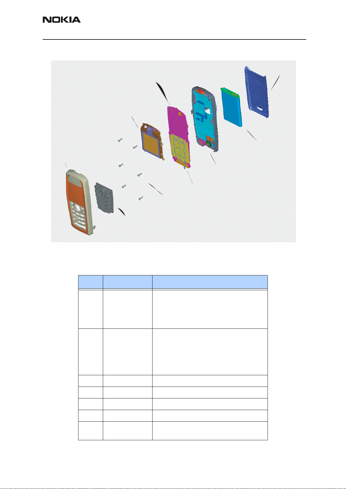
Exploded View
C-Cover
PWB
LCD Module
Assembly
A-Cover
Assembly
Screws (x6)
Keypad Assembly
Assembly Parts of Basic Transceiver RH-48
Qty Code Description
1
9491707
9491706
9491708
9491713
A-Cover Assembly
Graphite DMC06987
Light Grey DMC06987
Bright Blue DMC06987
Fun Fuchsia DMC06987
Battery
B-Cover (with Antenna
and Shield Assembly)
Dome Sheet Frame Assembly
1
9791124
9791427
9791132
9791130
9791125
6 6290119 Screws 1.8X6 RF T6+BLK DMD06930
1 9498012 LCD Module Assembly DMC06922
1 0202161 PWB
1 9481160 Dome Sheet Frame Assembly
1 9491626 B-Cover Assembly (with Antenna and Shield
Keypad Assembly
Latin DMC06505
Thai DMC07962
Hindi DMC06513
Stroke DMC06511
BOPOMOFO DMC06506
Assembly) DMC06814 Dark Grey
Issue 1 11/2003 Confidential ©2003 Nokia Corporation Page 3
Page 15
RH-48
Parts Lists CCS Technical Documentation
Qty Code Description
1 0670400 Battery (BL-5C)
1
9459321
9459316
9459317
9459460
1 9453375 C-Cover rel button DMD10535 Dark Grey
1 9510935 C-Cover rel spring DMD08481
1 9453340 B-Cover DMD11183 Blank
1 5140265 Mic Mod+Holder Tomahawk -42+-3DB
1 5400243 Conn DC-Jack 3.5mm 3POL SPR 90DEG
1 6800057 Vibra 1.3V 80MA
1 9453374 Power Button DMD10533 Dark Grey
1 9497263 D-Cover Assy DMC05545 HDDA2
1 0660303 Antenna Int. Ant. Assy
1 9517369 Shielding Assy DMC07076
1 9560199 SIM flap DMD08487
1 9481194 Conductive sticker
C-Cover
Graphite DMC07013
Light Grey DMC07013
Brt Blue DMC07013
Fuchsia DMC07013
1 9381480 RUIM sticker (Australia only)
Page 4 ©2003 Nokia Corporation Confidential Issue 1 11/2003
Page 16
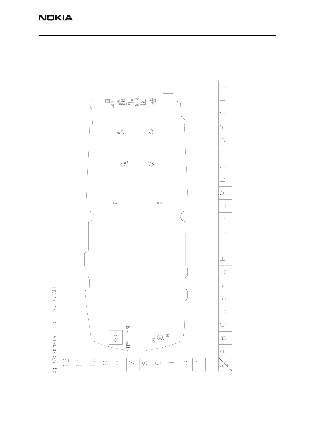
RH-48
CCS Technical Documentation Parts Lists
Component Layout — Top
Issue 1 11/2003 Confidential ©2003 Nokia Corporation Page 5
Page 17
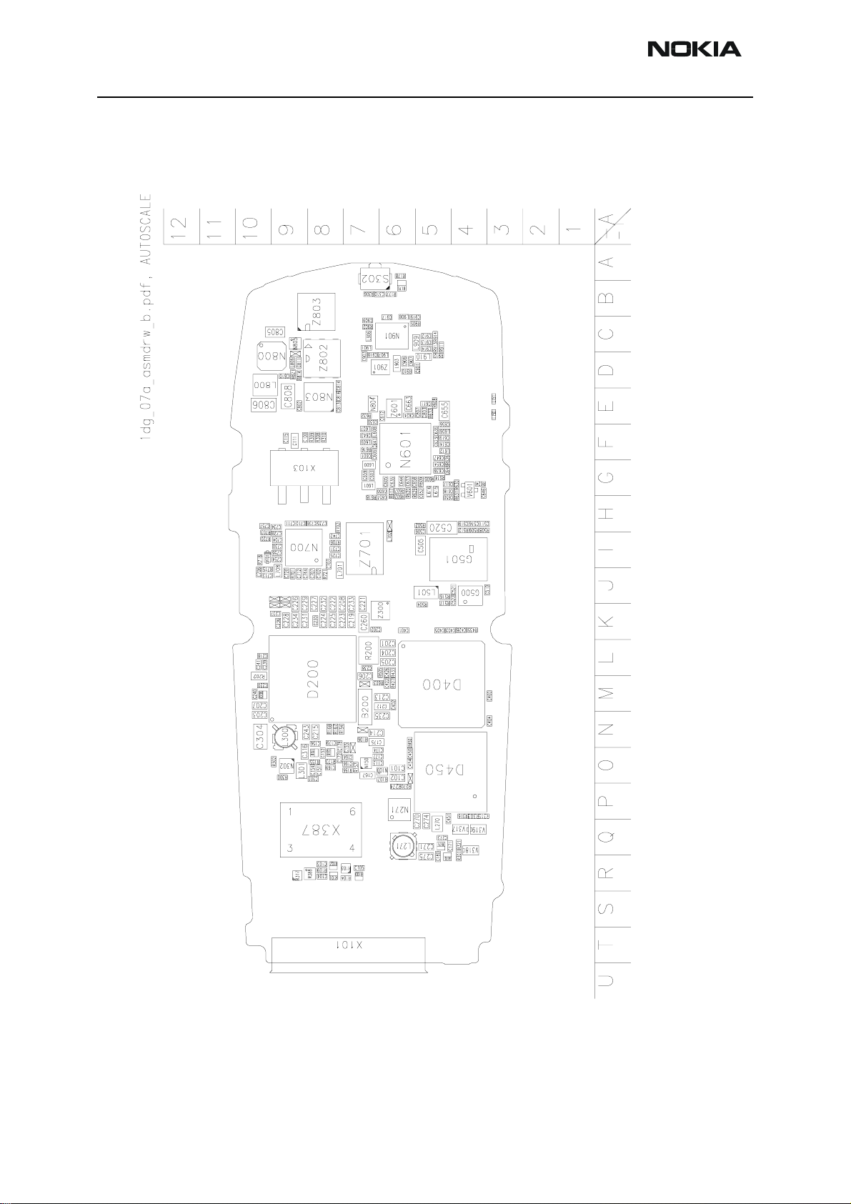
RH-48
Parts Lists CCS Technical Documentation
Component Layout — Bottom
Page 6 ©2003 Nokia Corporation Confidential Issue 1 11/2003
Page 18
RH-48
CCS Technical Documentation Parts Lists
Component Values — Top
Issue 1 11/2003 Confidential ©2003 Nokia Corporation Page 7
Page 19
RH-48
Parts Lists CCS Technical Documentation
Component Values — Bottom
Page 8 ©2003 Nokia Corporation Confidential Issue 1 11/2003
Page 20
RH-48
CCS Technical Documentation Parts Lists
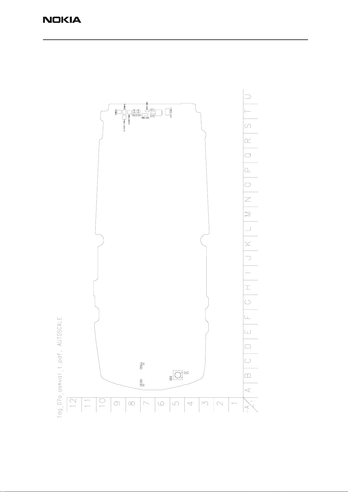
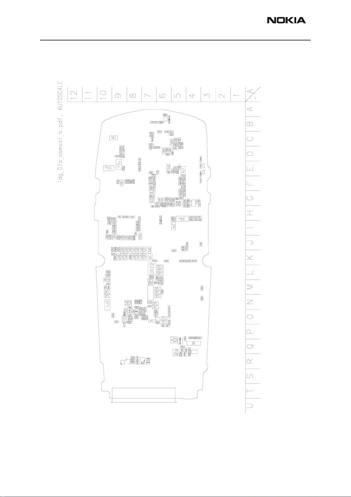
Parts List
RH-48 (3105) — EDMS Issue 10.0 Code: 0202161
Item Code Side X Y Description Value Type
R100 1620027 Bottom R 7 res network 0W06 2X47R J 0404
R101 1620027 Bottom R 8 res network 0W06 2X47R J 0404
R102 1620027 Bottom R 8 res network 0W06 2X47R J 0404
R103 4120011 Bottom R 7 ZDIX4 IP4043CX5 CA 14V2 10W CSP5
R104 1430812 Bottom R 7 chip res 0W06 220K J 0402
R105 1825031 Top T 9 varistor array 2XVWM16V VC50 0405
R106 1820039 Bottom Q 6 NTC res 0W1 47K J B=4050+-3% 0402
R107 1430804 Bottom Q 6 chip res 0W06 100K J 0402
R109 1430804 Bottom R 8 chip res 0W06 100K J 0402
R110 1825031 Top T 9 varistor array 2XVWM16V VC50 0405
R150 1620031 Top T 8 res network 0W06 2X1K0 J 0404
R151 1620031 Bottom O 8 res network 0W06 2X1K0 J 0404
R152 1620031 Top T 8 res network 0W06 2X1K0 J 0404
R154 1430744 Bottom N 8 chip res 0W06 470R J 0402
R155 1430796 Bottom O 8 chip res 0W06 47K J 0402
R156 1430191 Bottom O 7 chip res 0W06 180K 200PPM 0402
R157 1430772 Bottom O 7 chip res 0W06 5K6 J 0402
R167 1430693 Bottom N 8 chip res 0W06 5R6 J 0402
R168 1430693 Bottom N 8 chip res 0W06 5R6 J 0402
R170 1620031 Bottom Q 6 res network 0W06 2X1K0 J 0404
R171 1620031 Bottom Q 6 res network 0W06 2X1K0 J 0404
R172 1620031 Bottom O 8 res network 0W06 2X1K0 J 0404
R173 1430796 Bottom O 8 chip res 0W06 47K J 0402
R177 1430693 Bottom B 6 chip res 0W06 5R6 J 0402
R178 1430693 Bottom A 6 chip res 0W06 5R6 J 0402
R179 1825031 Bottom B 6 varistor array 2XVWM16V VC50 0405
R200 1419003 Bottom L 7 chip res 0W5 OR22 J 200PPM 1210
R202 1620067 Bottom M 10 res network 0W06 4X100K J 0804
R206 1620029 Bottom M 10 res network 0W06 2X4K7 J 0404
Issue 1 11/2003 Confidential ©2003 Nokia Corporation Page 9
Page 21

RH-48
Parts Lists CCS Technical Documentation
Item Code Side X Y Description Value Type
R270 1430690 Bottom Q 5 chip res jumper 0R0 0402
R271 1430690 Bottom Q 5 chip res jumper 0R0 0402
R275 1430690 Bottom Q 5 chip res jumper 0R0 0402
R277 1430690 Bottom Q 5 chip res jumper 0R0 0402
R300 1430915 Bottom O 9 chip res 0W06 1K3 F 250PPM 0402
R301 1430722 Bottom P 6 chip res 0W06 68R J 0402
R302 1430121 Bottom O 9 chip res 0W06 22K F 200PPM 0402
R303 1430722 Bottom O 6 chip res 0W06 68R J 0402
R306 1430770 Bottom B 7 chip res 0W06 4K7 J 0402
R308 1430722 Bottom F 8 chip res 0W06 68R J 0402
R309 1430734 Bottom F 8 chip res 0W06 220R J 0402
R310 1430734 Bottom F 8 chip res 0W06 220R J 0402
R315 1430714 Bottom O 6 chip res 0W06 33R J 0402
R316 1430722 Bottom P 6 chip res 0W06 68R J 0402
R317 4120011 Bottom R 9 ZDIX4 IP4043CX5 CA 14V2 10W CSP5
R321 1430764 Bottom P 6 chip res 0W06 3K3 j 0402
R388 4120071 Bottom R 8 ASIP EMIF03-SIM01 Sim Filter BGA8
R427 1430764 Bottom M 6 chip res 0W06 3K3 J 0402
R433 1430764 Bottom L 6 chip res 0W06 3K3 J 0402
R435 1430764 Bottom K 4 chip res 0W06 3K3 J 0402
R450 1430770 Bottom N 6 chip res 0W06 4K7 J 0402
R502 1430700 Bottom H 5 chip res 0W06 10R J 0402
R504 1430718 Bottom K 5 chip res 0W06 47R J 0402
R508 1430770 Bottom H 4 chip res 0W06 4K7 J 0402
R509 1430770 Bottom H 4 chip res 0W06 4K7 J 0402
R512 1430772 Bottom H 4 chip res 0W06 5K6 J 0402
R516 1430700 Bottom J 5 chip res 0W06 10R J 0402
R517 1430778 Bottom J 5 chip res 0W06 10K J 0402
R602 1430726 Bottom H 6 chip res 0W06 100R J 0402
R603 1430726 Bottom M 7 chip res 0W06 100R J 0402
R605 1430726 Bottom L 6 chip res 0W06 100R J 0402
R606 1430693 Bottom G 5 chip res 0W06 5R6 J 0402
Page 10 ©2003 Nokia Corporation Confidential Issue 1 11/2003
Page 22

RH-48
CCS Technical Documentation Parts Lists
Item Code Side X Y Description Value Type
R607 1430681 Bottom G 6 chip res 0W06 4R3 J 0402
R608 1430681 Bottom E 5 chip res 0W06 4R3 J 0402
R609 1430693 Bottom G 5 chip res 0W06 5R6 J 0402
R614 1430700 Bottom G 5 chip res 0W06 10R J 0402
R616 1430758 Bottom F 7 chip res 0W06 1K5 J 0402
R617 1430681 Bottom G 6 chip res 0W06 4R3 J 0402
R618 1430700 Bottom H 7 chip res 0W06 10R J 0402
R620 1430700 Bottom G 6 chip res 0W06 10R J 0402
R624 1430762 Bottom G 4 chip res 0W06 2K2 J 0402
R626 1430772 Bottom G 5 chip res 0W06 5K6 J 0402
R629 1430693 Bottom G 6 chip res 0W06 5R6 J 0402
R630 1430772 Bottom G 4 chip res 0W06 5K6 J 0402
R631 1430772 Bottom G 4 chip res 0W06 5K6 J 0402
R632 1430691 Bottom E 7 chip res 0W06 2R2 J 0402
R633 1430681 Bottom E 5 chip res 0W06 4R3 J 0402
R701 1430700 Bottom J 9 chip res 0W06 10R J 0402
R702 1430754 Bottom H 8 chip res 0W06 1K0 J 0402
R703 1430700 Bottom I 10 chip res 0W06 10R J 0402
R706 1430806 Bottom I 8 chip res 0W06 120K J 0402
R715 1430700 Bottom J 9 chip res 0W06 10R J 0402
R718 1430772 Bottom I 10 chip res 0W06 15K6 J 0402
R720 1430764 Bottom I 10 chip res 0W06 3K3 J 0402
R721 1430746 Bottom J 8 chip res 0W06 560R J 0402
R814 1430832 Bottom D 9 chip res 0W06 2K7 J 0402
R821 1820039 Bottom D 9 NTC res 0W1 47K J B=4050+-3% 0402
R902 1430796 Bottom C 7 chip res 0W06 47K J 0402
R905 1430724 Bottom C 5 chip res 0W06 82R J 0402
R910 1430693 Bottom D 6 chip res 0W06 5R6 J 0402
R911 1430708 Bottom C 5 chip res 0W06 18R J 0402
R912 1430738 Bottom D 5 chip res 0W06 270R J 0402
R913 1430738 Bottom C 5 chip res 0W06 270R J 0402
R914 1430690 Bottom C 5 chip res jumper 0R0 0402
Issue 1 11/2003 Confidential ©2003 Nokia Corporation Page 11
Page 23

RH-48
Parts Lists CCS Technical Documentation
Item Code Side X Y Description Value Type
C100 2320552 Bottom F 9 chip cap NP0 47P J 50V 0402
C101 2320481 Bottom Q 6 chip cap X5R 1U K 6V3 0603
C102 2320481 Bottom Q 6 chip cap X5R 1U K 6V3 0603
C103 2320544 Bottom R 8 chip cap NP0 22P J 50V 0402
C104 2320544 Bottom R 8 chip cap NP0 22P J 50V 0402
C105 2320544 Bottom R 7 chip cap NP0 22P J 50V 0402
C106 2320584 Top T 7 chip cap X7R 1N0 J 50V 0402
C111 2320110 Bottom F 9 chip cap X7R 10N K 50V 0603
C113 2320778 Bottom Q 6 chip cap X7R 10N K 16V 0402
C115 2320552 Bottom F 9 chip cap NP0 47P J 50V 0402
C151 2320805 Bottom O 8 chip cap X5R 100N K 10V 0402
C152 2320550 Bottom O 8 chip cap NP0 39P J 50V 0402
C153 2320552 Top T 8 chip cap NP0 47P J 50V 0402
C154 2320805 Bottom O 8 chip cap X5R 100N K 10V 0402
C155 2321007 Bottom O 7 cer cap X7R 22N K 16V 0402
C156 2320550 Bottom N 8 chip cap NP0 39P J 50V 0402
C164 2320592 Bottom O 7 chip cap X7R 2N2 J 50V 0402
C166 2321007 Bottom O 7 cer cap X7R 22N K 16V 0402
C167 2320481 Bottom O 7 chip cap X5R 1U K 6V3 0603
C169 2320805 Bottom O 8 chip cap X5R 100N K 10V 0402
C171 2320552 Bottom Q 6 chip cap NP0 47P J 50V 0402
C172 2320805 Bottom O 8 chip cap X5R 100N K 10V 0402
C174 2320805 Bottom O 7 chip cap X5R 100N K 10V 0402
C175 2320481 Bottom N 7 chip cap X5R 1U K 6V3 0603
C177 2320544 Bottom O 7 chip cap NP0 22P J 50V 0402
C178 2320550 Bottom N 8 chip cap NP0 39P J 50V 0402
C179 2320550 Bottom N 8 chip cap NP0 39P J 50V 0402
C180 2320805 Bottom R 6 chip cap X5R 100N K 10V 0402
C181 2320805 Top T 8 chip cap X5R 100N K 10V 0402
C201 2320481 Bottom L 6 chip cap X5R 1U K 6V3 0603
C202 2320778 Bottom K 7 chip cap X7R 10N K 16V 0402
C203 2320481 Bottom N 10 chip cap X5R 1U K 6V3 0603
Page 12 ©2003 Nokia Corporation Confidential Issue 1 11/2003
Page 24

RH-48
CCS Technical Documentation Parts Lists
Item Code Side X Y Description Value Type
C204 2320481 Bottom L 6 chip cap X5R 1U K 6V3 0603
C205 2320481 Bottom L 6 chip cap X5R 1U K 6V3 0603
C206 2320481 Bottom M 7 chip cap X5R 1U K 6V3 0603
C207 2320481 Bottom M 10 chip cap X5R 1U K 6V3 0603
C208 2320481 Bottom K 8 chip cap X5R 1U K 6V3 0603
C212 2320481 Bottom M 6 chip cap X5R 1U K 6V3 0603
C213 2320481 Bottom M 6 chip cap X5R 1U K 6V3 0603
C214 2320481 Bottom N 7 chip cap X5R 1U K 6V3 0603
C215 2320481 Bottom N 8 chip cap X5R 1U K 6V3 0603
C218 2320805 Bottom L 10 chip cap X5R 100N K 10V 0402
C219 2320481 Bottom K 7 chip cap X5R 1U K 6V3 0603
C220 2320778 Bottom M 10 chip cap X7R 10N K 16V 0402
C221 2320481 Bottom K 7 chip cap X5R 1U K 6V3 0603
C222 2320481 Bottom K 8 chip cap X5R 1U K 6V3 0603
C223 2320481 Bottom K 8 chip cap X5R 1U K 6V3 0603
C224 2320481 Bottom K 8 chip cap X5R 1U K 6V3 0603
C225 2320481 Bottom K 8 chip cap X5R 1U K 6V3 0603
C226 2320481 Bottom K 9 chip cap X5R 1U K 6V3 0603
C227 2320481 Bottom K 8 chip cap X5R 1U K 6V3 0603
C228 2320481 Bottom K 9 chip cap X5R 1U K 6V3 0603
C229 2320481 Bottom K 9 chip cap X5R 1U K 6V3 0603
C230 2320805 Bottom K 8 chip cap X5R 100N K 10V 0402
C231 2320481 Bottom K 9 chip cap X5R 1U K 6V3 0603
C232 2320481 Bottom K 8 chip cap X5R 1U K 6V3 0603
C233 2320481 Bottom K 7 chip cap X5R 1U K 6V3 0603
C234 2320481 Bottom K 9 chip cap X5R 1U K 6V3 0603
C235 2320481 Bottom N 6 chip cap X5R 1U K 6V3 0603
C236 2320805 Bottom K 9 chip cap X5R 100N K 10V 0402
C237 2320805 Bottom K 9 chip cap X5R 100N K 10V 0402
C238 2320143 Bottom L 7 chip cap X5R 220N K 6.3V 0402
C239 2320805 Bottom L 10 chip cap X5R 100N K 10V 0402
C240 2320778 Bottom M 10 chip cap X7R 10N K 16V 0402
Issue 1 11/2003 Confidential ©2003 Nokia Corporation Page 13
Page 25
RH-48
Parts Lists CCS Technical Documentation
Item Code Side X Y Description Value Type
C241 2320778 Bottom L 10 chip cap X7R 10N K 16V 0402
C243 2320481 Bottom N 9 chip cap X5R 1U K 6V3 0603
C260 2310037 Bottom K 7 chip cap X5R 10U M 6V3 0805
C270 2320505 Bottom Q 5 chip cap X5R 4U7 K 6.3V 0603
C271 2320505 Bottom Q 4 chip cap X5R 4U7 K 6.3V 0603
C273 2320805 Bottom Q 5 chip cap X5R 100N K 10V 0402
C274 2320505 Bottom Q 5 chip cap X5R 4U7 K 6.3V 0603
C275 2320505 Bottom R 4 chip cap X5R 4U7 K 6.3V 0603
C300 2320805 Top B 7 chip cap X5R 100N K 10V 0402
C301 2320805 Top C 7 chip cap X5R 100N K 10V 0402
C303 2320805 Bottom O 8 chip cap X5R 100N K 10V 0402
C304 2312411 Bottom N 10 chip cap X5R 1U0 M 25V 1206
C306 2320552 Top A 7 chip cap NP0 47P J 50V 0402
C309 2320552 Top C 7 chip cap NP0 47P J 50V 0402
C310 2320778 Bottom B 6 chip cap X7R 10N K 16V 0402
C316 2320481 Bottom O 9 chip cap X5R 1U K 6V3 0603
C400 2320805 Bottom M 3 chip cap X5R 100N K 10V 0402
C401 2320805 Bottom K 6 chip cap X5R 100N K 10V 0402
C402 2320805 Bottom M 6 chip cap X5R 100N K 10V 0402
C403 2320805 Bottom K 5 chip cap X5R 100N K 10V 0402
C404 2320805 Bottom N 3 chip cap X5R 100N K 10V 0402
C405 2320805 Bottom K 5 chip cap X5R 100N K 10V 0402
C422 2320778 Bottom M 6 chip cap X7R 10N K 16V 0402
C426 2320778 Bottom L 6 chip cap X7R 10N K 16V 0402
C428 2320778 Bottom K 4 chip cap X7R 10N K 16V 0402
C450 2320778 Bottom O 6 chip cap X7R 10N K 16V 0402
C451 2320805 Bottom P 5 chip cap X5R 100N K 10V 0402
C454 2320778 Bottom O 6 chip cap X7R 10N K 16V 0402
C505 2312243 Bottom I 5 chip cap X5R 4U7 K 6V3 0805
C506 2320548 Bottom I 5 chip cap NP0 33P J 50V 0402
C510 2320584 Bottom J 3 chip cap X7R 1N0 J 50V 0402
C511 2320584 Bottom H 4 chip cap X7R 1N0 J 50V 0402
Page 14 ©2003 Nokia Corporation Confidential Issue 1 11/2003
Page 26

RH-48
CCS Technical Documentation Parts Lists
Item Code Side X Y Description Value Type
C516 2320588 Bottom H 4 chip cap X7R 1N5 J 50V 0402
C519 2320618 Bottom H 4 chip cap X7R 4N7 J 25V 0402
C520 2420029 Bottom H 5 chip cap PPS 39N G 16V 1206
C521 2320805 Bottom J 4 chip cap X5R 100N K 10V 0402
C522 2320584 Bottom J 4 chip cap X7R 1N0 J 50V 0402
C600 2320584 Bottom G 6 chip cap X7R 1N0 J 50V 0402
C601 2320596 Bottom F 7 chip cap X7R 3N3 J 50V 0402
C603 2320540 Bottom G 7 chip cap NP0 15P J 50V 0402
C605 2320584 Bottom G 6 chip cap X7R 1N0 J 50V 0402
C606 2320584 Bottom F 7 chip cap X7R 1N0 J 50V 0402
C611 2320584 Bottom E 5 chip cap X7R 1N0 J 50V 0402
C612 2320584 Bottom E 6 chip cap X7R 1N0 J 50V 0402
C614 2320520 Bottom F 5 chip cap NP0 2P2 C 50V 0402
C617 2320538 Bottom G 5 chip cap NP0 12P J50V 0402
C618 2320538 Bottom G 5 chip cap NP0 12P J50V 0402
C619 2320516 Bottom F 5 chip cap NP0 1P5 C 50V 0402
C623 2320520 Bottom F 5 chip cap NP0 2P2 C 50V 0402
C624 2320550 Bottom F 5 chip cap NP0 39P J 50V 0402
C630 2320544 Bottom E 7 chip cap NP0 22P J 50V 0402
C633 2320584 Bottom G 6 chip cap X7R 1N0 J 50V 0402
C635 2320584 Bottom G 6 chip cap X7R 1N0 J 50V 0402
C636 2320805 Bottom G 5 chip cap X5R 100N K 10V 0402
C638 2320584 Bottom G 5 chip cap X7R 1N0 J 50V 0402
C641 2320621 Bottom F 7 chip cap NP0 0P5 C 50V 0402
C643 2320584 Bottom F 7 chip cap X7R 1N0 J 50V 0402
C644 2320560 Bottom G 6 chip cap NP0 100P J 50V 0402
C646 2320592 Bottom G 4 chip cap X7R 2N2 J 50V 0402
C647 2320592 Bottom F 5 chip cap X7R 2N2 J 50V 0402
C648 2320771 Bottom G 5 chip cap X5R 27N K 10V 0402
C650 2320778 Bottom H 5 chip cap X7R 10N K 16V 0402
C651 2320805 Bottom H 6 chip cap X5R 100N K 10V 0402
C652 2320778 Bottom G 5 chip cap X7R 10N K 16V 0402
Issue 1 11/2003 Confidential ©2003 Nokia Corporation Page 15
Page 27

RH-48
Parts Lists CCS Technical Documentation
Item Code Side X Y Description Value Type
C654 2320805 Bottom G 5 chip cap X5R 100N K 10V 0402
C655 2312243 Bottom E 5 chip cap X5R 4U7 K 6V3 0805
C656 2320552 Bottom F 5 chip cap NP0 47P J 50V 0402
C658 2320584 Bottom G 6 chip cap X7R 1N0 J 50V 0402
C659 2320560 Bottom G 7 chip cap NP0 100P J 50V 0402
C663 2320481 Bottom E 6 chip cap X5R 1U K 6V3 0603
C702 2320552 Bottom J 8 chip cap NP0 47P J 50V 0402
C703 2320778 Bottom I 8 chip cap X7R 10N K 16V 0402
C704 2320778 Bottom I 9 chip cap X7R 10N K 16V 0402
C706 2320584 Bottom J 10 chip cap X7R 1N0 J 50V 0402
C707 2320552 Bottom J 8 chip cap NP0 47P J 50V 0402
C710 2320805 Bottom H 9 chip cap X5R 100N K 10V 0402
C711 2320538 Bottom H 9 chip cap NP0 12P J50V 0402
C712 2320584 Bottom J 9 chip cap X7R 1N0 J 50V 0402
C713 2320620 Bottom J 10 chip cap X7R 10N J 16V 0402
C720 2320805 Bottom J 9 chip cap X5R 100N K 10V 0402
C725 2320805 Bottom I 8 chip cap X5R 100N K 10V 0402
C728 2320760 Bottom I 9 chip cap X7R 4N7 K 25V 0402
C730 2320805 Bottom I 9 chip cap X5R 100N K 10V 0402
C731 2320805 Bottom I 8 chip cap X5R 100N K 10V 0402
C734 2320805 Bottom H 9 chip cap X5R 100N K 10V 0402
C735 2320584 Bottom H 8 chip cap X7R 1N0 J 50V 0402
C736 2320584 Bottom H 8 chip cap X7R 1N0 J 50V 0402
C742 2320805 Bottom I 8 chip cap X5R 100N K 10V 0402
C744 2320620 Bottom J 9 chip cap X7R 10N J 16V 0402
C754 2320009 Bottom I 9 chip cap NP0 10P J 50V 0402
C756 2320787 Bottom I 9 chip cap X7R 15N K 16V 0402
C757 2320805 Bottom H 10 chip cap X5R 100N K 10V 0402
C802 2320564 Bottom E 9 chip cap NP0 150P J 50V 0402
C803 2320805 Bottom E 5 chip cap X5R 100N K 10V 0402
C805 2310037 Bottom C 9 chip cap X5R 10U M 6V3 0805
C806 2312255 Bottom E 10 chip cap X5R 10U K 10V 1206
Page 16 ©2003 Nokia Corporation Confidential Issue 1 11/2003
Page 28
RH-48
CCS Technical Documentation Parts Lists
Item Code Side X Y Description Value Type
C807 2320783 Bottom E 5 chip cap X7R 33N K 10V 0402
C808 2312255 Bottom E 9 chip cap X5R 10U K 10V 1206
C810 2320778 Bottom D 9 chip cap X7R 10N K 16V 0402
C811 2320508 Bottom D 9 chip cap NP0 1P0 C 50V 0402
C813 2320576 Bottom E 8 chip cap X7R 470P J 50V 0402
C814 2320584 Bottom D 8 chip cap X7R 1N0 J 50V 0402
C816 2320778 Bottom E 8 chip cap X7R 10N K 16V 0402
C901 2320554 Bottom D 5 chip cap NP0 56P J 50V 0402
C903 2320518 Bottom D 7 chip cap NP0 1P8 C 50V 0402
C906 2320560 Bottom D 6 chip cap NP0 100P J 50V 0402
C907 2320524 Bottom D 6 chip cap NP0 3P3 C 50V 0402
C909 2320560 Bottom C 7 chip cap NP0 100P J 50V 0402
C912 2320526 Bottom C 5 chip cap NP0 3P9 C 50V 0402
C913 2320596 Bottom C 5 chip cap X7R 3N3 J 50V 0402
C914 2320805 Bottom C 5 chip cap X5R 100N K 10V 0402
C917 2320546 Bottom C 6 chip cap NP0 27P J 50V 0402
C918 2320785 Bottom D 7 chip cap X7R 47N K 10V 0402
C919 2320584 Bottom C 5 chip cap X7R 1N0 J 50V 0402
L100 3203705 Top T 6 ferrite bead 0.015R 42R/100M 0805
L102 3203801 Top T 8 chip bead array 2X1000R 0405
L103 3203801 Top T 9 chip bead array 2X1000R 0405
L106 3203725 Top T 7 ferrite bead 600R/100MHz 0402
L107 3203741 Top T 7 ferrite bead 0R5 0R5 600R/100MHz 0603
L150 3203767 Bottom E 3 ferrite bead 240R/100M 0.4A 0R3 0402
L151 3203767 Bottom E 3 ferrite bead 240R/100M 0.4A 0R3 0402
L270 3203743 Bottom Q 5 ferrite bead 0R03 42R/100MHz 3A 0805
L271 Bottom Q 4 choke coil DC/DC 10UH 3.6X3.6X1.2
L300 3640119 Bottom N 9 choke 22U M 1R4 0.33A 3.3X3.3X1.5
L301 3203743 Bottom O 9 ferrite bead 0R03 42R/100MHz 3A 0805
L501 4550257 Bottom J 5 Dir Coupler 1066+-14MHz 3.2X1.6
L600 3645305 Bottom G 7 chip coil 12N G Q35/250MHz 0603
L601 3645305 Bottom G 7 chip coil 12N G Q35/250MHz 0603
Issue 1 11/2003 Confidential ©2003 Nokia Corporation Page 17
Page 29

RH-48
Parts Lists CCS Technical Documentation
Item Code Side X Y Description Value Type
L606 3646001 Bottom F 5 chip coil 3N3 +-0N3 Q7/100M 0402
L607 3646039 Bottom F 7 chip coil 5N6 +-0N3 Q7/100M 0402
L608 3646039 Bottom F 7 chip coil 5N6 +-0N3 Q7/100M 0402
L609 3646039 Bottom F 7 chip coil 5N6 +-0N3 Q7/100M 0402
L612 3646099 Bottom F 5 chip coil 2N7 +-0N3 Q29/800M 0402
L615 3646017 Bottom G 5 chip coil 12N J Q7/100MHz 0402
L616 3646017 Bottom G 5 chip coil 12N J Q7/100MHz 0402
L701 3645243 Bottom J 8 chip coil 47N J Q38/200MHz 0603
L702 3646027 Bottom I 6 chip coil 33N J Q7/100MHz 0402
L708 3645213 Bottom J 9 chip coil 22N J Q38/250MHz 0603
L800 3640133 Bottom D 10 chip coil 2U7 K Q21/1MHz 3.0X3.4
L802 Top B 5 chip coil 68N J Q8/100MHz 0402
L806 3646027 Bottom D 9 chip coil 33N J Q7/100MHz 0402
L901 3646017 Bottom C 7 chip coil 12N J Q7/100MHz 0402
L903 3645189 Bottom D 6 chip coil 100N J Q12/100MHz 0603
L906 3646415 Bottom C 7 chip coil 19N J Q24/250MHz 0402
L907 3646019 Bottom D 6 chip coil 15N J Q7/100MHz 0402
L908 3646237 Bottom C 6 chip coil 18N J Q7/100MHz 0402
L909 3645161 Bottom C 5 chip coil 150N J Q14/100MHz 0603
L910 3645011 Bottom D 5 chip coil 68NH J Q12/100MHz 3.0X3.4
V100 4113721 Top T 6 TVS Di 1PMT16AT3 16V 175W PWRMITE
V307 4860339 Top O 6 LED LWL88S
V308 4860339 Top O 8 LED LWL88S
V309 4860339 Top R 6 LED LWL88S
V312 4860339 Top R 8 LED LWL88S
V313 4860339 Top L 5 LED LWL88S
V314 4860339 Top L 8 LED LWL88S
V317 4219937 Bottom P 6 TRX2 UMT1/PUMT1 P40V100MA SOT363
V318 4219937 Bottom P 6 TRX2 UMT1/PUMT1 P40V100MA SOT363
V319 4219937 Bottom O 6 TRX2 UMT1/PUMT1 P40V100MA SOT363
V601 4110945 Bottom G 4 Cap DIX2 BBY57-05W 4P7/17P SOT323
V701 4110921 Bottom I 10 Cap DI BBY57-02W 1/4 16/4P SOD523
Page 18 ©2003 Nokia Corporation Confidential Issue 1 11/2003
Page 30

RH-48
CCS Technical Documentation Parts Lists
Item Code Side X Y Description Value Type
Z300 4120031 Bottom K 6 EMI/ESD Filt EMIF10- 1K010F1 BGA24
Z601 4511365 Bottom E 6 Saw Filt 836.5+-12.5M/ 3DB 2.5X2
Z701 4511387 Bottom I 7 Saw Filt 183.6+-0.63Mhz 7X5X1.3
Z802 4510329 Bottom D 8 Isolator 824-849MHz .65DB 5X5X2
Z803 4512179 Bottom B 8 Dupl 824-849/ 869-894MHz 5X5X1.8
Z901 4511379 Bottom D 6 Saw Filt 881.5+-12.5M/ 2.5 2X2.5
N100 4341421 Bottom Q 6 VREG 2.8V/150MA (LP3985) USMD5
N150 4341429 Bottom O 7 AF AMP 0.4W/2.6V (LM4890ITLX) USMD9
N271 4341609 Bottom P 6
N302 Bottom O 9 DC/DC Conv LM3500 / TK65600 USMD8
N601 4370941 Bottom F 6 Jedi TX RFIC
N700 4370937 Bottom I 9 Yoda DIG-V1 Metal Mod I.F IC 5X5
N800 4341487 Bottom D 9 Vreg Elec-Adj (CX20504) MLF16
N803 4350405 Bottom E 8 PW Amp CX77145 CDMA800 ORCA
N804 4219935 Bottom E 7 TRX2+4X10K PUMD3 N&P 50V SOT363
N805 4120091 Bottom C 9 ASIP STPAC01-F1 CDMA Pwr Det BGA8
N901 4370863 Bottom C 6 Alfred LNA/Mixer/ VQFN-24
G500 4510435 Bottom J 4 VCTCXO 19.2MHz 2.78V 2.2MA
G501 4350429 Bottom I 4 VCO 1051 - 1082MHz
2.78V 10MA
D200 4370825 Bottom M 8 UEMK W-DOG ENA TO21 TFBGA168
D400 4375017 Bottom M 5 UPP8M V3.01B2 F751542A UBGA144
D450 4341501 Bottom O 5 Combo 128M NOR + 8M SRAM TBGA48
B200 4510303 Bottom M 7 Crystal 32.768kHZ +-20PPM 12.5PF
F100 5119019 Top T 5 Sm Fuse F 1.5A 32V 0603
S302 5200025 Bottom A 7 Sm Tact SW Side Travel 0.2MM
CDMA
X101 5460061 Bottom T 7 Sm System Connector 14POL
X103 5409253 Bottom G 9 Sm Battery Conn 3POL Spr 12V 2A
X302 5469175 Top B 8 Sm Conn 2X5F P0.5 PWB/PWB
X387 5409219 Bottom Q 8 Sm SIM Connector 6POL P2.54
X801 5420047 Top B 5 Sm Coax Conn + SW F 50R 250V 6GHz
Issue 1 11/2003 Confidential ©2003 Nokia Corporation Page 19
Page 31

RH-48
Parts Lists CCS Technical Documentation
Page 20 ©2003 Nokia Corporation Confidential Issue 1 11/2003
Page 32

CCS Technical Documentation
RH-48 Series Transceivers
Service Software Instructions
Issue 1 11/2003 Confidential ©2003 Nokia Corporation
Page 33

RH-48
Service Software Instructions CCS Technical Documentation
Contents
Page No
Phoenix User’s Guide .................................................................................................... 3
Introduction ..................................................................................................................3
General Setup Procedure........................................................................................... 3
Hardware Requirements for using Phoenix .............................................................. 4
Installing Phoenix ........................................................................................................4
Installation Directions............................................................................................... 4
Software Support Bundles ...........................................................................................4
Starting a Phoenix Session ...........................................................................................5
Concepts.................................................................................................................... 5
Initial Session with Phoenix...................................................................................... 5
Scanning for a Product.............................................................................................. 6
Using Components.................................................................................................... 7
Using Profiles............................................................................................................ 7
Uninstalling Phoenix ...................................................................................................7
Uninstalling Phoenix version.................................................................................... 7
Diego User’s Guide........................................................................................................ 8
Introduction ..................................................................................................................8
General Setup Procedure........................................................................................... 8
Hardware Requirements for using Diego.................................................................. 9
Installing Diego ...........................................................................................................9
Installing.................................................................................................................... 9
Software Support Bundles .........................................................................................10
Starting a Diego Session ............................................................................................10
Concepts.................................................................................................................. 10
Initial Session with Diego and FLS-4S Dongle...................................................... 10
Scanning for a Product............................................................................................ 12
Using Components.................................................................................................. 12
Uninstalling Diego .....................................................................................................12
Uninstalling Diego version...................................................................................... 13
Page 2 ©2003 Nokia Corporation Confidential Issue 1 11/2003
Page 34

RH-48
CCS Technical Documentation Service Software Instructions
Phoenix User’s Guide
Introduction
This section briefly describes how to install Phoenix and includes some basic information
on how to use the program. More detailed information can be found in the Phoenix Help
files. Each feature in Phoenix has its own Help file, which can be activated whil running
Phoenix. To activate a Help file while Phoenix is running, press the F1 key or the specific
feature’s Help button.
General Setup Procedure
Initial installation of Phoenix requires the complete Phoenix installation package. This
package, currently around 30 Megabytes in size, is provided on a CD-ROM disk. Because
of this large size, it is not recommended to download the file nor is it practical to provide
it on 3.5-inch floppy disks.
Install Phoenix by following the steps outlined on the material that comes with the disk.
It should be noted that installation of a Nokia dongle on the computer being loaded is
REQUIRED prior to beginning the installation of the software.
The software is packaged into an Installshield executable bundle. When the user doubleclicks on this file, the installation program provides on-screen instructions on how to
proceed. Standard installation, provided by selecting all default choices, is highly recommended. You may do a custom installation and place Phoenix into a special location on
your hard drive, but this is only recommended for experienced users.
It is necessary to reboot the computer after installing the software. The program will not
be usable until a reboot is performed. After reboot, the Phoenix icon is displayed on the
computer desktop. Double-clicking on this icon launches the program.
Issue 1 11/2003 Confidential ©2003 Nokia Corporation Page 3
Page 35

RH-48
Service Software Instructions CCS Technical Documentation
Hardware Requirements for using Phoenix
Minimum Hardware Requirements
Processor 233 MHz
RAM1 64 MB
Disk space needed 50-100 MB
Supported Operating
Windows 95 Limited, no USB support
Windows 98
Windows NT 4.0 no USB support
Windows 2000 Professional version
Installing Phoenix
Before installing the software, verify:
• The dongle is attached to the parallel port for PKD version dongles, or an FLS-4 version
dongle is attached on either the parallel port or the USB port (if the computer supports
USB).
• Ensure that if the computer supports administrator rights (typically on Windows NT
and Windows 2000 installations) that access is enabled for the user performing the
Phoenix installation.
• If a previous version of Phoenix has been installed, it may be necessary to first properly
remove that program prior to installing the new version. If installation is performed,
be sure to reboot the computer prior to continuing. See the section Uninstalling
Phoenix for instructions on how to uninstall.
Systems
Notes
Installation Directions
• Insert the CD-ROM disk into the computer drive
• Access the drive and double-click on the Phoenix software package found on the CD.
• Follow the on-screen prompts to conclusion.
Note that rebooting the computer may be necessary when completed.
Software Support Bundles
The Phoenix installation is auto-executable. You must obtain Software Support Bundles
Page 4 ©2003 Nokia Corporation Confidential Issue 1 11/2003
Page 36

RH-48
CCS Technical Documentation Service Software Instructions
to load software upgrade files to customer-specific phone models.
These bundles are created by CCS and made available by AMS on the Partners Web Page
http://americas.partners.nokia.com. This web page is password-controlled; if you have
not registered as a user, contact Nokia Central Service in Melbourne, Florida.
Similar to the Phoenix installation, these Software Support Bundles are InstallShield executable packages. Just double-click on the package and it will auto-install.
No rebooting of the computer is required.
Starting a Phoenix Session
Concepts
When referring to Phoenix, Product is the cellular phone attached to the computer.
More specifically, it is the particular type of phone.
Connection is the type of cable used to attach the phone and the port on the computer
where it is attached. Refer to the Service Tools chapter for additional information.
The first time Phoenix is used, certain connection configurations must be made. Subsequent uses will rely on these selections and they will not need to be made again.
Initial Session with Phoenix
It is necessary to create the connection the first time Phoenix is used. Follow these simple steps:
Select Manage Connections… from the “File” drop-down menu.
Issue 1 11/2003 Confidential ©2003 Nokia Corporation Page 5
Page 37

RH-48
Service Software Instructions CCS Technical Documentation
Next click the Add… button to create a new connection.
When the Select Mode dialog box appears, you may then select either Wizard, which will
auto-detect your connection configuration, or Manual, which allows you to manually
select options to create the connection.
Once a connection is defined, make sure that the one to be used is moved to the top of
the list (use the up down arrows on the Manage Connections dialog box. Then click on
the Apply button. Close the window when finished.
You can now proceed with the normal initiation of a session by selecting a product or
scanning for a product.
Scanning for a Product
Many features of this program are product-specific. Therefore it is necessary to configure Phoenix for the product on which you will be working at the beginning of the session.
Scan Product – Choose Scan Product from the drop-down menu list and Phoenix will
automatically scan for product and select the necessary configurations. The status bar
Page 6 ©2003 Nokia Corporation Confidential Issue 1 11/2003
Page 38

RH-48
CCS Technical Documentation Service Software Instructions
at the bottom will indicate if the product was found and its type.
Using Components
When working with Phoenix, tasks are generally managed by specific software components. From the menu, select the desired component or task to be performed.
“Opening a component” is defined as opening a tool window within Phoenix. When this
window is opened, Phoenix also opens a toolbar for it and adds component-specific
menu items in the Window menu.
Using Profiles
Phoenix’s Profile feature allows product, connection and currently open components to
be stored into permanent storage by creating a profile file with a name of your choice
followed by an .nmp file extension for later retrieval.
Saved profiles makes it easy to configure Phoenix into a desired configuration with
favorite windows already opened and ready to go.
Opening and saving profiles is done via menu commands found in the File drop-down
menu: Open Profile and Save Profile.
Profiles are stored into a disk file with user-defined names. As a result, there can be
multiple profiles for different repeated tasks or user preferences.
Uninstalling Phoenix
As mentioned in the Installing Phoenix section, it may be necessary or desirable to
remove Phoenix. Care must be taken to follow this procedure. Failure to remove the
program properly will cause misconfiguration of the computer’s registry.
Uninstalling Phoenix version
• Access the computer’s “Control Panel” section, selectable from the Start button or the
“My Computer” desktop icon
• Select the “Add/Remove Programs” icon
• Select the Phoenix version to be removed, and click the Add/Remove button
• Click on the OK button to begin the process of removal
• Follow the on-screen instructions
Be sure to reboot the computer when finished.
Issue 1 11/2003 Confidential ©2003 Nokia Corporation Page 7
Page 39

RH-48
Service Software Instructions CCS Technical Documentation
Diego User’s Guide
Introduction
This section briefly describes how to install Diego and includes some basic information
on how to use the program. More detailed information can be found in the Diego Help
files. Each feature in Diego has its own Help file, which can be activated while running
Diego. To activate a Help file while Diego is running, press the F1 key or the specific feature’s Help button.
Diego is designed to be used by point of sales locations. Ease of use and minimal operator decision-making were key factors in the design. Additionally, this Diego version is
compatible with current-generation phones (DCT3 versions such as 5185i, 5170i, 5180i,
6185i, and 3285) and DCT4 versions such as the 6385.
General Setup Procedure
Initial installation of Diego requires the complete Diego installation package. This package, currently around 18 megabytes in size, is provided on a CD-ROM disk. Because of
this large size, it is not recommended to download the file nor is it practical to provide it
on 3.5-inch floppy disks.
Install Diego by following the steps as outlined on the material that comes with the disk.
It should be noted that installation of a Nokia dongle on the computer being loaded is
REQUIRED prior to beginning the installation of the software.
The software is packaged into an InstallShield executable bundle. When the user double-clicks on this file, the installation program provides on-screen instructions on how to
proceed. Standard installation, provided by selecting all default choices, is highly recommended. You may do a custom installation and place Diego into a special location on
your hard drive; however, this is only recommended for experienced users.
It is necessary to reboot the computer after installing the software. The program is not
usable until a reboot is performed. After reboot, the Diego icon is included on the computer desktop. Double-clicking on this icon launches the program.
Page 8 ©2003 Nokia Corporation Confidential Issue 1 11/2003
Page 40

RH-48
CCS Technical Documentation Service Software Instructions
Hardware Requirements for using Diego
Minimum Hardware Requirements
Processor 233 MHz
RAM1 64 MB
Disk space needed 50-100 MB
Windows 95 Limited, no USB support
Windows 98
Windows NT 4.0 no USB support
Windows 2000 Professional version
Installing Diego
Before installing the software, verify:
• An FLS-4 version dongle is attached to either the parallel port or the USB port (if the
computer supports USB). An FLS-2D may be used; however, the FLS-2D does not support the new generation DCT-4 version phones.
• Ensure that if the computer supports administrator rights (typically on Windows NT
and Windows 2000 installations) that access is enabled for the user performing the
installation.
• If a previous version of Diego has been installed, it may be necessary to first properly
remove that program prior to installing the new version. If installation is performed,
be sure to reboot the computer prior to continuing. See Uninstalling Diego for
instructions on how to uninstall.
Supported Operating
Systems
Notes
Installing
• Insert the CD-ROM disk into the computer drive.
• Access the drive and double-click on the Diego software package found on the CD.
• Follow the on-screen prompts to conclusion.
Issue 1 11/2003 Confidential ©2003 Nokia Corporation Page 9
Page 41

RH-48
Service Software Instructions CCS Technical Documentation
Note that rebooting the computer will be necessary when completed.
Software Support Bundles
The Diego installation is auto-executable. You must obtain Software Support Bundles to
load software upgrade files to customer-specific models.
These bundles are created by CCS and made available by AMS on the Partners Web Page
http://americas.partners.nokia.com . This web page is password-controlled; if you have
not registered as a user, contact Nokia Central Service in Melbourne, Florida.
Similar to the Diego installation, these packages are executable packages. Just doubleclick on the package, and it will auto-install.
No re-booting of the computer is required.
Starting a Diego Session
Concepts
When referring to Diego, Product is the cellular phone attached to the computer. More
specifically, it is the particular type of phone.
Connection is the type of cable used to attach the phone and the port on the computer
where it is attached. Refer to the Service Tools chapter for more information.
The first time Diego is used, certain connection configurations must be made. Subsequent uses will rely on these selections and they will not need to be made again.
Initial Session with Diego and FLS-4S Dongle
You must configure the Virtual Port Connection in Diego the first time Diego is launched.
The FLS-4 dongle uses virtual port, which eliminates the need to use the serial port (as
the FLS-2D does). During the installation of the FLS-4 drivers (included in the Diego
installation package), a virtual COM port is set to the next available COM port number.
This port selection must be put into the Diego configuration.
Follow these simple steps:
Page 10 ©2003 Nokia Corporation Confidential Issue 1 11/2003
Page 42

RH-48
N
CCS Technical Documentation Service Software Instructions
Select “My Computer” desktop icon and click on the “FLS Virtual Port” icon.
Make note of the Virtual Port Assignment (COM 2 in this example).
Next select “Add…” to create a new connection.
ote: COM port settings can
only be entered or changed if
the auto-connection feature of
Diego is disable (as indicated
by the grey Status box).
To disable the auto-connect
click on this icon in the tool
bar:
Note: COM port settings can only be entered or changed if the auto-connection feature of Diego is
disabled (as indicated in the grey Status box). To disable the auto-connect feature, click on this icon in
the toolbar.
Issue 1 11/2003 Confidential ©2003 Nokia Corporation Page 11
Page 43

RH-48
Service Software Instructions CCS Technical Documentation
Select the Virtual COM port setting. Then press the Apply button.
You can now proceed with the normal initiation of a session.
Scanning for a Product
Many features of this program are product-specific. Therefore, it is necessary to configure Diego at the beginning of a session for the product on which you will be working.
Scanning of the product can be done manually or automatically. The default setting is
automatic. This setting can be changed to manual in the “settings” – “general” box. In
automatic mode, Diego will automatically scan for a product at a periodic rate. The scan
rate is defaulted to every 5 seconds, but it can be changed to a different frequency in the
Setup menu.
To manually scan for a product, click on the “Settings” icon as noted above.
Using Components
When working with Diego, tasks are generally managed by specific software components. From the icons displayed on the left side of the screen, select the desired component or task to be performed.
“Opening a component” is defined as opening a tool window within Diego. When this
window is opened, Diego also opens a task box for it, which includes component-specific menu items.
Uninstalling Diego
As mentioned in the Installing Diego section, it may be necessary or desirable to remove
Diego. Care must be taken to follow this procedure. Failure to remove the program
properly will cause misconfiguration of the computer’s registry.
Page 12 ©2003 Nokia Corporation Confidential Issue 1 11/2003
Page 44

RH-48
CCS Technical Documentation Service Software Instructions
Uninstalling Diego version
• Go to the computer’s “Control Panel”, selectable from the Start button or the “My
Computer” desktop icon.
• Select “Add/Remove Programs” icon.
• Select the Diego version to be removed, and click the Add/Remove button.
• Click on the OK button to begin the process of removal.
• Follow the on-screen instructions.
Be sure to reboot the computer when finished.
Issue 1 11/2003 Confidential ©2003 Nokia Corporation Page 13
Page 45

RH-48
Service Software Instructions CCS Technical Documentation
Page 14 ©2003 Nokia Corporation Confidential Issue 1 11/2003
Page 46

CCS Technical Documentation
RH-48 Series Transceivers
Service Tools
Issue 1 11/2003 Confidential ©2003 Nokia Corporation
Page 47

RH-48
Service Tools CCS Technical Documentation
Contents
Page No
Model 3105 Service Tools............................................................................................. 3
Flashing, Testing, and Tuning .....................................................................................8
Point of Sales Flashing.............................................................................................. 9
Flash Programming Using Docking Station (JBV-1 and MJF-17)......................... 10
Covers-Off Troubleshooting Using Service Jig (MJ-23)........................................ 11
Automated Tuning and Alignment ............................................................................12
Automated Tuning and Alignment Equipment List................................................ 13
Page 2 ©2003 Nokia Corporation Confidential Issue 1 11/2003
Page 48

RH-48
CCS Technical Documentation Service Tools
Model 3105 Service Tools
JBV-1 Docking Station MJF-17 Docking Station Adapter
0770298 0774282
The Docking Station and the Docking Station Adapter
are needed for Mbus, Fbus, RF, and audio connections.
This setup allows connection between flash prommers.
When the audio box is connected, it has to be connected to the phone’s audio connector. The Docking
Station can be powered by FPS-8 or external power
supply.
The docking station adapter enables tuning, testing,
and flashing.
CPL-8 RF Coupler RJ-32 Rework Jig
0770475 0770757
CPL-8 allows antenna testing at AMS locations.
Shield Box JSX-1A is required.
The rework jig is a PWB component that allows de-soldering and soldering.
Issue 1 11/2003 Confidential ©2003 Nokia Corporation Page 3
Page 49

RH-48
Service Tools CCS Technical Documentation
JXS-1 Shield Box DKU-5F Flash Cable
0770346 0780738
The Shield Box allows RF radiated tests and antenna
testing. Contact the Americas AMS in Melbourne, FL
for more information on how to obtain one.
For use with the Spirent UPST and UMPP service software.
Note: The cable cannot be used as a straight through
USB connection cable.
FPS-8 Flash Prommer XCS-1 Service Cable
0080321 0730218
The Flash Prommer FPS-8 is used for flashing at service
centers with Phoenix service software.
This cable is required for FLS-4S operation if flash
adapter FLA-30 is used.
Note: This cable can be replaced with CA-22DS for bottom connector flashing.
Page 4 ©2003 Nokia Corporation Confidential Issue 1 11/2003
Page 50

RH-48
CCS Technical Documentation Service Tools
XCS-4 General Purpose Cable CA-5S DC Service Cable
0730178 0730283
XCS-4 Service Cable is a modular cable for flashing
DCT4 products.
The DC Service Cable (CA-5S) connects the docking
station (JBV-1) to the charger connection (Vin) of the
phone to conduct EM calibration.
Note: CA-5S replaces the SCB-3 cable (0730114).
PCS-1 Power Cable FLC-20 Flash Device
0730012 0081544
The PCS-1 Power Cable is used to connect the service
tools to an external power supply.
This is a USB flash cable (per Verizon requirements). Kit
includes a detachable USB cable.
Note: FLC-20 requires DCT3 or DCT4 cable to handset.
Issue 1 11/2003 Confidential ©2003 Nokia Corporation Page 5
Page 51

RH-48
Service Tools CCS Technical Documentation
FLS-4S POS Flash Dongle DAU-9T MBUS Data Cable
0080543 0730267
The Point of Sale (POS) flash is a low-cost software
upgrade tool. This requires XCS-1 cable and ACF-8 for
operation.
FBUS cable DAU-9T provides a connection from the
serial port of the computer to the system connector of
the phone.
DAU-9S (MBUS) Cable CA-25RS RF Test Cable
0730108 0730316
DAU-9S is a general-purpose communications cable. This test cable is used for CDMA RF engine testing and
tuning.
Page 6 ©2003 Nokia Corporation Confidential Issue 1 11/2003
Page 52

RH-48
CCS Technical Documentation Service Tools
CA-22DS Service Cable MJ-23 Module Test Jig
0730311 0770650
This cable is used for bottom connector flashing using
FLS-4S or FLC-20.
This jig allows phone PWB-level service and troubleshooting for authorized service centers.
PKD-1 SW Security Device FLA-30 Flash Adapter
0750018 0770472
SW security device (PKD-1) is a hardware device that,
when connected to the parallel (LPT) port of the PC,
enables the use of service software. Without the dongle present, it is not possible to use the service software. Printers or other peripheral devices can be
connected to the PC through the dongle, if needed.
Caution: Make sure that you have switched off the PC
and the printer before making connections!
FLA-30 allows power and flash connection through the
battery compartment.
Issue 1 11/2003 Confidential ©2003 Nokia Corporation Page 7
Page 53

RH-48
Service Tools CCS Technical Documentation
SS-13 Tuning Docking Station
(CDMA)
0080852 0730231
SS-13 is used with the MJF-x/DA-x flashing adapters
(shown with MJF-17).
This is a general-purpose RF cable.
Flashing, Testing, and Tuning
Tightened performance specifications require more precise equipment and methods for
testing and alignment. Manual tuning can’t provide accurate results for the RH-48,
which means that this test has to be automated.
XRS-6 RF Test Cable
These setups are intended to be with with the Phoenix Service Software. Both manual
testing and automated tuning are permitted with Phoenix Service Software.
Page 8 ©2003 Nokia Corporation Confidential Issue 1 11/2003
Page 54

RH-48
CCS Technical Documentation Service Tools
Point of Sales Flashing
Z
Service
So ftw are
X
Y
Item Name Type Code
1 FLS-4S flash device (sales pack)
(ACF-8 power supply is included in
the FLS-4S sale pack)
2 Service cable CA-22DS 0730311
3 Point-of-sale service software
NOTE Other POS flashing configurations
available:
USB single-flash cable (DCT4 only)
USB flash cable for DCT3/DCT4
handsets
FLS-4S 0080543
Diego
Phoenix
DKU-5F
FLC-20
8405139
8407840
0080738
0081544
Issue 1 11/2003 Confidential ©2003 Nokia Corporation Page 9
Page 55

RH-48
Service Tools CCS Technical Documentation
Flash Programming Using Docking Station (JBV-1 and MJF-17)
X
Z
[
\
Y
Item Name Type Code
1 Flash prommer box (sales pack)
Included in FPS-8 sales pack:
Service cable
Serial cable
Power supply
2 Docking station JBV-1 0770298
3 Docking adapter MJF-17 0774282
4 DC power cable PCS-1 0730012
5 Modular cable XCS-4 0730178
Software protection key (not shown) PKD-1 0750018
Service software CDMA Phoenix 8407840
FPS-8
CA-10DS
AXS-4
ACF-8
0080321
0730298
0730090
0680032
Page 10 ©2003 Nokia Corporation Confidential Issue 1 11/2003
Page 56

RH-48
CCS Technical Documentation Service Tools
Covers-Off Troubleshooting Using Service Jig (MJ-23)
Item Name Type Code
1 Module repair jig
includes RF test cable
2 DC power cable PCS-1 0730012
3 RF test cable XRS-6 0730231
4 Service MBUS/FBUS cable DAU-9S 0730108
5 Software protection key PKD-1 0750018
Service software (not shown) Phoenix 8407840
MJ-23
CA-25RS
0770650
0730316
Issue 1 11/2003 Confidential ©2003 Nokia Corporation Page 11
Page 57

RH-48
r
Service Tools CCS Technical Documentation
Automated Tuning and Alignment
This setup is used for tuning of the handset at Nokia Authorized Service Centers..
]
GPIB
Agilent E4420B
Signal Generat or
Agilent 4406A
Vector Signal Analyzer
Keithley 2306
Power Supply
GPIB
Parallel Serial
Dongl
Y
X
RF Input
[
Compute
RF
CA-10PS
\
DAU-
RF Switch
DCT4 Handset
MJF-17
SS-13
Greenhill
^
Z
CA-5S
Page 12 ©2003 Nokia Corporation Confidential Issue 1 11/2003
Page 58

RH-48
CCS Technical Documentation Service Tools
Automated Tuning and Alignment Equipment List
Item Name MFR Model # QTY Comment
1 Vector Signal Analyzer Agilent E4406A 1
2 Signal Generator Agilent E4421B 1 Digital signal generator with
high-stability oscillator and
high-spectral purity
3 RF Series GreenHill TVi9901 1
4 Power Supply Keithly K2306 2 Programmable with sense wire
5 Win2000 PC Dell with Pentium III or above,
network card, 256M RAM, 20GB
HD, CD-ROM, etc.
6 NI-GPIB Interface NI GPIB-USB-A 2 USB to GPIB adapter (184983G-
01)
7 Docking Station Nokia SS-13 1 For DCT4 handset tuning. SS-13
is specifically designed for CDMA
RF tuning.
Issue 1 11/2003 Confidential ©2003 Nokia Corporation Page 13
Page 59

RH-48
Service Tools CCS Technical Documentation
Page 14 ©2003 Nokia Corporation Confidential Issue 1 11/2003
Page 60

CCS Technical Documentation
RH-48 Series Transceivers
Disassembly/Assembly
Issue 1 11/2003 Confidential ©2003 Nokia Corporation
Page 61

RH-48
Disassembly/Assembly CCS Technical Documentation
Disassembly Instructions
1. Press the Release Button before removing the C-Cover.
2. Remove A-Cover as shown in the picture.
3. Always protect window with a protection film to avoid dust and scratches.
4. Unscrew the six T6 screws, using the order shown. For assembly, the reverse order
and a Torx T6 PLUS with torque of 20Ncm must be used.
Torque
20Ncm for
assembly
Page 2 ©2003 Nokia Corporation Confidential Issue 1 11/2003
Page 62

RH-48
CCS Technical Documentation Disassembly/Assembly
5. Separate the module from the B-Cover and unplug the display connector carefully by
removing UI-Shield from System Module.
6. Separate the UI Shield from System Module carefully, Key Dome is attached with
adhesive tape, which must not be touched.
7. Separate the LCD from the UI Shield by pressing out the LCD using a clean cloth. Pre-
vent the Key Dome tape from getting dirty.
8. Always protect LCD window with a protection foil to avoid dust and scratches.
Issue 1 11/2003 Confidential ©2003 Nokia Corporation Page 3
Page 63

RH-48
Disassembly/Assembly CCS Technical Documentation
9. Remove Earpiece. Note the guiding pin when re-assembling.
10. The Shielding is attached with hooks at its backside. To remove the Shielding from
B-Cover, first expand the B-Cover, then push Shielding upwards.
11. R e m o v e Po w e r B u t t o n Key.
12. Use the SRT-6 to lift up the Antenna.
Page 4 ©2003 Nokia Corporation Confidential Issue 1 11/2003
Page 64

RH-48
CCS Technical Documentation Disassembly/Assembly
13. Remove the Antenna.
14. Use tweezers to remove the Vibra Motor.
15. Use tweezers to pull up the Microphone.
16. To remove the DC-Jack, place tweezers between the spring contacts and under the
Jack. You’ll need to use additional force to pull the Jack upwards.
Issue 1 11/2003 Confidential ©2003 Nokia Corporation Page 5
Page 65

RH-48
Disassembly/Assembly CCS Technical Documentation
17. Use a flathead screwdriver as a lever to remove the Release Spring.
18.Turn the B-Cover as shown to allow the Release Button to fall out.
19. Open SIM Flap and turn it as shown in the picture.
20. Expand B-Cover carefully and remove SIM Flap.
Page 6 ©2003 Nokia Corporation Confidential Issue 1 11/2003
Page 66

RH-48
CCS Technical Documentation Disassembly/Assembly
Exchange of Battery Connector X103
These are the two soldered support angles.
1. Use a side cutter to cut the support angles.
2. Push tweezers into the outside openings of battery connector and lift up the plastic
cover.
3. Desolder all pins and clean the pads.
Issue 1 11/2003 Confidential ©2003 Nokia Corporation Page 7
Page 67

RH-48
Disassembly/Assembly CCS Technical Documentation
Note that you need a soldering iron with higher temperature, when cleaning or soldering
the ground pad.
4. Note location markings to fit the connector precisely.
5. Tin one of the pads to fix the connector before soldering the following pins.
6. Place connector between the markings and solder first support angle. Is the position
exact, solder the other pins.
Page 8 ©2003 Nokia Corporation Confidential Issue 1 11/2003
Page 68

CCS Technical Documentation
RH-48 Series Transceivers
Troubleshooting — Antenna
Issue 1 11/2003 Confidential © 2003 Nokia Corporation
Page 69

RH-48
Troubleshooting — Antenna CCS Technical Documentation
Contents
Page No
Troubleshooting - Antenna ............................................................................................ 3
Relevant Documents ....................................................................................................3
Failures and Corrective Measures ...............................................................................3
Appearance of phone................................................................................................. 3
Internal Antenna Missing ............................................................................................4
Damaged RF Feed Pin or Ground Pin .........................................................................4
Wrong Internal Antenna Installed ...............................................................................5
Obstructed RF Feed or Ground Pads for Internal Antenna, or IHF Speaker Pads ......6
Grounding of Display Frame .......................................................................................7
Grounding of RUIM Card Flap ...................................................................................8
RF Connector Failure ..................................................................................................8
Page 2 ©2003 Nokia Corporation Confidential Issue 1 11/2003
Page 70

RH-48
CCS Technical Documentation Troubleshooting — Antenna
Troubleshooting - Antenna
This troubleshooting guide addresses potential failures that will affect antenna performance of the RH-48 phone, and discusses methods for correction of these failures.
Relevant Documents
C-Max Antenna RF Specifications and Plan (DHS02726-EN-1.0)
Failures and Corrective Measures
Appearance of phone
Figure 1: Front view of RH-48 (Model 3105)
Figure 2: Back view of RH-48 (Model 3105)
Issue 1 11/2003 ©2003 Nokia Corporation Confidential Page 3
Page 71

RH-48
Troubleshooting — Antenna CCS Technical Documentation
Internal Antenna Missing
Figure 3: RH-48 chassis assembly
If the internal antenna is missing, install one. If the radiator looks obviously damaged,
then replace the internal antenna.
If no internal antenna is installed, the antenna gain will be degraded by more than
25dB.
Damaged RF Feed Pin or Ground Pin
Figure 4: Top and bottom views of the RH-48 internal antenna
If either the RF feed pin or ground pin are broken or bent such that either pin will not
touch the PWB, then the internal antenna must be replaced. If the springs for the RF or
ground pin appear damaged, then the internal antenna must be replaced. If the slot in
the radiator has a significantly different shape, then the correct internal antenna must
be installed. If there is any other obvious damage to the radiator (dents, corrosion), then
the antenna should be replaced. If the pin gets stuck or has excessive friction in the plastic tube/guiding feature, then the spring will not work properly and the antenna should
be replaced.
Page 4 ©2003 Nokia Corporation Confidential Issue 1 11/2003
Page 72

RH-48
CCS Technical Documentation Troubleshooting — Antenna
If the RF feed doesn’t touch the PWB, then the antenna gain will degrade by more than
25dB. If the ground pin doesn’t touch the PWB, then the antenna gain may degrade
about 5 to 10dB.
If either of the IHF speaker pins is damaged or if the IHF speaker is nonfunctioning, then
the antenna module should be replaced.
Wrong Internal Antenna Installed
RH-48 antenna
RH-19 antenna
RH-48 antenna
RH-48 antenna
Figure 5: Top views of the RH-19 and RH-48 antennas
RH-19 antenna
Figure 6: Bottom views of RH-19 and RH-48 antennas
RH-48 antenna
The RH-48 and RH-19 antennas are similar in appearance. The important visual difference in the antennas is that the slot pattern is very different. Also, the RH-48 antenna is
thicker than the RH-19 antenna and also has a spacer on its back side.
If the wrong antenna is installed, install the correct one.
Issue 1 11/2003 ©2003 Nokia Corporation Confidential Page 5
Page 73

RH-48
Troubleshooting — Antenna CCS Technical Documentation
Obstructed RF Feed or Ground Pads for Internal Antenna, or IHF Speaker Pads
Pad for ground pin
Pad for RF pin
IHF speaker pads
Figure 7: PWB layout of RF feed and ground pads and IHF speaker pads
If the RF feed pad is obstructed, removed, or covered, then the RF feed pin will not touch
the PWB and the antenna gain will degrade by more than 25dB. If the ground pad is
obstructed, removed, or covered, then the ground pin will not touch the PWB and the
antenna gain may degrade by about 5 to 10dB. If corrosion is present or the pad is missing, most likely the PWB and phone needs to be replaced. If either pad is obstructed or
covered, the pad should be cleared and/or cleaned.
If the Internal Hands Free (IHF) speaker pads are obstructed, removed, or covered, the IHF
speaker will not produce sound. If corrosion is present or the pad is missing, most likely
the PWB and phone needs to be replaced. If either pad is obstructed or covered, the pad
should be cleared and/or cleaned.
Page 6 ©2003 Nokia Corporation Confidential Issue 1 11/2003
Page 74

RH-48
CCS Technical Documentation Troubleshooting — Antenna
Grounding of Display Frame
Figure 8: Display assembly
Note that the display frame is grounded to the PWB through the two top screws. The
grounding of the display frame will impact the radiation performance of the phone. If
the screws are loose, then tighten them. If the screw bosses are stripped, then the chassis will need to be replaced. If the screws are missing, install new ones.
The middle screws should not touch the metal in the LCD frame, the metal shield over
the keypad, the PWB, or the RF shield. When driving in these screws, be sure to drive
them in straight. If the screws are driven in at an angle, it is much more likely that the
screws will touch the PWB or the RF shield. If this happens, then antenna performance
could change by about 1dB.
Issue 1 11/2003 ©2003 Nokia Corporation Confidential Page 7
Page 75

RH-48
Troubleshooting — Antenna CCS Technical Documentation
Grounding of RUIM Card Flap
Figure 9: Conductive sticker grounding RUIM card flap to RF shield
The RUIM card flap needs to be grounded to the RF shield with a conductive sticker. The
shape and location of the conductive sticker is shown in the figure above. If the conductive sticker is missing or ripped, it needs to be replaced.
If the sticker is damaged or missing, then the radiated sensitivity could be reduced
by 4-8dB.
RF Connector Failure
The RF connector could fail by not connecting the RF input to the RF output of the RF
connector. If this happens, then the antenna gain will degrade by about 25dB. This can
be checked by testing for DC conductivity between the RF input and RF output of the RF
connector. Note the DC conductivity test must be done without any cable attached to
the RF connector. Since the RF connector is also a switch, the RF output will be disconnected from the RF input when a cable is inserted into the RF connector. When a cable is
inserted, the RF input is connected to the RF connector. The location is shown in
Figure 6.
RF input — connector to duplexor
RF output — connects to antenna pad through vias
RF connector — connects to coaxial cable
If the RF input is not connected properly to the RF output, the RF connector must be
replaced.
Page 8 ©2003 Nokia Corporation Confidential Issue 1 11/2003
Page 76

CCS Technical Documentation
RH-48 Series Transceivers
Troubleshooting — BB
Issue 1 11/2003 Confidential © 2003 Nokia Corporation
Page 77

RH-48
Troubleshooting — BB CCS Technical Documentation
Contents
Page No
Baseband Troubleshooting............................................................................................. 3
RH-48 Baseband Module Overview ............................................................................3
Baseband and RF Architecture ....................................................................................4
Power Up and Reset.................................................................................................. 4
Power up with PWR key........................................................................................... 7
Power up when charger is connected........................................................................ 7
RTC alarm power up................................................................................................. 8
Power off .....................................................................................................................8
Power Consumption and Operation modes .................................................................8
Power Distribution .......................................................................................................9
Clock Distribution .....................................................................................................11
RFClk (19.2 MHz Analog)...................................................................................... 11
RFConvClk (19.2 MHz digital) .............................................................................. 13
CBUSClk Interface ................................................................................................. 14
DBUS Clk Interface................................................................................................ 14
SleepCLK (Digital)................................................................................................. 15
SleepCLK (Analog)................................................................................................. 16
Flash programming ....................................................................................................16
Connections to Baseband ........................................................................................ 16
Baseband Power Up................................................................................................ 16
Flash Programming Indication................................................................................ 16
Flashing................................................................................................................... 17
Charging operation ...................................................................................................19
Battery..................................................................................................................... 19
Charging Circuitry................................................................................................... 20
Charger Detection ................................................................................................... 21
Charge Control........................................................................................................ 21
Audio .........................................................................................................................22
Display and Keyboard ...............................................................................................22
Accessory ...................................................................................................................23
Charging.................................................................................................................. 24
Tomahawk Headset Detection ................................................................................ 26
FBus Detection........................................................................................................ 27
Accessory Detection Through ACI......................................................................... 27
SIM CAR ...................................................................................................................29
Test Points .................................................................................................................30
Troubleshooting .........................................................................................................32
Top troubleshooting map ...........................................................................................33
Phone is totally dead ............................................................................................... 35
Flash programming doesn‘t work ........................................................................... 36
Power doesn‘t stay on or the phone is jammed....................................................... 38
Charger.................................................................................................................... 40
Audio faults............................................................................................................. 41
Display faults........................................................................................................... 45
Keypad faults........................................................................................................... 47
Page 2 © 2003 Nokia Corporation Confidential Issue 1 11/2003
Page 78

RH-48
CCS Technical Documentation Troubleshooting — BB
Baseband Troubleshooting
RH-48 Baseband Module Overview
The Baseband module of the RH-48 transceiver is a CDMA single-band engine. The baseband architecture is based on the DCT4 Apollo engine.
RH-48 cellular baseband consists of three ASICs: Universal Energy Management (UEM),
Universal Phone Processor (UPP), and a 128/8 megabit combo FLASH.
The baseband architecture supports a power-saving function called sleep mode. This
sleep mode shuts off the VCTCXO, which is used as system clock source for both RF and
baseband. During the sleep mode, the system runs from a 32 kHz crystal and all the RF
regulators (VR1A, VR1B, VR2, … VR7) are off. The sleep time is determined by network
parameters. Sleep mode is entered when both the MCU and the DSP are in standby mode
and the normal VCTCXO clock is switched off. The phone is waken up by a timer running
from this 32 kHz clock supply. The period of the sleep/wake up cycle (slotted cycle) is
1.28N seconds, where N= 0, 1, 2, depending on the slot cycle index.
RH-48 supports standard Nokia 2-wire and 3-wire chargers (ACP-x and LCH-x). However, the 3-wire chargers are treated as 2-wire chargers. The PWM control signal for
controlling the three-wire charger is ignored. UEM ASIC and EM SW control charging.
BL-5C Li-ion battery is used as main power source for RH-48. BL-5C has nominal capacity of 850 mAh.
Issue 1 11/2003 © 2003 Nokia Corporation Confidential Page 3
Page 79

RH-48
Troubleshooting — BB CCS Technical Documentation
Baseband and RF Architecture
CMAX Power Distribution
Charger
Figure 1
Audio
Bottom
Conn.
Sleep Clk
32 KHz
MBus
FBusRx
FBusTx
SIM Reader
UEM
VR1A
VR1B
VR2
VR3
VR4
VR5
VR6
VR7
VBatt
Battery
VIO
VANA
V SIM
Vflash1
Vflash2
JTAG
DC/DC
VPPPRODTP
Flash
GenIO
Control
ExtBusC
UPP
CBus
Core
DBus
MBus
FBus
Front
End
Alfred
Power Up and Reset
Power up and reset is controlled by the UEM ASIC. RH-48 baseband can be powered up
in the following ways:
VCTCXO
19.2 MHz
RF
System
Connector
V Bat
Bus
UHF
SYNTH
Yoda
PA
VBatt
Figure 1: RH-48 Power Distribution Diagram
V Bat
LCD/Key
Jedi
• By the Power button, which means grounding the PWRONX pin of the UEM
• By connect the charger to the charger input
Page 4 © 2003 Nokia Corporation Confidential Issue 1 11/2003
Page 80

RH-48
CCS Technical Documentation Troubleshooting — BB
• By the RTC Alarm, when the RTC logic has been programmed to give an alarm.
After receiving one of the above signals, the UEM counts a 20ms delay and then enters
its reset mode. The watchdog starts up, and if the battery voltage is greater than Vcoff+,
a 200ms delay is started to allow references, etc. to settle. After this delay elapses, the
VFLASH1 regulator is enabled. Then, 500us later VR3, VANA, VIO, and VCORE are enabled.
Finally the Power Up Reset (PURX ) line is held low for 20 ms. This reset, PURX, is sent to
UPP; resets are generated for the MCU and the DSP. During this reset phase, the UEM
forces the VCTCXO regulator on — regardless of the status of the sleep control input signal to the UEM. The FLSRSTx from the UPP is used to reset the flash during power up and
to put the flash in power down during sleep. All baseband regulators are switched on at
the UEM power on — except for the SIM regulator and Vflash2. Vsim and Vflash2 are not
used. The UEM internal watchdogs are running during the UEM reset state, with the
longest watchdog time selected. If the watchdog expires, the UEM returns to power off
state. The UEM watchdogs are internally acknowledged at the rising edge of the PURX
signal in order to always give the same watchdog response time to the MCU.
The following timing diagram represents UEM start-up sequence from reset to power-on
mode.
Issue 1 11/2003 © 2003 Nokia Corporation Confidential Page 5
Page 81

RH-48
Troubleshooting — BB CCS Technical Documentation
Reference signal
PwrOnX
Charger Detection
RTC
UEMRSTX
VFlash1
VIO
VCORE
VANA
VR3
19.2MHz Clk
PURX
32kHz XTAL
t1 t2 t4t3
t1 = 20ms
t2 = 200ms
t3 = 500us
t4 = 20ms
Figure 2: Power on sequence and timing
Page 6 © 2003 Nokia Corporation Confidential Issue 1 11/2003
Page 82

RH-48
CCS Technical Documentation Troubleshooting — BB
Figure 3: Measured power on sequence and timing
Power up with PWR key
When the Power on key is pressed, the UEM enters the power-up sequence. Pressing the
power key causes the PWRONX pin on the UEM to be grounded. The UEM PWRONX signal is not part of the keypad matrix. The power key is only connected to the UEM. This
means that when pressing the power key an interrupt is generated to the UPP that starts
the MCU. The MCU then reads the UEM interrupt register and notice that it is a PWRONX
interrupt. The MCU now reads the status of the PWRONX signal using the UEM control
bus, CBUS. If the PWRONX signal stays low for a certain time the MCU accepts this as a
valid power on state and continues with the SW initialization of the baseband. If the
power on key does not indicate a valid power-on situation, the MCU powers off the
baseband.
Power up when charger is connected
In order to be able to detect and start charging in cases where the main battery is fully
discharged (empty) and hence UEM has no supply (NO_SUPPLY or BACKUP mode of
UEM), charging is controlled by START-UP CHARGING circuitry.
Whenever VBAT level is detected to be below master reset threshold (V
controlled by START_UP charge circuitry. Connecting a charger forces VCHAR input to
rise above charger detection threshold, VCH
started. UEM generates 100mA constant output current from the connected charger’s
output voltage. As battery charges its voltage rises, and when VBAT voltage level higher
than master reset threshold limit (V
MSTR-
. By detection start-up charging is
DET+
) is detected START_UP charge is terminated.
MSTR+
), charging is
Monitoring the VBAT voltage level is done by charge control block (CHACON). MSTRX=‘1’
output reset signal (internal to UEM) is given to UEM’s RESET block when VBAT>V
MSTR+
Issue 1 11/2003 © 2003 Nokia Corporation Confidential Page 7
Page 83

RH-48
Troubleshooting — BB CCS Technical Documentation
and UEM enters into reset sequence.
If VBAT is detected to fall below V
during start-up charging, charging is cancelled. It
MSTR
will restart if new rising edge on VCHAR input is detected (VCHAR rising above VCH
RTC alarm power up
If phone is in POWER_OFF mode when RTC alarm occurs the wake-up procedure. After
baseband is powered on, an interrupt is given to MCU. When RTC alarm occurs during
ACTIVE mode, the interrupt for MCU is generated.
Power off
The Baseband switch power-off mode if any of following statements is true:
• Power key is pressed
• Battery voltage is too low (VBATT < 3.2 V)
• Watchdog timer register expires
The Power-down procedure is controlled by the UEM.
Power Consumption and Operation modes
DET+
).
In the POWER-OFF mode, the power (VBAT) is supplied to UEM, buzzer, vibra , LED, PA
and PA drivers (Tomcat and Hornet). During this mode, the current consumption on this
mode is approximately 35uA.
In the SLEEP mode, both processors, MCU and DSP, are in stand-by mode. Phone will go
to sleep mode only when both processors make this request. When SLEEPX signal is
detected low by the UEM, the phone enters SLEEP mode. VIO and VFLASH1 regulators are
put into low quiescent current mode, VCORE enters LDO mode, and VANA and VFLASH2
regulators are disabled. All RF regulators are disabled during SLEEP mode. When SLEEPX
signal is detected high by the UEM, the phone enters ACTIVE mode and all functions are
activated.
The sleep mode is exited either by the expiration of a sleep clock counter in the UEM or
by some external interrupt, generated by a charger connection, key press, headset connection, etc.
In sleep mode, VCTCXO is shut down and 32 kHz sleep clock oscillator is used as reference clock for the baseband.
The average current consumption of the phone in sleep mode can vary depending mainly
on SW state (e.g., slot cycle 0, 1, or 2 and if the phone is working on IS95 or IS2000 for
CDMA); however, on average is about 6 mA in slot cycle 0 on IS95.
In the ACTIVE mode, the phone is in normal operation, scanning for channels, listening
to a base station, transmitting and processing information. There are several sub-states
Page 8 © 2003 Nokia Corporation Confidential Issue 1 11/2003
Page 84

RH-48
CCS Technical Documentation Troubleshooting — BB
in the active mode depending on the phone present state of the phone such as: burst
reception, burst transmission, if DSP is working, etc.
In active mode SW controls the UEM RF regulators: VR1A and VR1B can be enabled or
disabled. VSIM can be enabled or disabled and its output voltage can be programmed to
be 1.8V or 3.3V. VR2 and VR4 -VR7 can be enabled or disabled or forced into low quiescent current mode. VR3 is always enabled in active mode and disabled during Sleep
mode and cannot be control by SW in the same way as the other regulators. VR3 will
only turn off if both processors request to be in sleep mode.
In the CHARGING mode, the charging can be performed in parallel with any other operating mode. A BSI resistor inside the battery pack indicates the battery type/size. The
resistor value corresponds to a specific battery capacity. This capacity value is related to
the battery technology.
The battery voltage, temperature, size, and charging current are measured by the UEM,
and the charging software running in the UPP controls it.
The charging control circuitry (CHACON) inside the UEM controls the charging current
delivered from the charger to the battery and phone. The battery voltage rise is limited
by turning the UEM switch off, when the battery voltage has reached 4.2 V. Charging
current is monitored by measuring the voltage drop across a 220 mOhm resistor.
Power Distribution
In normal operation, the baseband is powered from the phone‘s battery. The battery consists of one Lithium-Ion cell capacity of 850 mAh, and some safety and protection circuits to prevent harm to the battery.
The UEM ASIC controls the power distribution to the whole phone through the BB and RF
regulators excluding the power amplifier (PA), which has a continuous power rail directly
from the battery. The battery feeds power directly to the following parts of the system:
UEM, PA, buzzer, vibra, display, and keyboard lights.
The heart of the power distribution to the phone is the power control block inside UEM.
It includes all the voltage regulators and feeds the power to the whole system. UEM handles hardware functions of power up so that regulators are not powered and power up
reset (PURX) are not released if battery voltage is less than 3 V.
RH-48 Baseband is powered from five different UEM regulators (VANA, VIO, VFLASH1,
VFLASH2, and VCORE (DC/DC) See Table 1.
UEM supplies also voltages VR1A, VR1B, VR2, VR3, VR4, VR5, VR6, and VR7 for RF. See
Table 2.
Issue 1 11/2003 © 2003 Nokia Corporation Confidential Page 9
Page 85

RH-48
Troubleshooting — BB CCS Technical Documentation
Table 1: RH-48 Baseband regulators
Regulator
VCORE 300 1.5 Output voltage selectable 1.0V/1.3V/1.5V/1.8V
VIO 150 1.8 Enabled always except during power-off mode
VFLASH1 70 2.78 Enabled always except during power-off mode
VFLASH2 40 2.78 Enabled only when data cable is connected
VANA 80 2.78 Enabled only when the system is awake (Off
VSIM 25 3.0 Enabled only when SIM card is used
Regulator
VR1A 10 4.75 Enabled when cell transmitter is on
VR1B 10 4.75 Enabled when the transmitter is on
Maximum current
(mA)
Table 2: RH-48 RF regulators
Maximum current
(mA)
Vout (V) Notes
Power up default 1.5V
during sleep and power off-modes)
Vout (V) Notes
VR2 100 2.78 Enabled when the transmitter is on
VR3 20 2.78 Enabled when SleepX is high
VR4 50 2.78 Enabled when the receiver is on
VR5 50 2.78 Enabled when the receiver is on
VR6 50 2.78 Enabled when the transmitter is on
VR7 45 2.78 Enabled when the receiver is on
The charge pump that is used by VR1A is constructed around UEM. The charge pump
works with Cbus (1.2 MHz) oscillator and gives a 4.75 V regulated output voltage to RF.
Page 10 © 2003 Nokia Corporation Confidential Issue 1 11/2003
Page 86

RH-48
CCS Technical Documentation Troubleshooting — BB
Clock Distribution
RFClk (19.2 MHz Analog)
The main clock signal for the baseband is generated from the voltage and temperature
controlled crystal oscillator VCTCXO (G500). This 19.2 MHz clock signal is generated at
the RF and is fed to Yoda pin 18 (TCXO_IN). Yoda then converts the analog sine waveform to a digital waveform with swing voltage of 0 tot 1.8V and sends it to the UPP
from pin 16 at Yoda (19.2 Out) to the UPP pin M5 (RFCLK). (See Figure 4 for waveform.)
Figure 4: Waveform of 19.2MHz clock (VCTCXO) going to the Yoda ASIC
Issue 1 11/2003 © 2003 Nokia Corporation Confidential Page 11
Page 87

RH-48
Troubleshooting — BB CCS Technical Documentation
Figure 5: Waveform of 19.2MHz Clk going to the UPP for Yoda ASIC at C711
This is the RFCLK signal for the UPP.
Page 12 © 2003 Nokia Corporation Confidential Issue 1 11/2003
Page 88

RH-48
CCS Technical Documentation Troubleshooting — BB
RFConvClk (19.2 MHz digital)
The UPP distributes the 19.2MHz internal clock to the DSP and MCU, where SW multiplies this clock by seven for the DSP and by two for the MCU. (See Figure 6.)
Figure 6: RFCovCLk waveform
Issue 1 11/2003 © 2003 Nokia Corporation Confidential Page 13
Page 89

RH-48
Troubleshooting — BB CCS Technical Documentation
CBUSClk Interface
A 1.2 MHz clock signal is use for CBUS, which is used by the MCU to transfer data
between UEM and UPP. (See the following figure for Cbus data transfer.)
DBUS Clk Interface
A 9.6 MHz clock signal is use for DBUS, which is used by the DSP to transfer data
between UEM and UPP. (See the following figure.)
Figure 7: Cbus Data Transfer
Figure 8: Dbus data transferring
Page 14 © 2003 Nokia Corporation Confidential Issue 1 11/2003
Page 90

RH-48
CCS Technical Documentation Troubleshooting — BB
The system clock is stopped during sleep mode by disabling the VCTCXO power supply
(VR3) from the UEM regulator output by turning off the controlled output signal SleepX
from UPP.
SleepCLK (Digital)
The UEM provides a 32kHz sleep clock for internal use and to UPP, where it is used for
the sleep mode timing. (Figure 9.)
Figure 9: 32kHz Digital output from UEM
Issue 1 11/2003 © 2003 Nokia Corporation Confidential Page 15
Page 91

RH-48
Troubleshooting — BB CCS Technical Documentation
SleepCLK (Analog)
However, when the system enters sleep mode or power off mode, the external 32KHz
crystal provides a reference to the UEM RTC circuit to turn on the phone during power
off or sleep mode. (Figure 10.)
Figure 10: 32kHz analog waveform at 32KHz crystal input
Flash programming
Connections to Baseband
The Flash programming equipment is connected to the baseband using test pads for galvanic connection. The test pads are allocated in such a way that they can be accessed
when the phone is assembled. The flash programming interface uses the VPP, FBUSTX,
FBUSRX, MBUS, and BSI connections for the connection to the baseband. The connection
is through the UEM, which means that the logic levels are corresponding to 2.7V. Power
is supplied using the battery contacts.
Baseband Power Up
The baseband power is controlled by the flash prommer in production and in re-programming situations. Applying supply voltage to the battery terminals the baseband will
power up. Once the baseband is powered, flash-programming indication is done as
described in the following section.
Flash Programming Indication
Flash programming is indicated to the UPP using MBUSRX signal between UPP and UEM.
The MBUS signal from the baseband to the flash prommer is used as clock for the synchronous communication. The flash prommer keeps the MBUS line low during UPP boot
to indicate that the flash prommer is connected. If the UPP MBUSRX signal is low on
UPP, the MCU enters flash programming mode. In order to avoid accidental entry to the
Page 16 © 2003 Nokia Corporation Confidential Issue 1 11/2003
Page 92

RH-48
CCS Technical Documentation Troubleshooting — BB
flash-programming mode, the MCU only waits for a specified time to get input data from
the flash prommer. If the timer expires without any data being received, the MCU will
continue the boot sequence. The MBUS signal from UEM to the external connection is
used as clock during flash programming. This means that flash-programming clock is
supplied to UPP on the MBUSRX signal.
The flash prommer indicates the UEM that flash programming/reprogramming by writing
an 8-bit password to the UEM. The data is transmitted on the FBUSRX line and the UEM
clocks the data on the FBUSRX line into a shift register. When the 8 bits have been
shifted in the register, the flash prommer generates a falling edge on the BSI line. This
loads the shift register content in the UEM into a compare register. If the 8 bits in the
compare registers matches with the default value preset in the UEM, the flash prommer
shall pull the MBUS signal to UEM low in order to indicate to the MCU that the flash
prommer is connected. The UEM reset state machine performs a reset to the system,
PURX low for 20 ms. The UEM flash programming mode is valid until MCU sets a bit in
the UEM register that indicates the end of flash programming. Setting this bit also clears
the compare register in the UEM previously loaded at the falling edge of the BSI signal.
During the flash programming mode the UEM watchdogs are disabled. Setting the bit
indicating end of flash programming enables and resets the UEM watchdog timer to its
default value. Clearing the flash programming bit also causes the UEM to generate a
reset to the UPP.
Flashing
The BSI signal is used to load the value into the compare register. In order to avoid spurious loading of the register, the BSI signal will be gated during UEM master reset and during power on when PURX is active. The BSI signal should not change state during normal
operation unless the battery is extracted; in this case, the BSI signal will be pulled high,
note a falling edge is required to load the compare register.
• Flash programming is done through VPP, FBUSTX, FBUSRX, MBUS, and BSI signals.
• When phone has entered the flash programming mode, the prommer indicates to UEM
that flash programming will take place by writing 8-bit password to UEM. The prommer sets BSI to “1” and then uses FBUSRX for writing and MBUS for clocking. After
that, BSI is set back to “0”.
• MCU indicates to prommer that it has been noticed, by using the FBUSTX signal. After
this, it reports UPP type ID and is ready to receive secondary boot code to its internal
SRAM.
Issue 1 11/2003 © 2003 Nokia Corporation Confidential Page 17
Page 93

RH-48
Troubleshooting — BB CCS Technical Documentation
FLASH_1
CH1 = BSI
CH2 = MBUS
CH3 = FBUSTX
CH4 = FBUSRX
Measure points
Production test pattern
(J396)
Figure 11: Flashing starts by BSI being pulled up and password being sent to UEM
• This boot code asks MCU to report prommer phone’s configuration information, includ-
ing flash device type. Now prommer can select and send algorithm code to MCU SRAM
(and SRAM/Flash self-tests can be executed).
FLASH_2
CH1 = PURX
CH2 = MBUS
CH3 = FBUSTX
CH4 = FBUSRX
Measure points
Produc tio n te s t pa tter n
(J396)
Figure 12: Flashing, continued
Page 18 © 2003 Nokia Corporation Confidential Issue 1 11/2003
Page 94

RH-48
CCS Technical Documentation Troubleshooting — BB
FLASH_3
CH1 = PURX
CH2 = MBUS
CH3 = FBUSTX
CH4 = FBUSRX
Measure points
Produc tio n te s t pa tter n
(J396)
Data transfer has
started (Fbus_Rx)
Charging operation
Battery
In RH-48, a Lithium-Ion cell battery with a capacity of 850 mAh is used. Reading a resistor inside the battery pack on the BSI line indicates the battery size. With an NTC resistor
on PWB, the phone measures the approximate temperature of the battery on the BTEMP
line.
Temperature and capacity information are needed for charge control. These resistors are
connected to BSI pin of the battery connector and BTEMP of the phone. Phone has
100 kΩ pull-up resistors for this line so that they can be read by A/D inputs in the phone.
See the following figures for details.
Figure 13: Flashing, continued
Figure 14: BL-5C battery pack pin order
Issue 1 11/2003 © 2003 Nokia Corporation Confidential Page 19
Page 95

RH-48
Troubleshooting — BB CCS Technical Documentation
Figure 15: Interconnection diagram inside the battery pack
Charging Circuitry
The UEM ASIC controls charging depending on the charger being used and the battery
size. External components are needed for EMC, reverse polarity and transient protection
of the input to the baseband module. The charger connection is through the system connector interface. The RH-48 baseband is designed to support DCT3 chargers from an
electrical point of view. Both 2- and 3-wire type chargers are supported. For the 3-wire
charger, the control line is not supported and not connected to the Baseband ASICs. See
Figure 16 for details.
V100 battery
R200
Figure 16: Charging circuitry
Page 20 © 2003 Nokia Corporation Confidential Issue 1 11/2003
Page 96

RH-48
CCS Technical Documentation Troubleshooting — BB
Charger Detection
Connecting a charger creates voltage on VCHAR input of the UEM. When VCHAR input
voltage level is detected to rise above 2 V (VCHdet+ threshold) by UEM charging starts.
VCHARDET signal is generated to indicate the presence of the charger for the SW. The
charger identification/acceptance is controlled by EM SW.
The charger recognition is initiated when the EM SW receives a ”charger connected”
interrupt. The algorithm basically consists of the following three steps:
1 Check that the charger output (voltage and current) is within safety limits.
2 Identify the charger as a two-wire or three-wire charger.
3 Check that the charger is within the charger window (voltage and current).
If the charger is accepted and identified, the appropriate charging algorithm is initiated.
X102
1
Charge Control
In active mode, charging is controlled by UEM’s digital part. Charging voltage and current monitoring is used to limit charging into safe area. For that reason UEM has programmable charging cut-off limits:
VBATLim1=3.6 V (Default)
VBATLim2L=5.0 V and
VBATLim2H=5.25 V.
VBATLim1, 2L, 2H are designed with hystereses. When the voltage rises above VBATLim1,
2L, 2H+ charging is stopped by turning charging switch OFF. No change in operational
mode is done. After voltage has decreased below VBATLim- charging re-starts.
F100
1.5A
L1002
________
42R/100MHz
Figure 17: Charging circuit
V100
"VCHARIN"
C106
1n0
0
2
CHARGER(4:0)
There are two PWM frequencies in use depending on the type of the charger: two-wire
charger uses a 1Hz and a three-wire charger uses a 32Hz. Duty cycle range is 0% to
100%. Maximum charging current is limited to 1.2 A.
Issue 1 11/2003 © 2003 Nokia Corporation Confidential Page 21
Page 97

RH-48
Troubleshooting — BB CCS Technical Documentation
UEM Pins
Audio
R200
N10
M10
.22 Ohms
Figure 18: Charging circuity at the battery
C201
1uF
C202
10nF
The audio control and processing in RH-48 is provided by UEM, which contains the audio
codec, and UPP — which contains the MCU and DSP blocks, handling and processing the
audio data signals.
The baseband supports three microphone inputs and two earpiece outputs. The microphone inputs are MIC1, MIC2, and MIC3. MIC1 input is used for the phone's internal
microphone; MIC2 input is used for headsets (HDB-4). MIC3 is not used. Every microphone input can have either a differential or single-ended AC connection to UEM circuit.
In RH-48, the internal microphone (MIC1) and external microphone (MIC2) for Tomahawk accessory detection are both differential. The microphone signals from different
sources are connected to separate inputs at UEM. Inputs for the microphone signals are
differential type. Also, MICBIAS1 is used for MIC1 and MICBIAS2 is used for MIC2.
VBAT
Display and Keyboard
LEDs are used for LCD and keypad illumination in RH-48. There are two LEDs for LCD and
four LEDs for keypad. The signal used to drive the LED driver for the LCD and keyboard is
KLIGHT. This signal turns on the LED driver (N302).
Color LCD is used in RH-48. Interface is using 9-bit data transfer. The interface is quite
similar to DCT3 type interface, except Command/Data information is transferred
together with the data.
The following figure is the waveform for LCD interface.
Page 22 © 2003 Nokia Corporation Confidential Issue 1 11/2003
Page 98

RH-48
CCS Technical Documentation Troubleshooting — BB
Accessory
RH-48 supports Tomahawk and Universal Headset accessories, differential and singleended, respectively. Detection of Tomahawk accessories is done through the ACI signal
where the Universal Headset is detected on GenIO (12). The following graphic shows the
pin out of the Tomahawk connector.
Figure 19: LCD Interface
Figure 20: Tomahawk pin out
Issue 1 11/2003 © 2003 Nokia Corporation Confidential Page 23
Page 99

RH-48
Troubleshooting — BB CCS Technical Documentation
The pin out on the Tomahawk connector is as follows:
1. Charger
2. Charger GND
3. ACI
4. Vout
5. USB Vbus
6. USB D+ / Fbus Rx
7. USB D- / Fbus Tx
8. Data GND
9. XMic N
10. XMic P
11. H S e a r N
12. HSear P
13. HSear R N
14. HSear R P
In Tomahawk accessories, the following functions may be performed: charging, accessory
detection, FBUS communication, USB communication, and fully differential audio interface for mono- and stereo outputs.
Charging
Charging through the Tomahawk is accomplished in the same manner as through the
charger connector. Pin 1 of the Tomahawk is physically connected to the charger connector. When the phone is connected to a desktop charger (e.g., DCV-15), it charges in
the same manner as it does with the charger connector.
The actual charging sequence is illustrated in the following diagram. The channels on the
diagram are:
CH1 = Charging current across the .22 Ohm (R200) resistor on UEMK
CH2 = Charger voltage measure at V100
CH3 = Battery voltage measure at R200
CH4 = PURX
Page 24 © 2003 Nokia Corporation Confidential Issue 1 11/2003
Page 100

RH-48
CCS Technical Documentation Troubleshooting — BB
In Channel 4 PURX is released; this indicates when the phone operation goes from
“RESET” mode to “POWER_ON” mode.
Issue 1 11/2003 © 2003 Nokia Corporation Confidential Page 25
 Loading...