

Page 1

Nokia Customer Care
RH-19/RH-50 Series Cellular Phones
6 - Baseband Description and
Troubleshooting
Issue 3 05/2004 2004 Nokia Corporation. Page 1
Company Confidential
Page 2

RH-19/RH-50 Company Confidential
6 - Baseband Description and Troubleshooting Nokia Customer Care
This page has been intentionally left blank
Page 2 2004 Nokia Corporation. Issue 3 05/2004
Page 3

Company Confidential RH-19/RH-50
Nokia Customer Care 6 - Baseband Description and Troubleshooting
Table of Contents
Page No
Baseband Top-Level Description ..........................................................................................................5
Baseband block diagram ....................................................................................................................5
RH-19/RH-50 baseband feature list ...............................................................................................6
Environmental specifications ............................................................................................................6
Normal and extreme voltages.........................................................................................................6
Temperature conditions ....................................................................................................................6
Humidity................................................................................................................................................7
Frequencies in baseband ....................................................................................................................7
Printed wire board (PWB) ...................................................................................................................7
Baseband Architecture............................................................................................................................8
Baseband core .......................................................................................................................................8
Universal Phone Processor (UPP).................................................................................................... 8
Universal Energy Management (UEMK) .......................................................................................8
External flash and external SRAM.................................................................................................9
Energy management ............................................................................................................................ 9
Power supply modes ..........................................................................................................................9
Battery BL-5C/BR-5C.......................................................................................................................13
Power distribution............................................................................................................................13
DC characteristics ..............................................................................................................................16
Charging ................................................................................................................................................17
Audio circuitry .....................................................................................................................................17
Audio block diagram........................................................................................................................18
Earpiece ...............................................................................................................................................18
Microphones.......................................................................................................................................18
Integrated hands-free (IHF)...........................................................................................................19
Audio accessory receive path........................................................................................................19
Audio control signals.......................................................................................................................19
Acoustics ...............................................................................................................................................20
Earpiece acoustic..............................................................................................................................20
IHF speaker acoustics ......................................................................................................................20
Microphone acoustics .....................................................................................................................21
Vibra motor.........................................................................................................................................21
Audio modes ........................................................................................................................................22
Hand portable mode ........................................................................................................................22
Integrated hands-free audio mode..............................................................................................23
Headset audio mode ........................................................................................................................23
Loop set audio mode........................................................................................................................23
External hands-free audio mode..................................................................................................24
User Interface ..........................................................................................................................................25
LCD module ..........................................................................................................................................25
Baseband-LCD interface .................................................................................................................25
DC characteristics.............................................................................................................................25
Current consumption.......................................................................................................................27
Maximum ratings..............................................................................................................................27
AC characteristics.............................................................................................................................27
Reset timing .......................................................................................................................................29
Display power on/off sequence.....................................................................................................29
Issue 3 05/2004 2004 Nokia Corporation. Page 3
Page 4

RH-19/RH-50 Company Confidential
6 - Baseband Description and Troubleshooting Nokia Customer Care
LED power supply ...............................................................................................................................30
Keypad ...................................................................................................................................................30
SIM Interface ...........................................................................................................................................32
BB-RF Interface.......................................................................................................................................33
Digital signals between BB and RF ................................................................................................33
Analog signals between BB and RF ...............................................................................................35
Voltage regulators in BB for RF ......................................................................................................37
System Connector Interface................................................................................................................40
System connector ...............................................................................................................................40
Accessory control interface (ACI) ..................................................................................................41
Signal flow on ACI line - ACI-ASIC accessory inserted .........................................................42
Signal flow on ACI line - Non ACI-ASIC accessory inserted................................................43
FBUS .....................................................................................................................................................44
VOUT (Accessory Voltage Regulator)...........................................................................................44
HookInt ..................................................................................................................................................45
Charging ................................................................................................................................................46
DC-plug................................................................................................................................................46
VCHAR pins of system connector.................................................................................................46
Voltages and currents .......................................................................................................................47
Baseband Calibration.............................................................................................................................48
Energy management calibration ....................................................................................................48
Calibration method with JBV-1....................................................................................................48
Calibration method without JBV-1 .............................................................................................49
LCD contrast tuning ...........................................................................................................................50
Baseband Testpoints ..............................................................................................................................52
List and description ............................................................................................................................52
Testpoints on bottom side ...............................................................................................................54
Testpoints on top side .......................................................................................................................55
Baseband Troubleshooting...................................................................................................................56
Top level flowchart ............................................................................................................................57
Phone is dead ......................................................................................................................................59
Flash faults ...........................................................................................................................................61
Phone is jammed ................................................................................................................................63
Charger ..................................................................................................................................................66
SIM card error .....................................................................................................................................67
Audio faults ..........................................................................................................................................68
Earpiece fault .......................................................................................................................................72
Display fault .........................................................................................................................................73
Keypad fault .........................................................................................................................................75
Selftest failure .....................................................................................................................................77
Active cover interface .......................................................................................................................78
Page 4 2004 Nokia Corporation. Issue 3 05/2004
Page 5
Company Confidential RH-19/RH-50
A
Nokia Customer Care 6 - Baseband Description and Troubleshooting
Baseband Top-Level Description
THe RH-19/RH-50 product is a hand portable GSM850 (RH-50), EGSM900 (RH-19)
GSM1800 (RH-19/RH-50), GSM1900 (RH-19/RH-50) DCT-4 generation phone for the
expression segment, with optional active covers available.
The RH-19/RH-50 baseband consists of the DCT4 common baseband chipset having
some product specific blocks of its own, such as PopPortTM system connector, IHF and a
color display.
The baseband engine consists basically of two major ASIC's.
• The UEMK is the Universal Energy Management IC. It includes the analog audio circuits, the charge control and voltage regulators. (The ‘K’ just provides the information that this is a shrunk version of the UEM. There is no difference in functionality
between UEM and UEMK)
• The UPP is the Universal Phone Processor and contains DSP, MCU and some internal
memory.
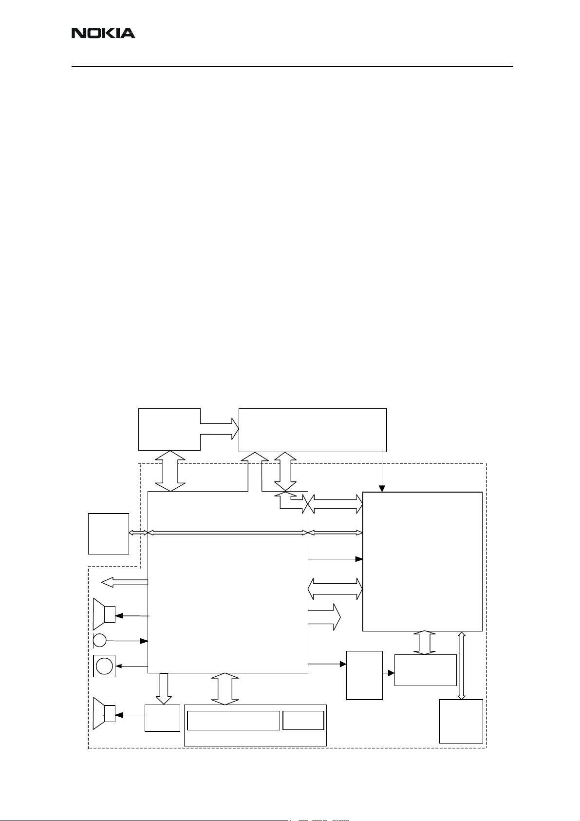
Baseband block diagram
The below system block shows the main BB function blocks.
PA Supply
UEM
SIM
Active
Cover I/F
EAR
Battery
Figure 1: Baseband block diagram
RF Supplies
UEMK
RF
RF RX/TX
Supplies
RF RX/TX
SIMIF
SLEEPCLK
32kHz
CBUS/
DBUS
BB
Clock
UPP
M
MIC
VIBRA
IHF
Audio
PA
External Audio
CI, Fbus, Vout
Charger Connection
System connector DC plug
system connector
DLIGHT
KLIGHT
Baseband
DC-
DC
Con-
verter
Keypad
Display
COMBO
Memory
Issue 3 05/2004 2004 Nokia Corporation. Page 5
Page 6

RH-19/RH-50 Company Confidential
6 - Baseband Description and Troubleshooting Nokia Customer Care
RH-19/RH-50 baseband feature list
Hardware characteristics:
• Single PWB design
• Universal Phone Processor UPP8Mv2.6 (RH-19) or UPP8Mv3.5 (RH-50) with 8Mbit
internal SRAM
• Additional external 4Mbit SRAM and 64MBit FLASH memory in one single package
(called Combo).
• Universal Energy Management ASIC UEMK (RH-19) or UEMK-edge (RH-50)
• GSM triple band 900/1800/1900 (RH-19) or 850/1800/1900 (RH-50)
• BR-5C / BL-5C battery
• Internal antenna assembled on IHF container
• Small SIM, supporting 1.8 & 3.0V
• Internal vibra motor
UI features:
• 130x130 pixel color display, 4096 colors
• Standard keypad with 4-way navigation key, two soft keys
• Illumination concept is based on a DC-DC converter
• Display: two white LED's
• Keypad: six white LED's
• Polyphonic ringing tones (MIDI)
• Internal hands-free
• Active Cover Connection
• AMR speech codec (RH-50 only)
Environmental specifications
Normal and extreme voltages
Following voltages are assumed as normal and extreme voltages for used battery:
• Nominal voltage: 3.7 V
• Lower extreme voltage: 3.2 V
• Higher extreme voltage (fast charging): 4.4 V
Temperature conditions
Operational temperature range (all specifications met within this range): -10°C..+55°C
Functional temperature range (reduced performance): -30°C..+70°C
Storage temperature range: -30°C..+85°C
Page 6 2004 Nokia Corporation. Issue 3 05/2004
Page 7
Company Confidential RH-19/RH-50
Nokia Customer Care 6 - Baseband Description and Troubleshooting
Humidity
Relative humidity range is 5.....95%.
The BB module is not protected against water. Condensed or splashed water may cause
interim or permanent phone malfunction.
Any submerge of the phone most likely causes permanent damage.
Frequencies in baseband
There are several clock frequencies at the baseband part. Below table lists all available
frequencies. The asynchronous and diagnostic busses are not included.
Table 1: Frequency list
Frequency Context UPP UEMK Flash SIM Comment
52 MHz
26 MHz
13 MHz
3.25 MHz
Up to 1 MHz
1 MHz
32 kHz
1.2 kHz
1.625 / 6.5
Memory clock
RF clock
DBUS, RFBusClk
SIM
RFConvClk
CBUS
Sleep clock
ACI
Display IF
Printed wire board (PWB)
Characteristics of the PWB
• Single PWB
• 1.2 mm, 8 layer board
• Double sided assembled
• Through holes vias and buried vias are possible
The PWB is prepared for I-Line under filling of UEMK, UPP and the Flash (64 Mbit and
128 Mbit).
X
X
XX
X
X
X
X
X
X
X
X
X
X
XMIN. FREQ.
ESTIMATION
Frequency depends on SW
Issue 3 05/2004 2004 Nokia Corporation. Page 7
Page 8

RH-19/RH-50 Company Confidential
6 - Baseband Description and Troubleshooting Nokia Customer Care
Baseband Architecture
Baseband core
Universal Phone Processor (UPP)
Main characteristics of the used UPP are:
• DSP by Texas Instruments, LEAD3 PH2+ Megacell 16 bit DSP core, 32 bit I/F - max.
speed 200 MHz.
• MCU based on ARM/Thumb 16/32 bit RISC MCU core - max. speed 50 MHz
• Internal 8 Mbit SRAM (PDRAM)
• General purpose USARTs
• SIM card interface
• Accessory interface (ACI)
• Interface control for: keypad, LCD, audio and UEMK control
• Handling of RF-BB interface
The UPP is housed in a 144-pin uBGA package (12x12mm, 0.8mm pitch).
In RH-19/RH-50 the UPP is clocked by a 26MHz frequency from the RF-chip "Mjoelner”.
This 26MHz-clock frequency is internally sliced down by UPP to 13MHz. This frequency is
then inside UPP multiplied to different frequencies, e.g. 145MHz for the DSP core.
UPP can operate on 4 different voltages; 1.05,1.3,1.5 and 1.8V. The voltage can be programmed "on the fly" by the SW. For example in standby-mode, 1.3V is used for power
saving, but in active-mode (i.e. call) the voltages is increased to 1.8V to get maximum
performance.
Universal Energy Management (UEMK)
RH-19/RH-50 uses the UEMK version so called "UEMK". UEMK is a die shrunk version of
standard UEM's, but with the same functionality.
Main characteristics of UEMK's are:
• ACI support
• Audio codec
• 11 Channel A/D converter
• Auxiliary A/D converter
• Real time logic
• Baseband regulators
• RF regulators
• Voltage references needed for analogue blocks
Page 8 2004 Nokia Corporation. Issue 3 05/2004
Page 9

Company Confidential RH-19/RH-50
Nokia Customer Care 6 - Baseband Description and Troubleshooting
• 32 kHz crystal oscillator
• SIM interface and drivers
• Security logic
• Storage of IMEI code
• Buzzer and vibra motor drivers
•2 LED drivers
• Charging function
• RF interface converters
The UEMK is housed in a 168-pin uBGA package (12x12mm, 0.8mm pitch).
External flash and external SRAM
The Combo memory is a multi chip package memory which combines 64Mbit (4Mx16)
muxed burst multi bank Flash and 4Mbit muxed CMOS SRAM. These two dies are stacked
on each other in one package. The functionality of the Flash memory is the same, as it is
known from generic BB4.0 products.
The combo is supplied by single 1.8V for read, write and erase operation.
This Combo memory is housed in a 48-ball TBGA type with a 0.5mm ball pitch. The outer
dimensions are 10x8mm and the thickness is 1.1 mm.
Energy management
The energy management of RH-19/RH-50 is based on BB 4.0 architecture. A so called
semi fixed battery (BL-5C/BR-5C) supplies power primarily to UEMK ASIC and the RF PA.
UEMK includes several regulators to supply RF and baseband. It provides the energy
management including power up/down procedure.
Power supply modes
The functional behavior of the UEMK can be divided into 7 different states. Since the
UEMK controls the regulated power distribution of the phone, each of these states
affects the general functionality of the phone:
•No supply
• Backup
•Power off
• Reset
•Power on
• Sleep
•Protection
Issue 3 05/2004 2004 Nokia Corporation. Page 9
Page 10

RH-19/RH-50 Company Confidential
6 - Baseband Description and Troubleshooting Nokia Customer Care
Figure 2: UEMK state diagram
Page 10 2004 Nokia Corporation. Issue 3 05/2004
Page 11

Company Confidential RH-19/RH-50
Nokia Customer Care 6 - Baseband Description and Troubleshooting
The text below explains the state diagram. The symbol '' means that the voltage rises
and 'Ê' that the voltage drops. '→' Means the result of the conditions set on the left
most side.
VBAT < VMSTR and VBACK > V_BUCOFF → BACK_UP
VBAT < V
VBAT V
VBAT > V
VBAT V
PWRONX = '0' or VCHAR VCHAR
VBAT > V
DELAY2 elapses → DELAY3
VBAT > C
DELAY4 elapses → PWR_ON
SLEEPX = '0' → SLEEP
SLEEPX = '1' → PWR_ON
VBAT V
No change
VBAT > V
MSTR and VBACK < V_BUCOFF → NO_SUPPLY
MSTR+ and VBACK < V_BUCOFF → DELAY1
MSTR and DELAY1 elapses → RESET
MSTR+ and VBACK > V_BUCOFF → DELAY1
DET+
or ALARM = '1' → DELAY1
COFF+ → DELAY2
OFF+. and DELAY3 elapses → DELAY4
COFF and VBAT > VMSTR- → PWR_OFF
MSTR → Stay in
PWR_OFF
PWRONX detection during
DELAY2
Watchdog elapses (approx. 100 (µs) → PWR_OFF
Thermal shutdown → PWR_OFF
PwrKeyWatchdog (4 sec.) elapses → PWR_OFF
→ PWR_OFF
The different states of the UEMK are detailed in the sections below.
Note: RH-19/RH-50 does not have a backup battery.
No Supply
In the NO_SUPPLY mode the UEMK has no supply voltage (VBAT < V
V_BU
). This mode is due to the fact that both the main battery is either discon-
COFF-
nected or discharged to a low voltage level.
The UEMK will recover from NO_SUPPLY into RESET mode if the VBAT voltage level rises
above the V
level by either reconnecting the main battery or charge it to such level.
MSTR+
and VBACK <
MSTR
Issue 3 05/2004 2004 Nokia Corporation. Page 11
Page 12

RH-19/RH-50 Company Confidential
6 - Baseband Description and Troubleshooting Nokia Customer Care
Backup
In BACK_UP mode the main battery is either disconnected or has a low voltage level
(VBAT < V
and VBACK > V_BU
MSTR-
COFF+
).
The regulator VRTC that supplies the real time clock is disabled in BACK_UP mode.
Instead the unregulated backup battery voltage VBACK supplies the output of the VRTC.
All other regulators are disabled and the phone has no functionality.
The UEMK will recover from BACK_UP mode into RESET mode if VBAT rises above V
Power Off
In order for the UEMK to be in PWR_OFF mode, it must have supply voltage (VBAT >
V
The regulator VRTC regulator is enabled and supplying the RTC within the UEMK. The
UEMK will enter RESET mode after a 20 ms delay whenever one of the below listed conditions is logically true:
• The power button is activated
• Charger connection is detected
• RTC alarm is detected
The UEMK will enter PWR_OFF from all other modes except NO_SUPPLY and BACK_UP if
the internal watchdog elapses.
Reset
When the UEMK enters RESET mode from PWR_OFF mode the watchdog is enabled. If
the VBAT fails to rise above the power-up voltage level V
dog elapses, the UEMK will enter PWR_OFF mode. Otherwise after a 200 ms delay the
regulator VFLASH1 will be enabled and after an additional delay of 500 µs the regulators
VANA, VIO, VCORE and VR3 will be enabled. All other regulators i.e. VFLASH2, VSIM, VR1,
VR2 and VR4 - VR7 are software controlled and disabled by default. After an additional
delay of 20 ms the UEMK enters PWR_ON mode.
MSTR+
.
MSTR+
).
(3.1 V) before the watch-
COFF+
Power On
In PWR_ON the UEMK is fully functional in the sense that all internal circuits is powered
up or can be by means of software. The UEMK will enter PWR_OFF mode if VBAT drops
below V
for a period of time longer than 5 µs. The UEMK will furthermore enter
COOF-
PWR_OFF mode if either of the watchdogs Operational State Machine (approx. 100 µs),
Security (32 sec.) or Power Key (4 sec.) elapses or if any of the regulators triggers the
thermal protection circuitry
Sleep
The UEMK can be forced into SLEEP mode by the UPP by setting the input SLEEPX low for
more than 60 µs. This state is entered when the external UPP activity is low (phone in
sleep) and thereby lowering the internal current consumption of the UEMK. The regulator
VANA is disabled and VR1 - VR7 are either disabled or in low quiescent mode.
Page 12 2004 Nokia Corporation. Issue 3 05/2004
Page 13
Company Confidential RH-19/RH-50
Nokia Customer Care 6 - Baseband Description and Troubleshooting
From SLEEP the UEMK enters PWR_ON if SLEEPX goes high, PWR_OFF mode if watchdog
elapses or BACK_UP mode if VBAT drops below V
MSTR-
.
Protection mode
The UEMK has two separate protection limits for over temperature conditions, one for
the charging switch and one for the regulators. The temperature circuitry measures the
on-chip temperature. In case of charging over temperature, the circuit turns the charging switch off. In case of over temperature in any of the regulators, the UEMK powers
off.
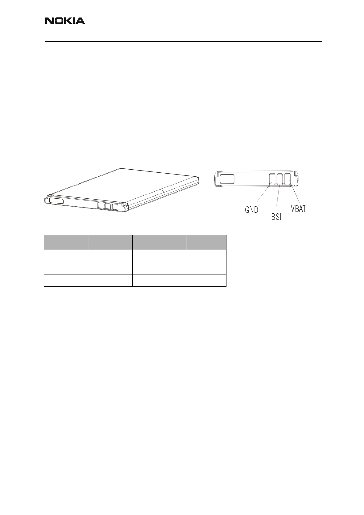
Battery BL-5C/BR-5C
Product RH-19/RH-50 uses the so called "case less" Li Ion battery BL-5C/BR-5C.
Type Capacity Manufacturer BSI Value
BL-5C 850 mAh Many sources 75 kOhm
BR-5C 820mAh Sanyo 75 kOhm
BR-5C 820mAh Matsushita 47 kOhm
Main advantage of case less battery types is the overall size, particular the thickness and
the number of contact terminals.
These batteries have a three-pin connector (BTEMP is not used). The battery does not
support temperature measurement inside battery pack. In order to get temperature
information of the battery, a NTC is mounted on the PWB within the BB area.
Ni based batteries are not supported by RH-19/RH-50.
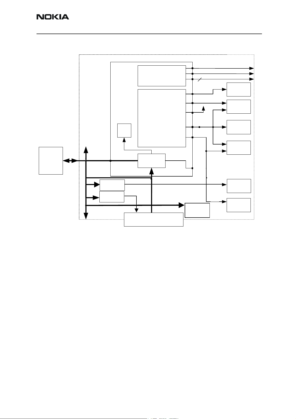
Power distribution
Under normal conditions, the battery powers the baseband module. Individual regulators
located within the UEMK regulate the battery voltage VBAT. These regulators supply the
different parts of the phone. 8 regulators are dedicated to the RF module of the phone,
and 6 to the baseband module.
The VSIM regulator is able to deliver both 1.8V and 3.0V DC and thus supporting two different SIM technologies. A register internally in the UEMK controls the output of VSIM
and can be written to by the MCU via the CBUS.
The regulator VCORE is likewise adjustable and controlled by registers written by the
Issue 3 05/2004 2004 Nokia Corporation. Page 13
Page 14

RH-19/RH-50 Company Confidential
6 - Baseband Description and Troubleshooting Nokia Customer Care
MCU. VCORE supplies the core of the UPP and can be adjusted on the fly by the MCU if
DSP capacity is inadequate. Higher VCORE supply (1.8 V) results in faster core operations
in the UPP.
The regulator VFLASH2 supplies audio circuitry and is controlled by the MCU
Regulators VANA, VFLASH1 and VIO are solely controlled by the UEMK and cannot be
enabled or disabled by the MCU. Furthermore, VFLASH1 and VIO are both ON, though in
low quiescent mode when phone is in sleep mode. An output current of 500 µA can be
drawn from the regulators. VIO supplies the UPP, FLASH and LCD, VFLASH1 supplies the
LCD module, VANA is supplying analogue parts internally in the UEMK as well as the
baseband audio circuitry and pull-up resistors on the input of the UEMK slow AD converters.
System connector provides a voltage to supply accessories. The white LED's need a higher
voltage supply as the battery can provide in bad condition. Separate external regulators
supply both consumers.
The regulators VR1A, VR1B, VR2 - VR7 and IPA1 - IPA4 are controlled by the DSP via
the DBus. VR4 - VR7 are controlled by the UEMK as well and are disabled in sleep regardless of DSP writings.
VBAT is furthermore distributed, unregulated, to the RF power amplifier, audio power
amplifier and external baseband regulators.
The CHACON module in the UEMK controls the charging of the main battery. Furthermore it contains a 3.2 Vdc regulator for charging of the backup battery and a 1.8 Vdc
regulator supplying the internal real time clock.
Page 14 2004 Nokia Corporation. Issue 3 05/2004
Page 15
Company Confidential RH-19/RH-50
r
V
Nokia Customer Care 6 - Baseband Description and Troubleshooting
Figure 3: Baseband power distribution
Battery
Baseband
UEMK
RF Regulators
Baseband
Regulators
RTC
BAT
LED
regulator
ACC
regulator
PA Supply
CHACON
VOUT
Tomahawk System Connecto
PopPortTM System Connector
VR1A
VR1B
VR2-7
VSIM
VCORE
VANA
VIO
VFLASH1
VFLASH2
6
IHF PA
SIM
UPP
FLASH
LCD
Backup
battery
LED
Keyboard/displa y
Active
Cover
Issue 3 05/2004 2004 Nokia Corporation. Page 15
Page 16

RH-19/RH-50 Company Confidential
6 - Baseband Description and Troubleshooting Nokia Customer Care
DC characteristics
The following table reflects the specifications of voltage and current regulators within
the UEMK:
Table 2: UEMK regulator outputs
Output Voltage (V) Output Current
Regulator Target
Min Typ Max Min Max
VR1A RF 4.6 4.75 4.9 0 10
(mA)
VR2
4
RF 2.70 2.78 2.86 0.1 100
VR3 RF 2.70 2.78 2.86 0.1 20
VR4 RF 2.70 2.78 2.86 0.1 50
0.1
1
VR5, VR6
RF 2.70 2.78 2.86 0.1 50
0.1
VR7 RF 2.70 2.78 2.86 0.1 45
VrefRF01 RF 1.334 1.35 1.366 - 0.1
VIO
VSIM
1
2
BB 1.72 1.8 1.88 0.005
0.005
BB 1.745
2.91
1.8
3.0
1.855
3.09
0.005
0.005
150
0.500
25
0.500
VANA BB 2.70 2.78 2.86 0.005 80
VCORE
2
BB 1.000
1.235
1.425
1.710
0.974
1.215
1.410
1.692
1.053
1.3
1.5
1.8
1.053
1.3
1.5
1.8
1.106
1.365
1.575
1.890
1.132
1.365
1.575
1.890
0.005
0.005
0.005
0.005
70
85
100
120
70
85
100
120
200
200
200
200
VFLASH1 BB 2.70 2.78 2.86 0.005
0.005
3
VFLASH2
BB 2.70 2.78 2.86 0.005 40
1
The second current value indicates the maximum possible output current of the regulator
when in low quiescent mode.
2
The output voltages are split into two different current categories. The upper part is the low-
er range of output current, and the lower part is the higher range of output current.
3
Condition in sleep-mode depends on MCU writings to UEMK regulator register solely.
4
Condition in sleep-mode depends on DSP writings to UEMK register.
70
1.5
Page 16 2004 Nokia Corporation. Issue 3 05/2004
Page 17
Company Confidential RH-19/RH-50
Nokia Customer Care 6 - Baseband Description and Troubleshooting
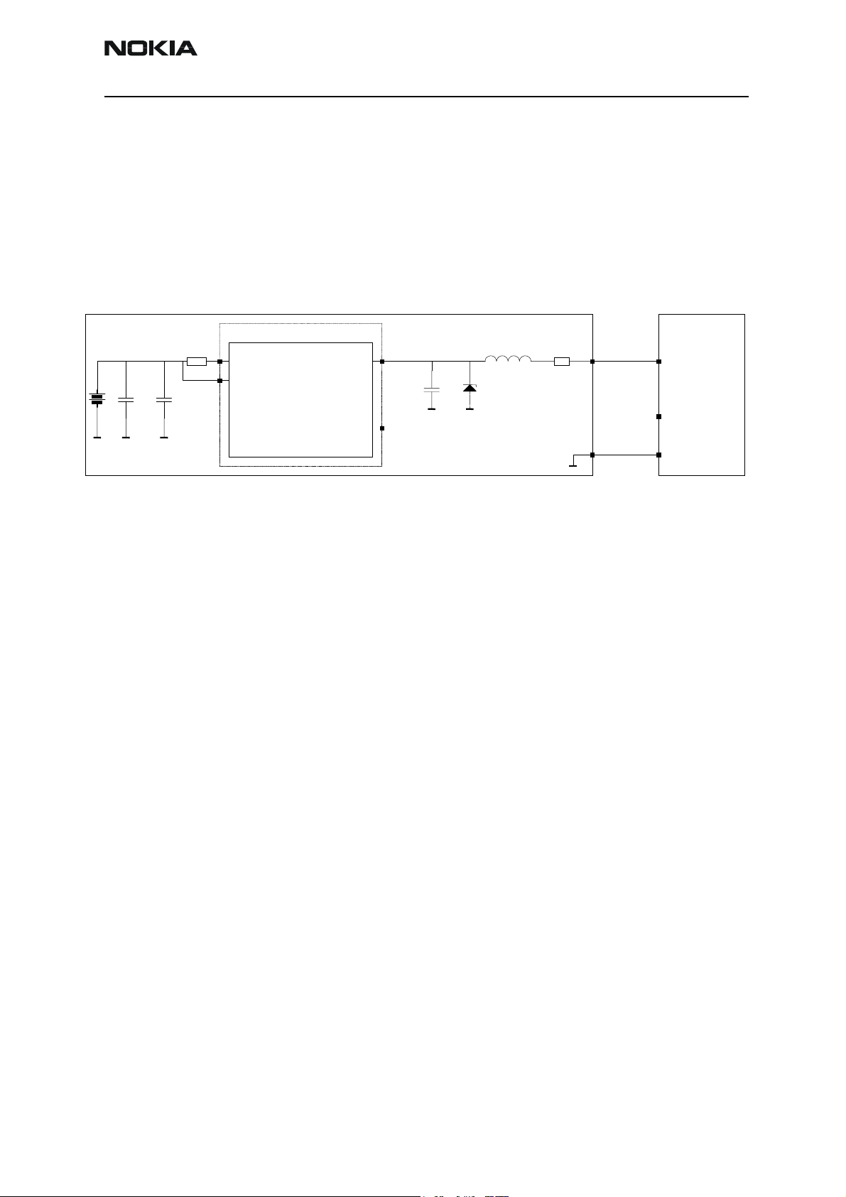
Charging
The charging of the main battery is controlled by the UEMK. External components are
needed in order to sense charging current and voltage that are needed by the Energy
Management (EM) software and to protect against EMC into the baseband area. The
charger is connected to the phone via the DCT3 bottom connector or the charger pads of
the PopPortTM system connector.
Figure 4: Charging configuration
Transceive
0R22
1u
10n
Connecting a charger to the telephone creates a voltage, VCH, on the UEMK VCHAR
input. When the VCH level is detected to rise above the VCH
CHACON, charging starts.
3-wire chargers can be connected, but the PWM is not supported.
In order to protect the phone from damage due to over voltage caused by a sudden battery removal while charging proceeds, the charger switch is closed immediately.
Audio circuitry
This section describes the audio-HW inside the BB. Thus e.g. external audio components
and acoustics are not considered with the details in this section.
UEMK
VBATREGS
CHACON
Charger
VCHARINVCHAROUT
PWM
VCHAR
1n
33R/100MHz
VCHAR
1.5A
GND
threshold (2.0 Vdc) by
DET
The main topology comes from other phones using BB4.0 engine, where the audio-HW is
mostly integrated into the UEMK-ASIC. The biggest difference is that RH-19/RH-50 has
also integrated hands-free (IHF).
Issue 3 05/2004 2004 Nokia Corporation. Page 17
Page 18
RH-19/RH-50 Company Confidential
6 - Baseband Description and Troubleshooting Nokia Customer Care
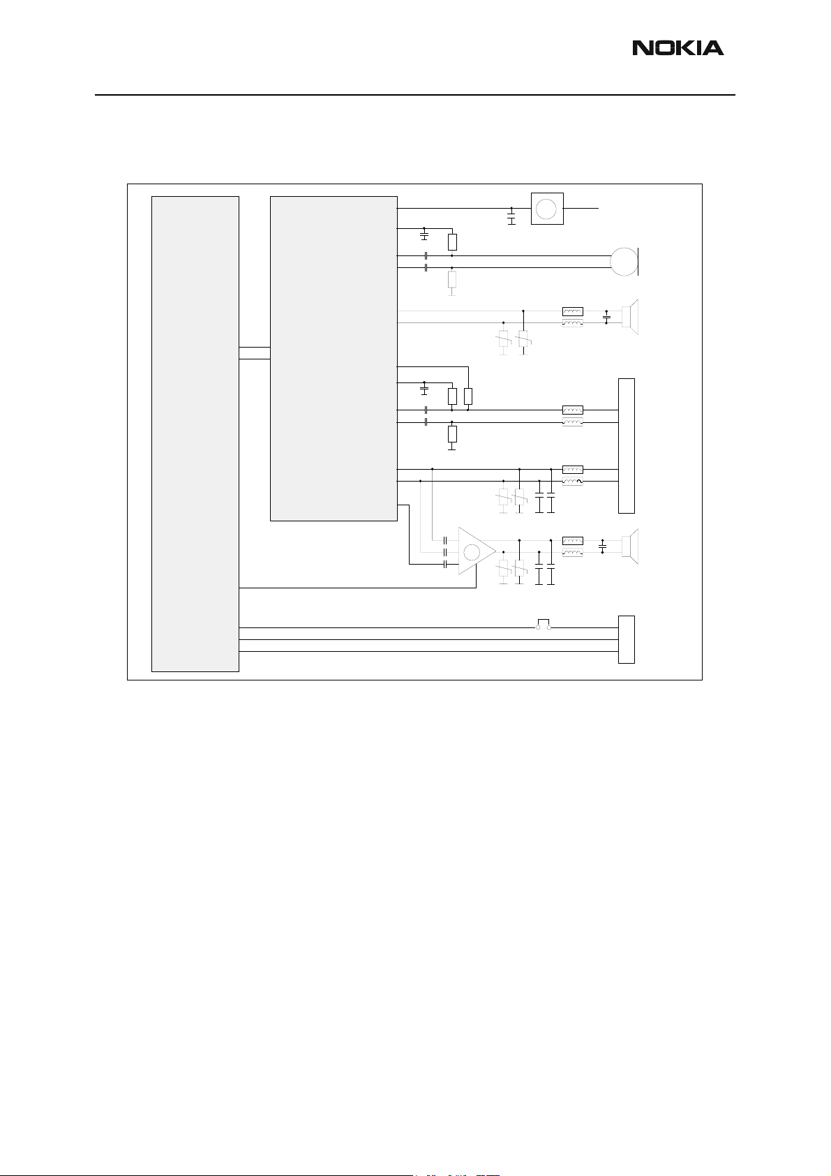
Audio block diagram
Figure 5: Audio block diagram
UPP
EARDATA
MICDATA
GENIO14
GENTEST0
FBUS_TX
FBUS_RX
UEMK
EARDATA
MICDATA
VIBRA
MICB1
MIC1P
MIC1N
EARP
EARN
HOOKINT
MICB2
MIC2P
MIC2N
HF
HFCM
XEAR
internal microphone path
earpiece path
accessory transmit path
accessory receive path
IHF speaker path
+
On/Off
IHF Amplifier
M
J103 ProdTP6
VBAT
Internal Microphone
Earpiece
XMICP
XMICN
XEARP
XEARN
Tomahawk Connector
IHF Speaker
DAI I/F
Earpiece
RH-19/RH-50 uses an earpiece which is also referred to as "PICO speaker". This is a 32
ohm speaker with the diameter of 8 mm.
Earpiece is fed by the differential signals "EARP" & "EARN" from UEMK. The signals run
quite directly from UEMK to the earpiece, only some passive ands EMC protection components are needed.
The external earpiece signals are fed by the "HF" & "HFCM" pins.
The level (swing) of earpiece-signals can be adjusted by register values inside UEMK.
These signals have common voltage level of 1.35 V (0.8 V for HF) at UEMK pins.
Microphones
An EMC-improved type of microphone is used as internal microphone in RH-19/RH-50,
diameter of which is 2.2mm.
Internal microphone circuitry is driven single ended. Microphone needs bias voltage,
Page 18 2004 Nokia Corporation. Issue 3 05/2004
Page 19

Company Confidential RH-19/RH-50
Nokia Customer Care 6 - Baseband Description and Troubleshooting
which is provided by UEMK and is fed through a resistor to the microphone. A resistor is
also needed to the other side of the microphone, i.e. between microphone and GND, in
order to provide the differential signals to UEMK. Audio signals are AC-coupled from the
microphone.
For the external microphone a differential input is used.
MIC1N & MIC1P (audio signals) and MICB1 (bias voltage) are used for the internal
microphone. MIC2N & MIC2P and MICB2 are used for external microphone.
Integrated hands-free (IHF)
The speaker used for IHF is a 16 mm diameter speaker with 8 Ohm impedance, and is also
known as "MALT" speaker.
IHF circuitry uses differential outputs from UEMK.
Depending on the audio mode the IHF amplifier is driven either from UEMK HF / HFCM or
XEAR audio outputs. The IHF audio power amplifier (APA) LM4890 has a bridge-tied-load
(BTL) output in order to get the maximum use of supply voltage. The supply voltage for
driving circuitry of speaker is VBAT, thus the swing across the speaker is ±VBAT.
The shutdown of the IHF PA is controlled by UPP using GENIO14.
Audio accessory receive path
In RH-19/RH-50 the accessory receive path is directly driven from UEMK HF / HFCM differential audio outputs, the output signal complies with the PopPortTM accessory inter-
face.
For EMC protection ferrites are connected in series to the earpiece, for ESD protection
varistors are used.
Audio control signals
Furthermore, a couple of signals are needed to control the external audio device.
The HEADINT signal is needed for recognizing the external device (e.g. headset) connected to the system. The recognition is based on the ACI-pin on the system connector,
which is shorted to ground inside the external device.
The button of the external device generates HOOKINT. This is used e.g. to answer or to
end a phone call.
Issue 3 05/2004 2004 Nokia Corporation. Page 19
Page 20

RH-19/RH-50 Company Confidential
6 - Baseband Description and Troubleshooting Nokia Customer Care
Acoustics
Earpiece acoustic
RH-19/RH-50 uses the so called "PICO" earpiece.
This earpiece is mounted into the UI-shield assembly, the sealing of the back and front
volume are implemented in the UI-shield by die casting. This sealing part also provides
the sealing against the A-cover.
Figure 6: Earpiece implementation
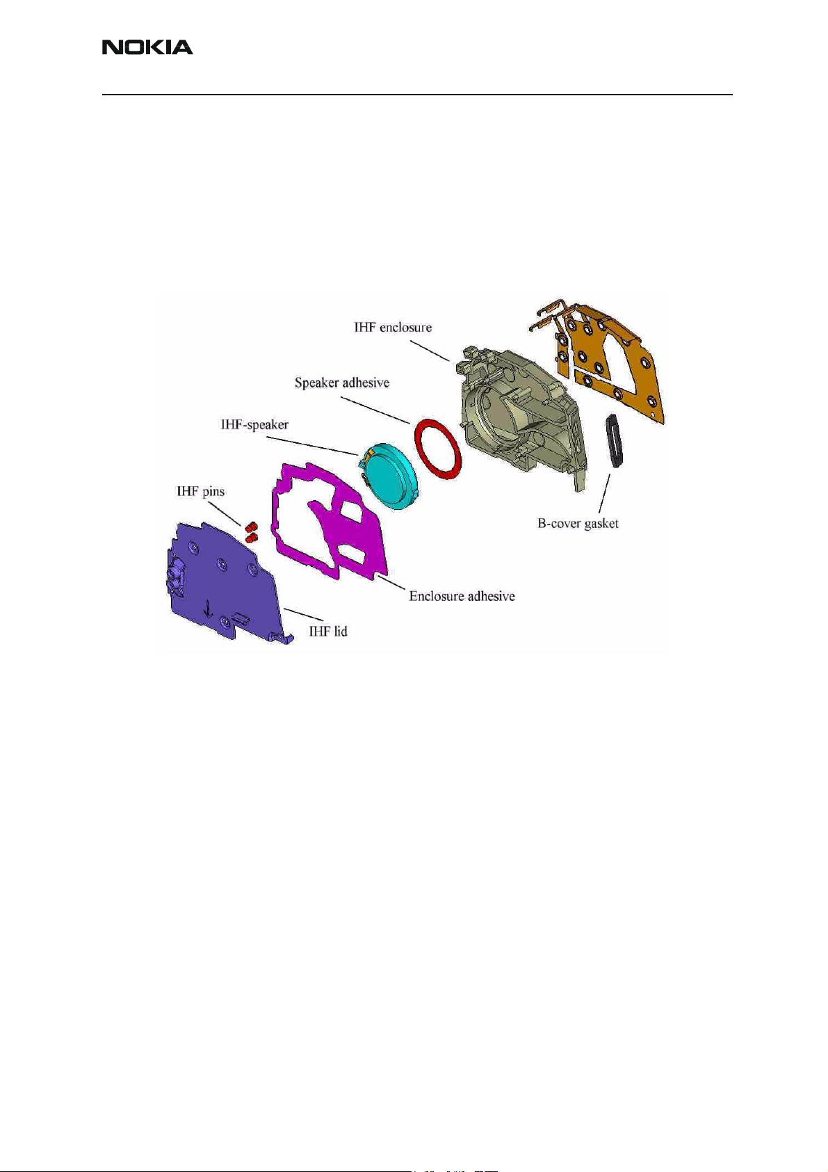
IHF speaker acoustics
As mentioned, the so called "MALT" speaker is used in RH-19/RH-50 for integrated
hands-free and ringing tone applications.
The IHF speaker is mounted to the IHF enclosure by means of the speaker adhesive. The
IHF enclosure provides the needed back volume for the speaker. The IHF enclosure is
closed with the IHF lid, which is carrying the IHF pins to contact the IHF speaker.
The sealing of the effective acoustic volumes is achieved with the enclosure adhesive,
which glues the IHF lid to the IHF enclosure.
To provide a long-term reliability additionally the IHF lid is heat stacked to the IHF enclosure.
The B-cover gasket provides a fitting between the B-cover and the IHF enclosure. This
fitting is attached with an adhesive to the IHF enclosure and also includes a dust and
Page 20 2004 Nokia Corporation. Issue 3 05/2004
Page 21
Company Confidential RH-19/RH-50
Nokia Customer Care 6 - Baseband Description and Troubleshooting
water shield to protect the speaker inside from dust and swarf.
Due to the fact that the IHF enclosure is also carrying the antenna radiator, the whole
assembly is named antenna assembly.
Due to heat stacking of the antenna assembly, it cannot be disassembled and in case of
failure only be exchanged as one complete assembly.
Figure 7: Exploded view of antenna assembly
Microphone acoustics
A standard microphone module is used. This module is embedded into a so called "rubber
boot" and connected to RH-19/RH-50 system module by spring contacts.
The microphone is placed close to the system connector. The sound port of the microphone is located towards the bottom of the phone
Vibra motor
A vibrating alerting device is used to generate a vibration signal for an incoming call.
This vibra is located in the bottom section of the phone.
The vibrator is driven by the UEMK output VIBRA, and controlled with a PWM signal. The
supply of the vibra is taken from the battery voltage of the phone.
Issue 3 05/2004 2004 Nokia Corporation. Page 21
Page 22

RH-19/RH-50 Company Confidential
6 - Baseband Description and Troubleshooting Nokia Customer Care
Audio modes
There are six different audio configurations. These can create following audio modes:
•Hand portable
• Integrated hands-free
• Headset
• Loop set
• External hands-free
The following audio sources have to be routed according to the active audio mode:
• Speech
• Ringing tones / SMS tones
• Keypad tones
• Error tones / Warning tones
• Game tones
Hand portable mode
In hand portable mode earpiece path and internal microphone path are in use. The audio
sources are routed according to the following table:
Table 3: Handportable mode audio routing
Audio Source Earpiece
Speech X X
Ringing tones, SMS tones X
Keypad tones X
Warning / Error tones X
Game tones X
Internal
Microphone
IHF
speaker
Accessory
receive path
Accessory
transmit path
Page 22 2004 Nokia Corporation. Issue 3 05/2004
Page 23

Company Confidential RH-19/RH-50
Nokia Customer Care 6 - Baseband Description and Troubleshooting
Integrated hands-free audio mode
In integrated hands-free mode IHF path and internal microphone path are used. The
audio sources are routed according to the following table:
Table 4: IHF mode audio routing
Audio Source Earpiece
Speech X X
Ringing tones, SMS tones X
Keypad tones X
Warning / Error tones X
Game tones X
Internal
Microphone
Headset audio mode
In headset mode accessory receive path and accessory transmit path are used. RH-19/
RH-50 supports the following headsets:
• HDB-4: mono headset, boom design
• HS-1C: camera headset
• HS-10: retractable headset
• HSU-3: privacy headset
• HS-5: mono headset traditional design (RH-50 only)
• HS-2R: FM radio headset (RH-50 only)
IHF
speaker
Accessory
receive path
Accessory
transmit path
The audio sources are routed according to the following table:
Table 5: Headset mode audio routing
Audio Source Earpiece
Speech X X
Ringing tones, SMS tones X X
Keypad tones X
Warning / Error tones X
Game tones X
Internal
Microphone
IHF
speaker
Accessory
receive path
Loop set audio mode
In loop set mode accessory receive path and accessory transmit path are used. RH-19/
Accessory
transmit path
Issue 3 05/2004 2004 Nokia Corporation. Page 23
Page 24
RH-19/RH-50 Company Confidential
6 - Baseband Description and Troubleshooting Nokia Customer Care
RH-50 supports the loop set LPS4.:
Table 6: Loop set mode audio routing
Audio Source Earpiece
Speech X X
Ringing tones, SMS tones X X
Keypad tones X
Warning / Error tones X
Game tones X
Internal
Microphone
IHF speaker
Accessory
receive path
External hands-free audio mode
In external hands-free mode accessory receive path and accessory transmit path are
used. RH-19/RH-50 supports external hands-free accessories:
BHF-1: basic car hands-free kit
HFU-4: advanced car hands-free kit
Table 7: External hands-free mode audio routing
Audio Source Earpiece
Internal
Microphone
IHF speaker
Accessory
receive path
Accessory
transmit path
Accessory
transmit path
Speech X X
Ringing tones, SMS tones X
Keypad tones X
Warning / Error tones X
Game tones X
Page 24 2004 Nokia Corporation. Issue 3 05/2004
Page 25

Company Confidential RH-19/RH-50
Nokia Customer Care 6 - Baseband Description and Troubleshooting
User Interface
LCD module
RH-19/RH-50 is using a 130 * 130 dot LCD display with 4096 colors. The illumination is
integrated into the LCD module.
Baseband-LCD interface
The LCD display is connected to the transceiver PWB by 10-pin board-to-board connector.
Figure 8: LCD connector
1
10
DC characteristics
Display is using 3-wire serial interface. Signals for LCD panel are shown in table below.
The chip-select XCS (active low) enables and disables the serial interface. RESX (active
low) is external reset signal. The SCL is serial data clock. SI data-length is 8 bits + D/Cbit. First bit is D/C-bit which indicates the status of following 8 bit data. In case of command data D/C-bit is low ('0'). VDDI is logic voltage supply for the display. VDD is supply
voltage for high voltage generation. GND is system ground for display.
Issue 3 05/2004 2004 Nokia Corporation. Page 25
Page 26

RH-19/RH-50 Company Confidential
6 - Baseband Description and Troubleshooting Nokia Customer Care
Table 8: LCD Interface DC characteristics
Pin No Signal name Description Min Typical Max Unit Description
1 VDDI IN 1.7 1.8 VDD V Logic voltage supply
2 RESX IN H: 0.7xVDD
L: 0
3SI IN H: 0.7xVDDI
L: 0
4 SCL IN H: 0.7xVDDI
L: 0
5 XCS IN H: 0.7XVDDI
L: 0
6 VDD IN 2.6 2.75 3.6 V Voltage supply
7 NC 0 V Not connected
8 GND System ground
9 LED - 0.505 0.525 0.545 V
10 LED + TBD 7.0 TBD V
Note: H stands for high signal level and L for low signal level.
H: VDDI
L: 0.3xVDDI
H: VDDI
L: 0.3xVDDI
H: VDDI
L: 0.3xVDDI
6.5 MHz Serial data clock speed
H: VDDI
L: 0.3xVDDI
V Reset
(active low)
V Serial input
V Serial input clock
V Chip select
(Active low)
Page 26 2004 Nokia Corporation. Issue 3 05/2004
Page 27

Company Confidential RH-19/RH-50
Nokia Customer Care 6 - Baseband Description and Troubleshooting
Current consumption
Table 9: LCD interface current consumption
Pin
Signal name Description Min Typical Max Unit Description
No.
6/8 VDD Display pixels - 0.5 1.25 mA Full mode, 4 k colors. Maximum
for chess pattern picture.
6/8 VDD Display pixels - 0.15 0.25 mA Partial mode, 32 lines, 4 k colors.
Maximum for chess pattern picture
9/10 LED - LED + Display illumination - 15 30 mA 2 white LED in series
Maximum ratings
Table 10: LCD interface maximum ratings
Item Symbol Rating Unit
Power Supply voltage V
Power supply voltage (logic) V
Signal Input voltage V
LED input current I
AC characteristics
DD
DDI
IN
LED
Figure 9: Write characteristics
-0.3 to + 4.0 V
-0.3 to + 4.0 V
-0.3 to Vddi + 0.5 V
30 mA
Issue 3 05/2004 2004 Nokia Corporation. Page 27
Page 28

RH-19/RH-50 Company Confidential
6 - Baseband Description and Troubleshooting Nokia Customer Care
Table 11: AC characteristics
Signal Symbol Parameter Min Max Unit
CSX T
SCL t
SI T
CSS
T
CSH
SCYC
t
SLW
t
SHW
SDS
T
SDH
Chip select setup time 10 - ns
Chip select hold time 35 - ns
Clock cycle 150 - ns
Clock pulse "L" duration 60 - ns
Clock pulse "H" duration 60 - ns
Data setup time 60 - ns
Data hold time 60 - ns
1. Rise tr and fall tf time must be within 15 ns maximum.
2. Timings are specified according to 30% and 70% of V
rise and fall times are described in the figure below.
Figure 10: Rise and fall time input and output
tr
70%
tf
70%
as reference. Definitions to
DDI
30%
30%
Table 12: Rise and fall times in input and output of display driver
Parameter Symbol Min Max Unit
Input Tr, tf 15 ns
Output Tr, tf 15 ns
Page 28 2004 Nokia Corporation. Issue 3 05/2004
Page 29

Company Confidential RH-19/RH-50
Nokia Customer Care 6 - Baseband Description and Troubleshooting
Reset timing
Reset timing characteristics are shown in the figure below.
Figure 11: Reset timing
Table 13: Reset Timing
Signal Symbol Parameter Min Max Unit
RESX tRW Reset pulse duration 200 ns
tRT Reset cancel 1500 ns
Display power on/off sequence
Power on/off sequence if described in the figure below.
VDDI
VDD
CSX
RESX
t<1ms
t>100ns
Figure 12: Power on/off sequence
t<1ms
Issue 3 05/2004 2004 Nokia Corporation. Page 29
Page 30

RH-19/RH-50 Company Confidential
6 - Baseband Description and Troubleshooting Nokia Customer Care
LED power supply
In RH-19/RH-50, white LED are used for LCD and for keypad lighting. Two LED are used
for LCD lighting and six LED for keyboard. A step up DC-DC converter TK11851 is used as
a LED driver.
Display Module
DCDC-Converter
Vbat
TK11851
Keypad
Shutdown
(DLIGHT)
Vfb
RRR
Keypad LEDs
Ricd
The display LEDs are driven in serial mode to achieve stable backlight quality. This means
constant current flow through LCD LEDs. Serial resistance R_lcd is used to define the
proper current. The feedback signal, FB, is used to control the current. Driver will increase
or decrease the output voltage for LEDs to keep the current stable.
Keyboard LED are driven in 2 serial/3 parallel mode. This means constant current flow
through each branch. Serial resistance R are used to limit the current through LEDs.
Driver is controlled by the UEMK via the DLIGHT open drain output (internal pull up
active). This signal is connected to driver EN-pin. It is possible to control the LED brightness by PWM.
The RH-19/RH-50 phone doesn't have separate keyboard PCB. The keys are directly connected via the KEYB(10:0) bus to the UPP. The keypad consist of a 5x4 matrix, meaning 5
rows (ROW0 - ROW4) and 4 columns (COL1 - COL4).
Page 30 2004 Nokia Corporation. Issue 3 05/2004
Page 31

Company Confidential RH-19/RH-50
Nokia Customer Care 6 - Baseband Description and Troubleshooting
Figure 13: RH-19/RH-50 key pad
Within the RH-19/RH-50 design, there was a requirement to allow the use of multiple
keys to be operated at a time, for use with games etc. Thus the keypad can be operated
in this manner.
The power on key is connected to the UEMK PWRONX signal.
Issue 3 05/2004 2004 Nokia Corporation. Page 31
Page 32

RH-19/RH-50 Company Confidential
6 - Baseband Description and Troubleshooting Nokia Customer Care
SIM Interface
RH-19/RH-50 uses the same SIM card reader (SIM reader) as the NPL-2. Electrical connection of SIM reader is similar to other DCT4 products.
The SIM interface is split between UEMK and UPP (see figure below). This has been done
in order to reduce the amount of interconnections on the SIM interface between the UPP
and the UEMK.
The SIM interface control logic and UART is integrated into the UPP. The SIM interface
start-up and power down sequence, including timing and reset generation is implemented in UEMK. The SIM interface in the UPP supports the SIM speed enhancement
features, which improves the data transfer rate in the SIM interface.
The UEMK contains the SIM interface logic level shifting. UPP SIM interface logic levels
are 1.8V. The SIM interface can be programmed to support 3V and 1.8V SIMs. A 5V SIM
interface is not supported. A register in the UEMK selects the SIM supply voltage. It is
only allowed to change the SIM supply voltage when the SIM IF is powered down.
The SIM power up/down sequence is generated in the UEMK. The Battery Size Indication
(BSI) is used to recognize if the battery suddenly is removed from the transceiver block.
The SIMCardDet is not used. If the BSI goes low, the power down sequence is automatic
initiated. The SIMIF will then force all the connections low, i.e. SIMRST, SIMCLK, SIMDATA and VSIM. A comparator inside the UEMK does the monitoring of the BSI signal.
The comparator offset is such that the comparator output does not alter state as long as
the battery is connected. The BSI comparator threshold level is 2.1 V with 75 mV hysteresis.
Figure 14: UPP, UEMK and SIM connections
K
Page 32 2004 Nokia Corporation. Issue 3 05/2004
Page 33

Company Confidential RH-19/RH-50
Nokia Customer Care 6 - Baseband Description and Troubleshooting
BB-RF Interface
The below table describes all the signals from the baseband block to the RF block and
back. The signal names are based on the schematics.
Digital signals between BB and RF
For the digital interfaces UPP and Mjoelner use only level shifting IO. Level shifters of
both are supplied with VIO from UEMK. VIO limits are specified in chapter 5.3 and have
been used to calculate the limits below (because VIO
V
and not the limit from UPP which would have been 1.26V).
DDSmin
Values are referenced to GND unless otherwise specified.
Table 14: RF-BB interface digital signals
Signal name From To Parameter Min Typ Max Unit Notes
RFICCNTRL (2:0) Mjoelner control bus
is 1.72V this was used for UPP
min
RFBUSEN1
RFICCNTRL(2)
RFBUSDA
RFICCNTRL(1)
RFBUSCLK
RFICCNTRL(0)
UPP
RFBUSEN1
X
UPP
RFBUSDA
UPP
RFBUSCLK
Mjoelner
RFBUSENX
Mjoelner
RFBUSDA
Mjoelner
RFBUSCLK
Logic
"1"
Logic
"0"
Logic
"1"
Logic
"0"
Logic
"1"
Logic
"0"
Clock Speed 13 MHz
Mjoelner input
UPP output
Mjoelner input
UPP output
Mjoelner input
UPP output
Mjoelner output
UPP input
Mjoelner input
UPP output
Mjoelner output
UPP input
Mjoelner input 1.22 V RF bus clock.
UPP output 1.37 1.88 V
Mjoelner input 0 0.4 V
UPP output 0 0.40 V
1.22
1.37 1.88VV
0
0
1.22
1.37
1.32
1.32
0
0
0
0
0.4
0.40VV
1.88
1.88
0.4
0.40
0.4
0.51
V
V
V
V
V
V
V
V
RF Chip select.
Active Low
RF serial data.
(bi-directional)
RF serial data.
(bi-directional)
GENIO (28:0) General purpose I/O
TXP
GENIO(5)
UPP
GENIO5
Mjoelner
TXP
Logic
"1"
Logic
"0"
Mjoelner input 1.22 V Transmitter
UPP output 1.37 1.88 V
Mjoelner input 0 0.4 V
UPP output 0 0.40 V
power control
enable.
Issue 3 05/2004 2004 Nokia Corporation. Page 33
Page 34

RH-19/RH-50 Company Confidential
6 - Baseband Description and Troubleshooting Nokia Customer Care
Table 14: RF-BB interface digital signals
Signal name From To Parameter Min Typ Max Unit Notes
RESET
GENIO(6)
UPP
GENIO6
Mjoelner
RESET
Logic
"1"
Logic
"0"
Mjoelner input 1.22 V Reset to RF
UPP output 1.37 1.88 V
Mjoelner input 0 0.4 V
UPP output 0 0.40 V
chip.
Active low.
Page 34 2004 Nokia Corporation. Issue 3 05/2004
Page 35

Company Confidential RH-19/RH-50
Nokia Customer Care 6 - Baseband Description and Troubleshooting
Analog signals between BB and RF
The values indicated in the table below are input requirements of the device in the "to
column" when nothing else is stated. Values are referenced to GND unless other wise
specified.
Table 15: RF-BB interface analog signals
Signal name From To Parameter Min Typ Max Unit Notes
Clock System clock for phone
RFCLK Mjoelner
REFOUT
RFCONV (9:0) RF / BB analogue signals
RXIINP
RFCONV(0)
RXIINN
RFCONV(1)
RXQINP
RFCONV(2)
RXQINN
RFCONV(3)
TXIOUTP
RFCONV(4)
TXIOUTN
RFCONV(5)
TXQOUTP
RFCONV(6)
TXQOUTN
RFCONV(7)
Mjoelner
RXIP
Mjoelner
RXIM
Mjoelner
RXQP
Mjoelner
RXQM
UEMK
TXIOUTP
UEMK
TXIOUTN
UEMK
TXQOUTP
UEMK
TXQOUTN
UPP
RFCLK
UEMK
RXIINP
UEMK
RXIINN
UEMK
RXQINP
UEMK
RXQINN
Mjoelner
TXIP
Mjoelner
TXIN
Mjoelner
TXQP
Mjoelner
TXQN
Frequency 26 MHz System clock
Duty cycle 40 60 %
Signal amplitude 0.3 1.32 Vpp Upp input req.
Setling time 5.0 ms VR3 on to sta-
Max input
Voltage swing
Nominal Voltage swing V
Input DC level 1.3 1.35 1.4 Vdc
Signal frequency 67,7 KHz
Input BW 270.83KHz
Max Differential output
swing (ref. TxIN)
Input diff. Swing
(ref. TxIN)
DC level 1.0 1.1 1.25 Vdc
Source impedance 200 W
Signal frequency 67,7 KHz
-20 +20 ppm
ble clock @
UPP input
1.35 1.4 1.45 Vpp Differential
complex RX
BB signal
2.15 2.2 2.25 Vpp Differential
complex TX
1.0 Vpp
signal (programmable
voltage swing)
RFAUXCONV(2:0) RF / BB analogue control signals
Issue 3 05/2004 2004 Nokia Corporation. Page 35
Page 36

RH-19/RH-50 Company Confidential
6 - Baseband Description and Troubleshooting Nokia Customer Care
Table 15: RF-BB interface analog signals
Signal name From To Parameter Min Typ Max Unit Notes
TXC
RFAUXCONV(0)
UEMK
AUXOUT
Mjoelner
TXC
Output voltage 0 -
0.1
Source impedance 200 W
Resolution 10 Bits
Reference Auxref
(VrefRF01
?)
Power coef. Range. 0,05 0,94 Vtxc/
Recom. Power Coef.1 @
pwr.lvl.5 (0 pcn)
Recom.Power Coef. @
pwr.lvl.19 (15 pcn)
Recom.Power Coef @
Base level
0,7 0,9 Vtxc/
0,1 0,2 Vtxc/
0,1 0,2 Vtxc/
2,4 -
2.55
VTransmitter
Vtxc_m
ax
Vtxc_m
ax
Vtxc_m
ax
Vtxc_m
ax
power control
Page 36 2004 Nokia Corporation. Issue 3 05/2004
Page 37

Company Confidential RH-19/RH-50
Nokia Customer Care 6 - Baseband Description and Troubleshooting
Voltage regulators in BB for RF
Values are referenced to GND unless otherwise specified.
Table 16: Voltage supplies and references
Signal name From To Parameter Min Typ Max Unit Notes
Regulators RF regulators
VR1A UEMK
VR1A
VR2 UEMK
VR2
VR3 UEMK
VR3
Mjoelner
VDDCP
Mjoelner
VDDTX
VDDDIG
Mjoelner
VDDXO
VDDBBB
UEMK Output Voltage 4.6 4.75 4.9 V Supply to :
Mjoelner Input Voltage 2.64 2.78 4.9 V
UEMK output Load Current
UEMK Load Capacitance 800 1000 1200
Settling Time 300+t
UEMK Output Voltage 2.70 2.78 2.86 V Supply to TX -
Mjoelner Input Voltage 2.64 2.78 2.86 V
Load Current 0.1 3) 100 mA
Load Capacitance 800 1000 1200
Settling Time 10 µs Sleep to
UEMK Output Voltage 2.70 2.78 2.86 V Supply to :
0(3) 5 mA
nF
(4)
20 600 mΩ ESR
d
2
(4)
20 600 mΩ ESR
µs Sleep to
nF
Charge pump
Active
chain Modulator digital
contl logic
Active
XO and baseband buffer
VR4 UEMK
VR4
Mjoelner
VDDRXBB
Mjoelner Input Voltage 2.64 2.78 2.86 V
Load Current 0.1 (3) 20 mA
Load Capacitance 800 1000 1200
(4)
20 600 mΩ ESR
Settling Time 100 µs Off to on
10 ? µs Sleep to
UEMK Output Voltage 2.70 2.78 2.86 V Supply to :
Mjoelner Input Voltage 2.64 2.78 2.86 V
Load Current 0.1 (3) 50 mA
nF
Active
RX baseband
section
Issue 3 05/2004 2004 Nokia Corporation. Page 37
Page 38

RH-19/RH-50 Company Confidential
6 - Baseband Description and Troubleshooting Nokia Customer Care
Table 16: Voltage supplies and references
Signal name From To Parameter Min Typ Max Unit Notes
VR5 UEMK
VR5
Mjoelner
VDDPRE
VDDLO
VDDPLL
UEMK Output Voltage 2.70 2.78 2.86 V Supply to :
Mjoelner Input Voltage 2.64 2.78 2.86 V
Load Current 0.1 (3) 50 mA
Load Capacitance 800 1000 1200
(4)
nF
Prescaler,
deviders,
LO buffers, PLL
counters
20 600 mΩ ESR
Settling Time 10 µs Sleep to
Active
VR6 UEMK
VR6
Mjoelner
VDDRXF
UEMK Output Voltage 2.70 2.78 2.86 V Supply to :
Mjoelner Input Voltage 2.64 2.78 2.86 V
RX frontend
Load Current 0.1 (3) 50 mA
Load Capacitance 800 1000 1200
(4)
nF
20 600 mΩ ESR
Settling Time 10 µs Sleep to
Active
VR7 UEMK VCO UEMK Output Voltage 2.70 2.78 2.86 V Supply to :
VCO supply voltage
2
range
2.55 2.78 2.85 V
VCO
Load Current 0.1 (3) 45 mA
Load Capacitance 800 1000 1200
Settling Time 10 µs Sleep to
VIO UEMK
VIO
Mjoelner
VDDDL
UEMK Output Voltage 1.72 1.88 1.88 V Supply to:
Mjoelner Input Voltage 1.71 1.8 1.88 V
Load Current 0.1 (3)
Load Capacitance
Settling Time
References RF References
nF
(4)
20 600 mΩ ESR
Active
RF-BB interface level
(3)
5
mA
shifter
Page 38 2004 Nokia Corporation. Issue 3 05/2004
Page 39

Company Confidential RH-19/RH-50
Nokia Customer Care 6 - Baseband Description and Troubleshooting
Table 16: Voltage supplies and references
Signal name From To Parameter Min Typ Max Unit Notes
VREF1 UEMK
VREF01
Mjoelner
VBEXT
UEMK Output Voltage 1.3341.35 1.366 V Used inside
MJOELNER as
Mjoelner Input Voltage 1.3251.35 1.375 V
Load Current (3) 100 mA
Load Capacitance 800 1000 1200
(4)
Settling Time µs Sleep to
nF
1.35V reference
Active
Issue 3 05/2004 2004 Nokia Corporation. Page 39
Page 40

RH-19/RH-50 Company Confidential
6 - Baseband Description and Troubleshooting Nokia Customer Care
System Connector Interface
System connector
The system connector in RH-19/RH-50 (and several other DCT-4 products) is called PopPortTM system connector. It is a galvanic interface between phone and accessories.
Compared with previous system connector versions, four new functions are introduced
with the PopPortTM system connector interface:
• Accessory Control Interface (ACI)
•Power Out
• Stereo audio output
• Universal Serial Bus (USB).
USB functionality and stereo audio output of the Pop-port are not supported in RH-19/
RH-50.
Note: MBUS function, (included in previous accessory interfaces, e.g. DCT-3) is no more supported by PopPort
interfaces.
PopPortTM system connector is mechanically and electrically not backward compatible
with any earlier Nokia accessory interfaces, except the charger connector.
Figure 15: PopPortTM system connector
ACI
Vout
Charge
Charge GND
Shielding GND
Fbus TX
Fbus RX
DATA GND
XMIC P
XMIC N
HSEAR P
HSEAR N
Shielding GND
Page 40 2004 Nokia Corporation. Issue 3 05/2004
Page 41

Company Confidential RH-19/RH-50
Nokia Customer Care 6 - Baseband Description and Troubleshooting
Table 17: System connector interface description
Pin # Signal Notes
1VCHAR
2 GND Charge ground
3 ACI Insertion & removal detection /
Serial data bi-directional 1 kbit/s
4Vout
5 Not used in RH-19/RH-50
6 FBUS_RX Serial data from accessory to phone / 115 kbit/s
7 FBUS_TX Serial data from phone to accessory / 115 kbit/s
8 GND Data ground
9 XMIC N Negative audio in signal
10 XMIC P Positive audio in signal
11 HSEAR N Negative audio out signal.
Max bandwidth from the phone
12 HSEAR P Positive audio out signal.
Max bandwidth from the phone
13 Not used in RH-19/RH-50
14 Not used in RH-19/RH-50
Accessory control interface (ACI)
ACI is a point-to-point, master-slave, and bi-directional serial bus. It has three features:
• The insertion and removal detection of an accessory device
• Acting as a data bus, intended mainly for control purposes
• The identification and authentication of accessory type which is connected
The accessories are detected by the HeadInt signal when the plug is inserted.
Normally, when no plug is present, the pull-up resistor 100k pulls up the HeadInt signal
to VFLASH1. If the accessory is inserted, the external "insertion & removal" resistor works
as voltage divider and decrease the voltage level below the threshold Vhead.
Thereby the comparator output will be changed to high state causing an interrupt.
If the plug is removed, the voltage level of HeadInt increases again to VFLASH1. This
voltage level is higher than the threshold of the comparator and thereby its output will
be changed to low. These changes lead to an interrupt.
These HeadInt interrupts are initiated the accessory detection or removal sequence.
TM
If no accessory inserted / connected the only active part on the PopPort
interface is
Issue 3 05/2004 2004 Nokia Corporation. Page 41
Page 42

RH-19/RH-50 Company Confidential
6 - Baseband Description and Troubleshooting Nokia Customer Care
the ACI line.
Figure 16: Principle schematics of ACI accessory and engine
Signal flow on ACI line - ACI-ASIC accessory inserted
Figure 17: ACI communication
V
headInt
V
FLASH1
V
head_min
V
aci_detect
1
V
high
V
low
2
a
2
1
a
RESET
4
3
Learning Sequence
5
1. Accessory is connected (insertion & removal resistor connect to ACI line)
1a) phone gets HeadInt interrupt after 20ms check that ACI line is still low (<Vhead min)
2. Connect MBUS with HeadInt line (MBUS switch)
2a) If the phone detect a HeadInt interrupt from low to high transition in 20ms timeframe, then an advanced accessory is connected
Normal
ACI communication
7
6
9
a
9
8
3. ACI chip reset (3000- 4000us)
4. Power up delay (50-400us)
5. Start bit (50us)
Page 42 2004 Nokia Corporation. Issue 3 05/2004
Page 43

Company Confidential RH-19/RH-50
Nokia Customer Care 6 - Baseband Description and Troubleshooting
6. Learning sequence (567-1700us)
7. ACI communication
8. MBUS is disconnected from HeadInt line (MBUS switch). After every communication.
9. Accessory is removed (no insertion & removal resistor on ACI line) --> phone gets
HeadInt interrupt from ACI line low to high transition.
9a) If no HeadInt interrupt comes in the next 100ms the accessory is really removed and
the phone goes in the state "no accessory".
Table 18: Voltage Levels
Signal Min Typ Max Unit Note
V
FLASH1
V
head
Specified values
for levels
V
ACI_detect
2.7 2.78 2.86 V
1.75 1.9 2.05 V
Min Typ Max Unit Note
0.83 1.13 V Voltage level if MBUS not connected
to HeadInt (MBUS switch open), but
ACI accessory is inserted.
V
high
2.45 2.71 V Voltage level after MBUS connected to
HeadInt.
V
low
<0.22*VDD V
Signal flow on ACI line - Non ACI-ASIC accessory inserted
Figure 18: Signal flow on ACI line
V
headInt
V
FLASH1
V
head_m in
1
20ms
2
1
a
V
low
3
Mono Headset is
recognized.
3
a
4
a
4
1. Accessory is connected (insertion & removal resistor connect to ACI line)
1a) phone gets HeadInt interrupt after 20ms check that ACI line is still low (<Vhead min)
2. Connect MBUS with HeadInt line (MBUS switch)
3. The 20 ms timer elapsed and no transition has been on HeadInt line
3a) Disconnect MBUS from HeadInt line
Issue 3 05/2004 2004 Nokia Corporation. Page 43
Page 44

RH-19/RH-50 Company Confidential
6 - Baseband Description and Troubleshooting Nokia Customer Care
4. Accessory is removed. Phone gets HeadInt interrupt from ACI line low to high transition.
4a) If no HeadInt interrupt comes in the next 100ms the accessory is really removed.
FBUS
FBUS is an asynchronous data bus with separate TX and RX signals. Default bit rate of
the bus is 115.2 Kbit/s.
FBUS is used as additional communication channel from phone to accessory and vice
versa. There is two types of accessories which it uses:
1. Nokia Serial Bus Accessory, AT mode
2. Fbus Phonet mode accessory
From HW-point of view, this does not make any difference.
Table 19: FBUS interface
Signal Parameter Min Typ Max Unit
FBUS_RX V
FBUS_TX V
IH
V
IL
OH
V
OL
1.95 2.78 3.0 Volt
0 0.2 0.83
1.95 2.78 2.83
0 0.2 0.83
VOUT (Accessory Voltage Regulator)
DCT4 chip set does not provide and power supply for accessories. To enable this an external LDO regulator is needed. This regulator is called "Accessory Regulator".
The regulator input is connected directly to battery voltage VBAT and the output to VOUT
pin at system connector. The regulator is controlled by the GENIO(0) line of UPP. With
this signal the regulator can be switched on and off.
The regulator can be supply up to150 mA.
Note: This exceeds the PopPortTM minimum requirement.
Page 44 2004 Nokia Corporation. Issue 3 05/2004
Page 45

Company Confidential RH-19/RH-50
Nokia Customer Care 6 - Baseband Description and Troubleshooting
Figure 19: Accessory power supply diagram
TM
VOUT
0.9R
UPP
GenIO(0)
VBAT
Voltage
regulator
En
LP3985
Tomahawk
PopPort
bottom connector
DC resistance of ferrite
+ impedance of line and connector
Table 20: Accessories Power Supply
Signal Min Nom Max Unit Note
Vout
GenIO(0) 1.4 1.88
2.63
2,56
2.80 2.88 V I = 70mA
Imax = 150mA
0.6 V High (ON)
0.6
Low (OFF)
The pull-down resistor on the enable input of the regulator is needed because in the
switch-off mode of the phone, the output level of the Genio(0) is not defined. Without
this resistor's the output of the regulator can be floating.
RH-19/RH-50 supports fully differential external audio signals. A headset can be connected to the Pop-port system connector. However, only Mono audio is supplied to
accessories.
HookInt
This signal is used to detect whether a button in accessory is pressed or not. The hook
signal is generated by creating a short circuit (20 ohm) between the headset microphone
signals (XMICP and XMICN). In this case, an LP-filter is needed on the HookInt input to
filter the audio signal.
If no accessory is present, the HookInt signal is pulled up by the UEMK resistor.
If an accessory inserted and the microphone path is biased the HookInt signal decreases
to 1.9V due to the microphone bias current flowing through the resistor. When the button is pressed the microphone signals are connected together, and the HookInt input will
get half of micbias dc value 1.1V. This change in DC level will cause the HookInt comparator output to change state, in this case from 0 to 1.
HookInt comparator reference is selected level is 1.35 V.
Normally micbias and hookint are enabled only when audios are routed to headset.
In order to recognize the Hook signal (button in headset or SyncButton in deskstand),
Issue 3 05/2004 2004 Nokia Corporation. Page 45
Page 46

RH-19/RH-50 Company Confidential
6 - Baseband Description and Troubleshooting Nokia Customer Care
during the phone is in the sleep mode, it must be done by polling. That means the
micbias and the hookInt signal must be enabled in regular time intervals.
Table 21: Voltage Levels Hook Int
Signal Min Nom Max Unit Note
VFLASH1 2.7 2.78 2.86 V
MICB2 2.0 2.1 2.25
600
Vhook1 1.25 1.35 1.45 V
Charging
RH-19/RH-50 can be charged via a DC-plug or charging pins on the system connector.
Furthermore, it supports only 2-wire charging.
DC-plug
Like most Nokia phones, RH-19/RH-50 uses a 3.5mm DC-plug. Nevertheless, it is possible
to use a 3-wire charger, but the PWM inside these chargers is not supported.
VCHAR pins of system connector
The VCHAR and ChargeGND pin are directly connected to the normal charger lines of the
DC-plug.
Table 22: Charger Input Voltage Levels
Signal Min Nom Max Unit Note
Input voltage range
(fast charger)
5.5 8.4 9.3 VRMS I= 850mA
V
uA
Input voltage range
(standard charger)
11 . 1
7.9
-0.3 20 V Absolute maximum VHAR voltage
16 Vpeak
VRMS
Page 46 2004 Nokia Corporation. Issue 3 05/2004
Page 47

Company Confidential RH-19/RH-50
Nokia Customer Care 6 - Baseband Description and Troubleshooting
Voltages and currents
Table 23: System connector interface signals
Pin # Signal Parameter Min Typ Max Unit Notes
1 VCHAR 0 9
0.85
2 GND Charge ground
3 ACI Logic "0" 0 0.2 0.7 V Insertion & removal detection /
Logic "1" 1.7 2.78 2.86
4 Vout Output voltage 2.56 2.8 2.88 VDC 70mA is specified as the max. cur-
Current 70 150 mA
5 Not used in RH-19/RH-50
6 FBUS_RX Logic "0" 0 0.2 0.86 V Serial data from accessory to phone
Logic "1" 2.0 2.78 3.0
7 FBUS_TX Logic "0" 0 0.2 0.81 V Serial data from phone to accessory
Logic "1" 1.89 2.78 2.83
8 GND Data ground
9 XMIC N Differential
voltage swing
DC level ? ? ? VDC
10 XMIC P Differential
voltage swing
1 Vpp Negative audio in signal
1 Vpp Positive audio in signal
VDC
ADC
Serial data bi-directional 1 kbit/s
rent in the Pop-port specification
/ 115 kbit/s
/ 115 kbit/s
DC level 2.05 2.1 2.25
400
11 XEAR N Differential
voltage swing
12 XEAR P Differential
voltage swing
13 Not used in RH-19/RH-50
14 Not used in RH-19/RH-50
1 Vpp Negative audio out signal.
1 Vpp Positive audio out signal.
VDC
uA
Max bandwidth from the phone
Max bandwidth from the phone
(grounded)
(grounded)
Issue 3 05/2004 2004 Nokia Corporation. Page 47
Page 48

RH-19/RH-50 Company Confidential
6 - Baseband Description and Troubleshooting Nokia Customer Care
Baseband Calibration
Energy management calibration
Dispersion in UEM AD-converters and external components must be compensated.
EM Calibration is used for calibrating battery and charger settings of the phone.
Table 24: BB Calibration limits
AD channel Min Max
ADC OFFSET -100 100
ADC GAIN 25400 29000
BSI GAIN 860 1180
BTEM GAIN 1980 2280
VBAT SCAL
OFFSET
VBAT SCAL 10000 11000
VCHAR 58000 62000
ICHAR GAIN 3850 4950
Calibration method with JBV-1
Calibration is easiest done by using JBV-1 box in conjunction with Phoenix Service SW
Preparation for EM Calibration:
• Connect DC Cable SCB-3 between JBV-1 and Vin of Phone for Charger calibration.
• Connect 12…15 V from Power Supply to JBV-1.
• NOTE! Check that connection is F-BUS (does not work with M-BUS!).
Select Maintenance => Tuning => Energy Management Calibration.
2300 2900
Energy Management values to be calibrated are checked.
Select “Read from Phone” to show the current values in the phone memory and to check
that the communication with the phone works.
Page 48 2004 Nokia Corporation. Issue 3 05/2004
Page 49

Company Confidential RH-19/RH-50
Nokia Customer Care 6 - Baseband Description and Troubleshooting
Select “Calibrate” to run the selected calibrations.
Calibration method without JBV-1
Calibration for RH19/RH-50 must be done in LOCAL-mode.
ADC-converter calibration is made with two different calibration points.
• Connected 0.7V to BSI line -> read AD-converter value.
• Connected 2.1V to BSI line -> read AD-converter value.
• SAVE VALUE to PMM (Permanent Memory) area.
BSI calibration is made in order to get correct battery information.
• Set to BSI line 1% 68kohm resistor -> read AD-converter value.
• SAVE VALUE to PMM (Permanent Memory) area.
VBATT calibration is made in order to get correct battery voltage.
• Set to VBATT line 3.1V and 4.2V -> read AD-converter value.
• SAVE VALUE to PMM (Permanent Memory) area.
VCHARGE calibration is made in order to get charger types and charger voltages correct.
• Connect 8.4V to charger line -> read AD-converter value.
• SAVE VALUE to PMM (Permanent Memory) area.
Charge current calibration is made order to get correct charge current.
• Connect 500mA to charger line -> read AD-converter value.
If values shown are within limits select “Save To Phone” to save the values in the phone.
Note: Only the values of the checked tunings (Battery size, Battery Temperature etc.) are saved.
Issue 3 05/2004 2004 Nokia Corporation. Page 49
Page 50

RH-19/RH-50 Company Confidential
6 - Baseband Description and Troubleshooting Nokia Customer Care
Close the “Energy Management Calibration” – dialog to end tuning.
You must manually switch the phone on after exiting “Energy Management Calibration”
dialog.
LCD contrast tuning
Extra equipment not needed
This function is used to calibrate the LCD Contrast
Must be done when LCD module is replaced and there is a considerable difference in the
contrast!
Select TEST mode if not already selected.
Select Maintenance => Testing => Display Test
Select Test =>Pattern test
Select Test Pattern => Chess pattern
Select Lights => Display
Select => Send To Phone.
Page 50 2004 Nokia Corporation. Issue 3 05/2004
Page 51

Company Confidential RH-19/RH-50
Nokia Customer Care 6 - Baseband Description and Troubleshooting
Select Maintenance => Testing => Display Tune
Press “Default” button and following default values will be set;
“Contrast offset slider” is set to 0% (See picture below)
“Contrast Factory offset” slider is set 41
Tune the Contrast by using “Contrast Factory offset” slider.
Close the “Display Tune” – dialog to end tuning.
Check the contrast from the Phone UI.
Check that the brightness has been set to default from Phone’s menu 4-4-5
Issue 3 05/2004 2004 Nokia Corporation. Page 51
Page 52

RH-19/RH-50 Company Confidential
6 - Baseband Description and Troubleshooting Nokia Customer Care
Baseband Testpoints
List and description
Table 25: RH-19/RH-50 test points
Signal Test point Function Characteristics Note
FBUSTX J411 Flash programming data
and phone control
FBUSRX J412 Flash programming data
and phone control
BSI X103 Battery size indicator
Local mode indicator
BTEMP J102 Battery temp. indicator About 0.8V at 25ºC
VSIM X387, pin 3Power supply for SIM card 1.8V or 3V Depends on the SIM card
PURX J402 Power up reset 1.8V digital signal From UEM to UPP
SLEEPX J403 Sleep mode control signal 1.8V when key is pressed
SLEEPCLK J404 Sleep mode timing clock 32.768kHz digital clock 1.8V
CBUSDA J407 Serial control bus data
input/output
CBUSENX J408 CBUS enable signal 1.8V digital signal From UPP (MCU) and UEM
RFCLK R420 System clock for Baseband 26 MHz analog clock signal
1.8V during read phone
information 1.8V digital signal
1.8V during read phone
information 1.8V digital signal
1V in normal mode
0V in local mode
1.8V digital signal Between UPP (MCU) and UEM
>300 mVpp
From phone to FPS-8/PC
From FPS-8/PC to phone
To UEM A/D converter
Controlled by MCU
Controlled by MCU
RESX J308/V301 LCD reset 1.8V digital signal From UPP to LCD driver
CSX J311/R310 LCD chip select 1.8V digital signal From UPP to LCD driver
DBUSCLK J413 DBUS clock 13 MHz digital clock signal
1.8V
VBATT X103 3.7V
VIO C207 1.8V
VCORE C208 1.5V
VANA C206 2.8V
VR3 C227 2.8V in local mode
2.8V pulse in normal mode
VFLASH1 C205 2.8V
VDD J314/C300 2.8V Measurement not possible in
VDDI J315/C301 1.8v Measurement not possible in
ROW0 J320 1.8V From Z300 to Vol.-key
ROW1 J321 1.8V From Z300 to Vol.-key
From UPP (DSP) to UEM
Generated by UPP
AMS-Jig
AMS-Jig
Page 52 2004 Nokia Corporation. Issue 3 05/2004
Page 53

Company Confidential RH-19/RH-50
Nokia Customer Care 6 - Baseband Description and Troubleshooting
Table 25: RH-19/RH-50 test points
Signal Test point Function Characteristics Note
COL0 J325 1.8V pulse From Z300 to Vol.-key
EMU1 J488 Emulator 1 Digital signal
JTRst J481 JTAG Reset Digital signal
STIClk J472 STI Clk Digital signal
STIRxD J473 STI Receive Digital signal
JTDI J482 JTAG TDI Digital signal
JTDO J484 JTAG TDO Digital signal
UEMINT J405 UEM Interrupt Digital signal
DBUSEN1xJ415 DBUS Enable Digital signal
EMU0 J487 Emulator 0 Digital signal
JTClk J486 JTAG Clk Digital signal
JTMS J480 JTAG TMS Digital signal
FLS2CSX J418 Flash 2 Chip Select Digital signal
DBUSDA J414 DBUS Data Digital signal
Issue 3 05/2004 2004 Nokia Corporation. Page 53
Page 54

RH-19/RH-50 Company Confidential
6 - Baseband Description and Troubleshooting Nokia Customer Care
Testpoints on bottom side
BSI Values:
BSI - GND
0 Ohm - BR5C Battery
3.3k - Local M ode
6.8k - Test Mode
68k - BL4C Battery
75k - BL5C Battery
CSX
BSI
VBATT
VR4
2,78V
VR5
2,78V
VR3
2,78V
VR7
2,78V
VR6
2,78V
VR2
2,78V
VCORE
1.5V
VFLASH2
2,78V
VIO
1.8V
VANA
2,78V
VSIM
1,8 / 3,0V
GND
FBUSRX
MBUS
FBUSTX
VPP
14
GND
J423
J421
RFBUSCLK
RFBUSEN1
J424
J422
RESET
RFBUSDA
J407
J406
J403
J410
J411
J409
J408
J473
J472
J412
CBUSENX
STIRX
STICLK
SLEEPX
FBUSTX
CBUSCLK
X387
SIMDATA
6
NC
GND
4
J416
J419
J420
J103
J417
J107
J108
Tomahawk
1
SIMCLK
1
SIMRST
VSIM
3
FBUSRX
MBUSTX
CBUSDA
MBUSRX
J109
J110
J404
SLEEPCLK
J405
UEMINT
DBUSEN1X
J415
J413
DBUSCLK
PURX
J402
FLS2CSX
J418
DBUSDA
J414
VBAT
3,6V
26 MHz
RFCLK
VFLASH1
2,78V
VR1A
4,75V
32,6 kHz
Sleep CLK
FLSCLK
J416
EXTWRX
J419
J420
FLSCX
J103
J417
EXTRDX
5 n.c.
8 GND
13 n.c.
14 n.c.
9 XMICN
11 XEARN
10 XMICP
12 XEARP
4 VOUT
7 FBUS TX
3 ACI
2 GND
6 FBUS RX
1 VCHAR
Page 54 2004 Nokia Corporation. Issue 3 05/2004
Page 55

Company Confidential RH-19/RH-50
Nokia Customer Care 6 - Baseband Description and Troubleshooting
Testpoints on top side
J312
J303
J106 J111
GND
J301
J314
J302
J308
J315
J310
J311
J101
J309
J100
VBATT
BSI
J112
J401
J321
J200
J320
LED's
J323
J332
J316
J317
J333
J330
J318
J322
J331
5
2
3
J
J329
J104
J326
J327
J328
J324
Issue 3 05/2004 2004 Nokia Corporation. Page 55
Page 56

RH-19/RH-50 Company Confidential
6 - Baseband Description and Troubleshooting Nokia Customer Care
Baseband Troubleshooting
This document outlines the various possibilities that may be encountered with respect to
the repair of the RH-19/RH-50 product (3100/3100b). It covers only the baseband parts
of the product, for problems within the RF parts, please refer to the RF trouble-shooting
guide. The document describes the necessary test equipment required to debug problems
and also advises on possible routes that can be taken to solve the problem under investigation.
It is assumed that when using the flow diagrams in this document, it is in conjunction
with the layout sheets, thus grid locations to the left of the flow diagrams reference
these sheets.
In addition, grid references are labeled normally if they are on the bottom-side of the
layout and marked with ‘#’ in case they are on the topside of the layout. (Topside is the
side with keypad and display connector)
Note: Values listed are specified values. These values have tolerances that should be taken into consideration
when making measurements.
Page 56 2004 Nokia Corporation. Issue 3 05/2004
Page 57

Company Confidential RH-19/RH-50
Nokia Customer Care 6 - Baseband Description and Troubleshooting
Top level flowchart
START
Top
No
Is the Phone
totally dead?
No
Does the Flash
programmming
work?
Yes
The phone
wont start up
or is jammed?
Yes
No
Yes
RETEST
Phone is
dead
Flash
faults
Phone is
jammed
No
Does the
charging work?
Yes
No
Charger
Top2
Issue 3 05/2004 2004 Nokia Corporation. Page 57
Page 58

RH-19/RH-50 Company Confidential
6 - Baseband Description and Troubleshooting Nokia Customer Care
Top2
Does Phone
read the SIM
card?
Yes
No
SIM card
Audio
faults?
No
Has the display
or LEDs a
problem?
No
Does the
Keypad work?
Yes
Yes
No
Audio
faults
Display
faults
Keypad
faults
Yes
END
Page 58 2004 Nokia Corporation. Issue 3 05/2004
Page 59

Company Confidential RH-19/RH-50
Nokia Customer Care 6 - Baseband Description and Troubleshooting
Phone is dead
Comp Value Grid
Loc.
Phone is
dead
Is VBAT=3.7VDC
(meas. on X103)?
Yes
Is voltage
=3,7VDC at L260 - L265,
C260 - C265?
Yes
No
No
Failure in
VBAT line,
check: X103
Check: L260 -
L265,
C260 - C265
C260 1u0 J 7
C261 1u0 K 6
C262 1u0 J 7
C263 1u0 J 7
C264 1u0 J 7
C265 1u0 J 8
L260 600R/100
MHz
L261 600R/100
MHz
L262 600R/100
MHz
L263 600R/100
MHz
L264 600R/100
MHz
L265 600R/100
MHz
I 7
K 6
I 7
I 7
I 7
I 8
Is Pin 1 on
S302 "high" when
power key is not
pressed?
Yes
Is Pin1 on
S302=0VDC when
power key
is pressed?
Yes
Dead2
No
No
Check R306,
C310
Comp Value Grid
Loc.
R306 27k B 5
C310 22p B 5
Check S302,
PWB
Retest
Issue 3 05/2004 2004 Nokia Corporation. Page 59
Page 60

RH-19/RH-50 Company Confidential
6 - Baseband Description and Troubleshooting Nokia Customer Care
Dead2
Is Sleep CLK on
J404 = 32.8kHz,
1.8Vpp?
Yes
on J402 1sec. after
Is VR3=2.78VDC
Is
PURX=1.8VDC
power key
is pressed?
Yes
seen at C227?
See Waveform 1
No
No
No
Check: B200,
C209, C210,
PWB then
replace D200
Replace D200,
PWB
Check C227
then replace
D200, PWB
Comp Value Grid
Loc.
B200 32.768 kHz M 6
C209 10p M 6
C210 10p N 6
Yes
Comp Value Grid
Loc.
Is there a
26MHz clock
(typ) 850mVpp
at R420?
No
Check R426,
R420, C426,
C420
R420 1k0 L 5
R426 1k0 K 5
C420 47p L 5
C426 1n0 K 5
Yes
See Waveform 2
Comp Value Grid
Loc.
C227 1u0 J 7
Phone is
Jammed
Retest
Page 60 2004 Nokia Corporation. Issue 3 05/2004
Page 61

Company Confidential RH-19/RH-50
Nokia Customer Care 6 - Baseband Description and Troubleshooting
Flash faults
Flash
faults
Measure
Does the phone set the
Fbus TXD
at J411 line high after
the startup?
No
Yes
Yes
BSI pulse during
Flash programming.
Is it OK?
Yes
Measure
FBUSTX line
during Flash
programming from
testpoint J411.
Is it 1.8V?
No
Check BSI
line, X103,
C100, R202,
C240, R206
No
Comp Value Grid
Loc.
C100 27p F 8
R202 100k L 9
C206 1u0 L 6
C240 10n L 9
Does the phone set
Fbus TXD line
low after the
line has
been high?
No
Flash
faults
2
Yes
Change UPP
Change UPP
Change UEM
Retest
Issue 3 05/2004 2004 Nokia Corporation. Page 61
Page 62

RH-19/RH-50 Company Confidential
6 - Baseband Description and Troubleshooting Nokia Customer Care
Flash
faults
2
Is the
manufacturer ID
or Device
ID incorrect?
No
Yes
Change
Combo
Is
he phone totally
dead?
No
Does the phone
not start up
or is the phone
jammed?
No
Retest
Yes
Yes
Phone is
dead
Phone is
jammed
Page 62 2004 Nokia Corporation. Issue 3 05/2004
Page 63

Company Confidential RH-19/RH-50
Nokia Customer Care 6 - Baseband Description and Troubleshooting
Phone is jammed
Phone
is
jammed
Measure
VIO, VCORE,
VFLASH1,
VANA, VR3 voltages.
Are they
OK?
Yes
Measure
32.8kHz
Sleep Clk
from testpoint J404.
Is it OK?
Yes
See Waveform 3
Goto Part
2
No
Check
VBATT1-6, VIO,
VCORE, VFLASH1,
VANA,
VR3 lines.
Are they ok?
Yes
Measure
32.8 kHz Sleep Clk
from testpoint B200.
Is it OK?
Change UEM
Check L260-L265,
C260-C265,
BSI/BTEMP lines
and VBATT lines
No
Check BSI/BTEMP
lines. If OK UEM
regulators are not
working. Change
UEM.
No
Yes
Check B200,
C209, C210.
Retest
Retest
See Waveform 4
No
Comp Value Grid
L260
L261
L262
L263
L264
L265
600R/100
MHz
600R/100
MHz
600R/100
MHz
600R/100
MHz
600R/100
MHz
600R/100
MHz
C260 1u0 I 7
C261 1u0 K 6
C262 1u0 I 7
C263 1u0 I 7
C264 1u0 I 7
C265 1u0 I 8
Comp Value Grid
Loc.
R420 1k0 L 5
R426 1k0 K 5
C420 47p L 5
C426 1n0 K 5
N601 ASIC H 4
B200
32.768 kHz
M 6
C209 10p M 6
C210 10p N 6
Loc.
I 7
K 6
I 7
I 7
I 7
I 8
Issue 3 05/2004 2004 Nokia Corporation. Page 63
Page 64

RH-19/RH-50 Company Confidential
6 - Baseband Description and Troubleshooting Nokia Customer Care
Comp Value Grid
Loc.
R420 1k0 L 5
R426 1k0 K 5
C426 1n0 K 5
Part 2
C420 47p L 5
N601 ASIC H 4
J402 TP N 3
See Waveform 5
Measure
26MHz RFClk
from R420.
Is it O K ?
Yes
Measure
PURX signal
from testpoint
J402. Is it 1.8V?
Yes
Jammed
2
No
Check R420,
C420, R426, C426.
If ok change N601.
Change UEM
Retest
Page 64 2004 Nokia Corporation. Issue 3 05/2004
Page 65

Company Confidential RH-19/RH-50
Nokia Customer Care 6 - Baseband Description and Troubleshooting
Jammed
2
Phone
shutsdown after
30sec?
No
See Waveform 6
Measure
DBUSClk 13MHz
signal from
testpoint J413.
Is it OK?
Yes
Yes
See Waveform 7
Measure
watchdog signal
CBUSDA f rom
testpoint J407.
Is it ok?
No
Change UPP
No
Check phone
info.
Is it OK?
Yes
Retest
No
See Waveform 8
Measure
FBUSRX signal
during phone info read
from testpoint J412.
Is it OK?
Measure
FBUSTX signal
during phone info read
from testpoint J411.
Is it OK?
Yes
Change UEM
No
Change UEM
No
Change UPP
Issue 3 05/2004 2004 Nokia Corporation. Page 65
Page 66

RH-19/RH-50 Company Confidential
6 - Baseband Description and Troubleshooting Nokia Customer Care
Charger
Charger
Connect
charger
(ACP-7E)
Does
Battery bar
work?
Yes
Measure
voltage over (TVS)
V100. Is it
>3.0 Vdc?
Yes
Read
BTEMP value.
(compare it to
ambient
temperature). Is it
~25°C (0319)?
Yes
Remove (fuse) F100
and measure current. Is
it ~350...390 mA?
No
No
No
Check X102,
C106, C110,
F100, L100
and line.
Check R207,
C220, R202,
R106 and line.
Change UEM
Comp Value
Grid
Loc.
V100 # - T 5
C106 # 1n0 S 5
C110 # 22p T 5
F100 # 1.5A S 4
L100 # 42R/100MHz S 5
R207 4k7 N 6
C220 10n N 6
R202 100k L 9
R106 47k O 5
# Topside components
Yes
Retest
Page 66 2004 Nokia Corporation. Issue 3 05/2004
Page 67

Company Confidential RH-19/RH-50
Nokia Customer Care 6 - Baseband Description and Troubleshooting
SIM card error
SIM
card
Insert
SIM card
faults?
Yes
No
Does phone enter
LOCAL MODE.
VSIM voltage
from X387.
Check SIM
power Up sequency.
OK?
Yes
Measure
Is it 3V?
Yes
Is it OK?
Yes
No
No
No
Check BSI line,
X103, C100, R202,
C240, R206.
If OK change UEM.
Check VSIM line,
X387, C390, C203.
If ok change R388.
If still wrong VSIM
voltage change UEM
Check SIM lines.
If OK change R388.
If still fail change
UEM.
Comp Value
Grid
Loc.
X103 conn G 8
C100 27p F 8
R202 100k L 9
C240 10n L 9
R206 4k7 L 9
X387 conn Q 8
C390 100n R 8
R388 filter O 8
Change UPP
Retest
Issue 3 05/2004 2004 Nokia Corporation. Page 67
Page 68

RH-19/RH-50 Company Confidential
6 - Baseband Description and Troubleshooting Nokia Customer Care
Audio faults
Audio
faults
Is HP
earpiece
working?
Yes
No
Set phone in LOCAL
Use Phoenix Audio
Set EXT IN, HP OUT,
LOOP ON
Measure
DC offset
voltagefrom Earpiece
pads. is it ~1.38V
to GND?
changing earpiece.
Is it working
mode.
Test.
Try
now?
No
No
Check L150,
R151, C179,
C180 and line.
If OK change
UEM.
Yes
Comp Value
L150 # 2x1000R
Grid
Loc.
B 5
/100MHz
R151 # 2XVWM
B 5
16V
C179 22p M 5
C180 22p M 5
# Topside components
Audio
faults 2
Yes
Measure
MICB2voltage
from XMICP
pads. Is it ~2.2V
Yes
Earpiece
2
No
Audio
faults3
Retest
Page 68 2004 Nokia Corporation. Issue 3 05/2004
Page 69

Company Confidential RH-19/RH-50
Nokia Customer Care 6 - Baseband Description and Troubleshooting
Audio
faults
2
Is HP
microphone
worki ng
Yes
Audio
faults
3
No
Yes
Change
microphone.
Is it working
now
No
Set phone in LOCAL mode.
Use Phoenix Audio Test.
Set HP IN, EXT OUT,
LOOP ON.
Measure MICB1 DC
voltage from MICP pads. Is it
>1,0VDC
Yes
No
Comp Value
Grid
Loc.
R153 2x2k2 N 7
C153 55n N 7
C159 33n N 7
C171 1n0 N 7
C172 1n0 N 7
R160 220R O 7
C175 2u2 O 7
C183 2u2 O 7
R156 2k2 O 7
Check R153, R157,
C153, C159, C171,
C172 and line.
If OK change UEM. If
still fail change UPP
Check R160, C152,
C175, C183, R156,
R155, L153, C154
and line. If OK
change UEM
Retest
R155 2XVWM16V S 4
L153 600R/100MHz S 4
C154 22p S 4
Issue 3 05/2004 2004 Nokia Corporation. Page 69
Page 70

RH-19/RH-50 Company Confidential
6 - Baseband Description and Troubleshooting Nokia Customer Care
Audio
faults
3
Comp Value
Grid
Loc.
Is Ext-ear
working
Yes
Is Ext-mic
working
Yes
Set Phoenix LOCAL mode.
Select Maintenance -> audio
No
test. Set Ext in IHF/Ext out to
connector. Are they
No
Set Phoenix LOCAL mode.
Select Maintenance -> audio
test. Set Ext in IHF/Ext out to
ON
ON
Measure DC
volts on
speaker pins of
~0,8V DC (to GND)
No
Yes
Check L103, RC109,
C111, R105, C157,
C156, C181, C182,
X101, lines. If ok
Change UEM
change UEM
L103 # 2x1000R
T 7
/100MHz
C111 # 10n S 7
C156 # 22p T 7
C181 22p O 7
C182 22p O 7
R173 220R N 7
C150 4u7 O 7
C176 2u2 O 8
C184 2u2 O 8
R158 820R O 8
R171 1k0 O 8
L102 # 2x1000R/
T 7
100MHz
C107 # 10n S 7
C108 # 10n S 7
R162 2x2k2 N 7
C170 33n N 7
Audio
faults
4
Measure DC volts
on mic pins of
connector. Is it
~2.1V DC (to GND)
Yes
Check R169, R162,
C170, C166, C173,
C174, lines. If ok
change UEM
No
Check R173, C150,
C176, C184, R158,
R171, L102, C107,
C108, X101, lines. If ok
change UEM
Rete st
C166 33n O 7
C173 1n0 N 7
C174 1n0 O 7
R105 # 2XVWM
T 8
16V
C157 # 22p T 8
C109 # 10n S7
# Topside components
Page 70 2004 Nokia Corporation. Issue 3 05/2004
Page 71

Company Confidential RH-19/RH-50
Nokia Customer Care 6 - Baseband Description and Troubleshooting
Audio
faults
4
Is
IHF speaker
working?
Yes
END
C165, L151, L152
No
Yes
Check C164,
C177, C178,
Vbat. If OK
change N150
Change
speaker.
Is it working
now?
Yes
Measure
DC volts on speaker
pads. Are they
~0.5Vbat (to GND)
No
Measure
Shutdown voltage
on R168. Is it
~1.8V
No
Set Phoenix LOCAL
mode.
Select Maintenance ->
audio test. Set Ext in
IHF/Ext out on ON
Yes
Check C155, C158;
C162, R167, R164,
R163, C161, lines. If ok
change N150
No
Check R168, line.
If OK change
N150. If still faulty
change UEM.
Comp Value
Grid
Loc.
C155 33n N 6
C158 100n N 6
C162 100n N 6
R167 10k N 6
R164 2x2k2 N 6
R163 18k N 6
C161 1n0 N 6
N150 - O 6
C164 22p N 6
C165 22p N 6
L151 240R/
E 3
100MHz
Retest
L152 240R/
100MHz
E 3
C177 47p E 3
C178 47p E 3
R168 100k O 5
Issue 3 05/2004 2004 Nokia Corporation. Page 71
Page 72

RH-19/RH-50 Company Confidential
6 - Baseband Description and Troubleshooting Nokia Customer Care
Earpiece fault
Earpiece
2
Connect EXT audio signal 1kHz
(sine 200mVpp) to XMICP pads and
Ground on XMICN. Set up Phoenix
Audio test as shown in diagram 1
Measure
sine signal from
earpiece pads. Is
it ~320mVpp
Yes
See Waveform 9
Change UPP
No
Mesure sine
signal at UEM
(R172). Is it
~200mVpp
Yes
Change UEM
Retest
No
Check R162, C170,
C166, C174, C173 and
line.
Comp Value Grid
Loc.
R172 27k N 7
R162 2x2k2 N 7
C170 33n N 7
C166 33n O 7
C174 1n0 O 7
C173 1n0 N 7
Page 72 2004 Nokia Corporation. Issue 3 05/2004
Page 73

Company Confidential RH-19/RH-50
Nokia Customer Care 6 - Baseband Description and Troubleshooting
Display fault
Set phone into local mode.
Display
faults
Set VBATT 4.2V. Start
display test with Phoenix.
Set display and keypad
lights on.
Check N300
Measure
signal from N300
pin 4. Is it
~18.5V?
No
Measure
voltage from
N300 pin 8. Is
it ~4V?
No
Are the LEDs
turned on?
Yes
No
Check R300
and X302
pin9,10
Check control
signal line if
ok. If yes,
change UEM.
Yes
Display
faults 2
Comp Value
Grid
Loc.
N300 - N 9
R300 27R N 9
L300 22uH N 8
V300 - N 8
X302 conn B 7
Yes
Measure
supply voltage
at N300 pin1.
Is it ~4V?
Yes
Measure
resistance
between pin 1 and
2 of N300. Is it
<0.6Ohm?
No
No
Yes
Check battery
and line.
change N300
Check L300
and V300
Retest
Issue 3 05/2004 2004 Nokia Corporation. Page 73
Page 74

RH-19/RH-50 Company Confidential
6 - Baseband Description and Troubleshooting Nokia Customer Care
Display
faults
2
Does
the display
work?
Yes
No
Measure
VDD (2.78V)
and VDDI (1.8V).
Is it OK?
Yes
Change
UI module. Is it
worki ng?
No
Check X302
No
Change UEM
Yes
Change the UI module.
Open Phoenix, enter Test mode and
goto Testing > Lights > Display >
Select Test > Contrast Test. Set the
height and width values to 128
respectively.Then click Send to Phone
Is there a clear
difference on the
Grey scale?
Yes
Goto Testing > Display
Tune > Contrast Factory
No
Offset
End
Comp Value
X302 conn B 7
Grid
Loc.
Measure
RESX, CSX.
Is it ~1.8V?
Yes
No
Check X302
and lines. If
OK, change
UPP.
Adjust the value with the
right and left keys, to get
correct display contrast
Retest
Page 74 2004 Nokia Corporation. Issue 3 05/2004
Page 75

Company Confidential RH-19/RH-50
Nokia Customer Care 6 - Baseband Description and Troubleshooting
Keypad fault
Keypad
faults
Is the
power key
working?
Yes
No
Measure
voltage from S302
when power key
is pressed.
Is it high?
No
Measure
voltage from S302.
Is it 3.7V?
Yes
Yes
Check
S302.
Is it OK?
No
No
Check R306, C310,
S302 and line.
If OK change UEM
Yes
Phone is
dead
Keypad
faults
2
Phone is
jammed
Change S302
Retest
Comp Value Grid Loc.
S302 switch B 6
R306 27k B 5
C310 22p B 5
Issue 3 05/2004 2004 Nokia Corporation. Page 75
Page 76

RH-19/RH-50 Company Confidential
6 - Baseband Description and Troubleshooting Nokia Customer Care
Keypad
faults
2
Are keys working?
Yes
No
Measure
SLEEPX signal
from J403 when key is
pressed.
Is it 1.8V?
Yes
When
keypad is pressed,
the LEDs are turned
on?
No
Check lines. If still
failing change UPP.
No
Comp Value
Grid
Loc.
J403 TP L 4
Yes
Display
faults
END
Check lines. If still
failing change UPP.
Retest
Page 76 2004 Nokia Corporation. Issue 3 05/2004
Page 77

Company Confidential RH-19/RH-50
Nokia Customer Care 6 - Baseband Description and Troubleshooting
Selftest failure
Selftest
If any of selftests is failed,
contact service information will
be shown on display.
Connect phone to Phoenix
using the DAU-9T cable and
'Tomahawk'
Click on Scan
product from the
'File' menu
Is the Phone
information
available?
No
Set phone toLOCAL mode by
BSI resistor (3.3 kOhm).
Goto the 'Testing' menu and
then to 'Self Tests'. click on
Run all to run the self tests
Top
Yes
Self test shows now
which tests are failing.
Goto relevant flow
chart or carry out
further testing within
phoenix
Issue 3 05/2004 2004 Nokia Corporation. Page 77
Page 78

RH-19/RH-50 Company Confidential
6 - Baseband Description and Troubleshooting Nokia Customer Care
Active cover interface
Active
W ait >10 sec for
cover detection
with phone
Ac tiva te A ctive
cover in menu
Play a ringing tone
Cover
Measure Voltage
at CTI. Is it approx
2.8V
Yes
Connect a 200kohm
resistor between CTI
and GND
Yes
Measure voltage at
CTI. Is it approx
1.9V?
Check Voltage at
VD D . Is it 2 .78 V?
Yes
Check signal at CTI pin,
whilst ringing tone is playing.
Is there 1.9V DC offset +
ringing tone?
Yes
Active cover IF
is O K
END
No
No
Top
No
Active Cover Connection points
GND
VDD
CTI pin
Page 78 2004 Nokia Corporation. Issue 3 05/2004
 Loading...