

Page 1
PAMS NHA-9
_____________________________________________________________________________________________________________________________________________________________________________________________________________
Technical Documentation Troubleshooting
Troubleshooting Section
Contents
Required Service Equipment ................................................................................................................1
Software & Equipment Set-ups............................................................................................................1
Test Analyser Set Up RX...................................................................................................................1
Wintesla Set Up RX............................................................................................................................2
Test Analyser Set Up TX....................................................................................................................2
Wintesla Setup.....................................................................................................................................2
BB1 - Phone does not power up....................................................................................................3
BB2 (Display / keypad not operating correctly.)..........................................................................4
BB4b (Phone thinks headset accessory is inserted)..................................................................5
BB5 (Phone cannot enter local mode.).........................................................................................5
BB6 (Earpiece or external audio fault)..........................................................................................6
BB7 (Tx audio problems)................................................................................................................7
BB8 Call processing........................................................................................................................8
RX Fault 1..........................................................................................................................................9
TX Fault 1........................................................................................................................................10
RX / Tx Faults 2.............................................................................................................................11
Oscilloscope Readouts..................................................................................................................12
Software & Equipment Set-ups
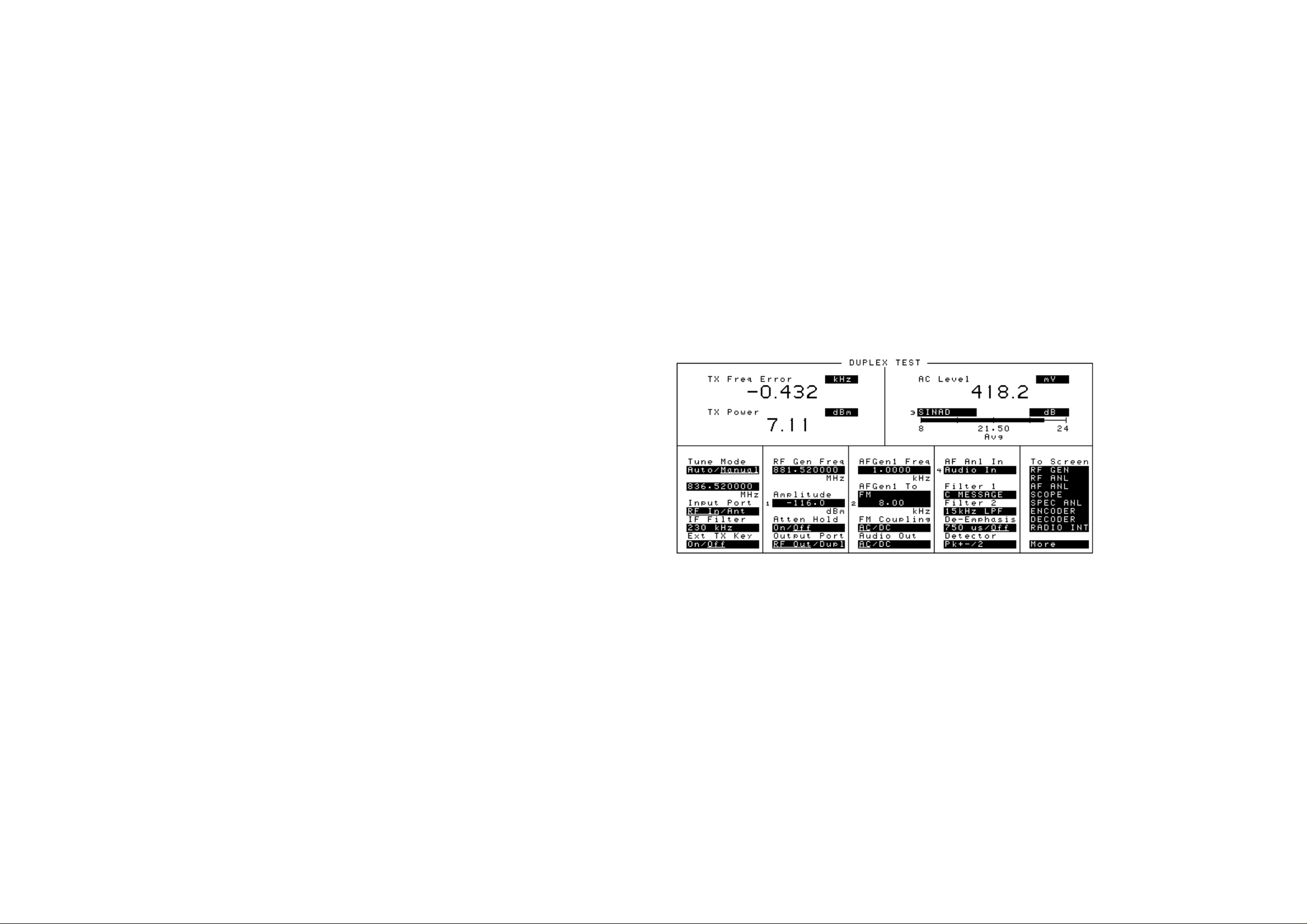
Test Analyser Set Up RX
Note these setting are for the HP 8920 on a duplex test screen.
Tune Mode – Manual AF generator 1KHz Tone - 8Khz deviation
Frequency – 836.52Mhz FM Coupling – AC
Input Port – RF IN Audio Out – AC
IF Filter – 230kHz AF Anl In – Audio In
Ext. TX Key – OFF Filter 1 CCIT or Cmessage / Filter 2 15Khz LPF
RF signal gen. to 881.52 MHz De-emphasis – OFF
Amplitude at -116dBm Atten Hold – OFF
Detector – PK+ - / 2 Output Port – RF Out
Power Meter Avg. = 10 SINAD Avg. = 10
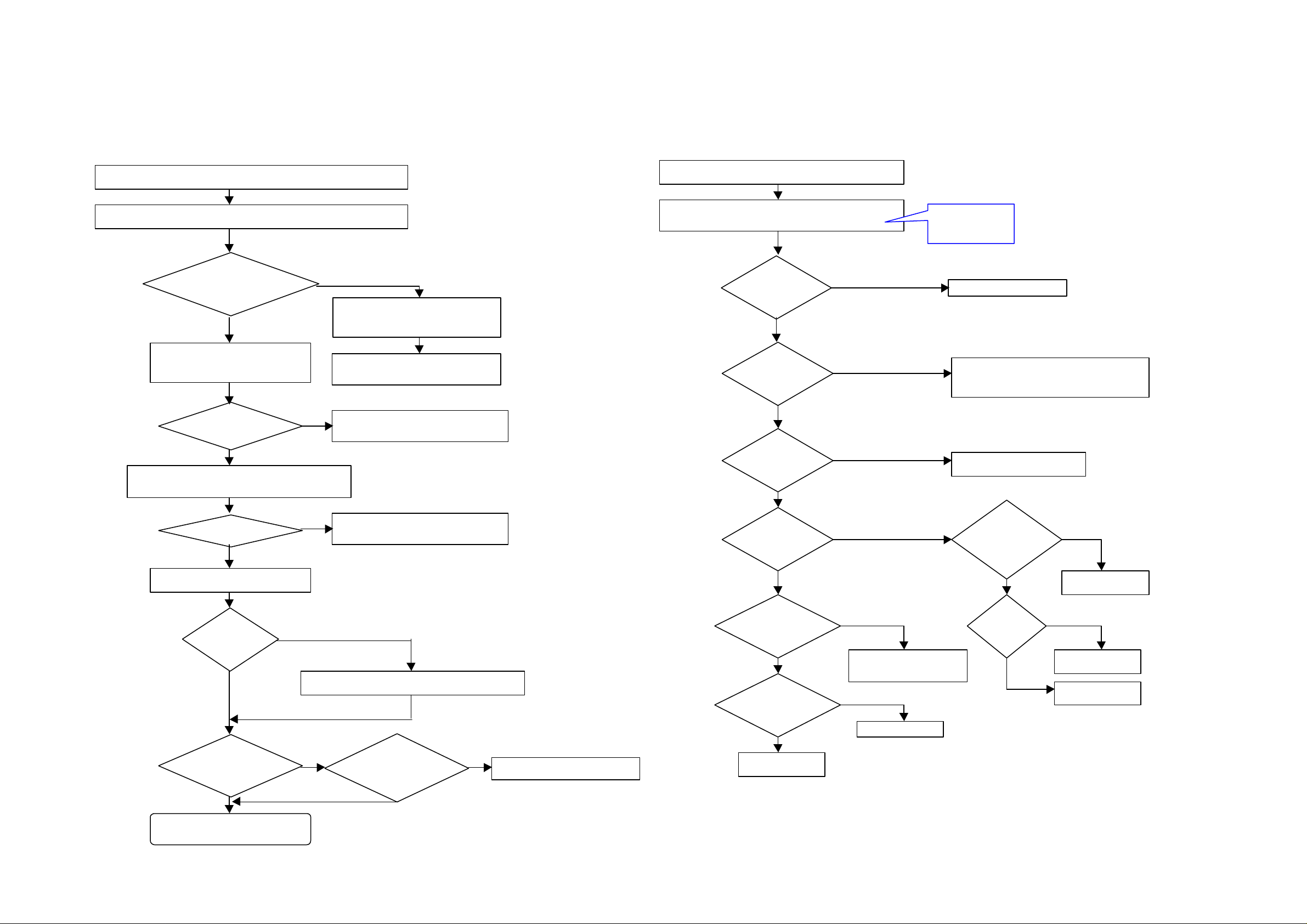
Introduction
The purpose of this section is to define module faults down to component level. The flow charts allow simple
navigation by following YES /NO routes.
Note; Some flow charts have callout boxes referring to appropriate oscilloscope readouts. If you are reading the
PDF version of this document these are hypertext links.
Required Service Equipment
NHA-9 WinTesla Service Software (product code: 8400597)
Variable Power Supply Unit
Digital Multimeter
Oscilloscope
NHA-9 Service Accessories (H700PI, 282)
MJS-7 Test Frame (PN 0775095)
When the phone is in the Module Repair JIG, the probe must be connected to the test equipment.
RS232/MBUS adapter
CMT/Marconi HP8920...
Setup the cable loss:
With the HP8920, Configure > RF level offset on/off = on > RF in/out = loss of the cable.
RF Spectrum Analyser
AAT-7 RF Probe
Issue 2 03/00 Page 1
Page 2
PAMS NHA-9
_____________________________________________________________________________________________________________________________________________________________________________________________________________
Technical Documentation Troubleshooting
Test Analyser Set Up TX
Wintesla Set Up RX
Note these setting are for the HP 8920 on a TX test screen.
Tune mode – Manual Filter 1 - Cmessage
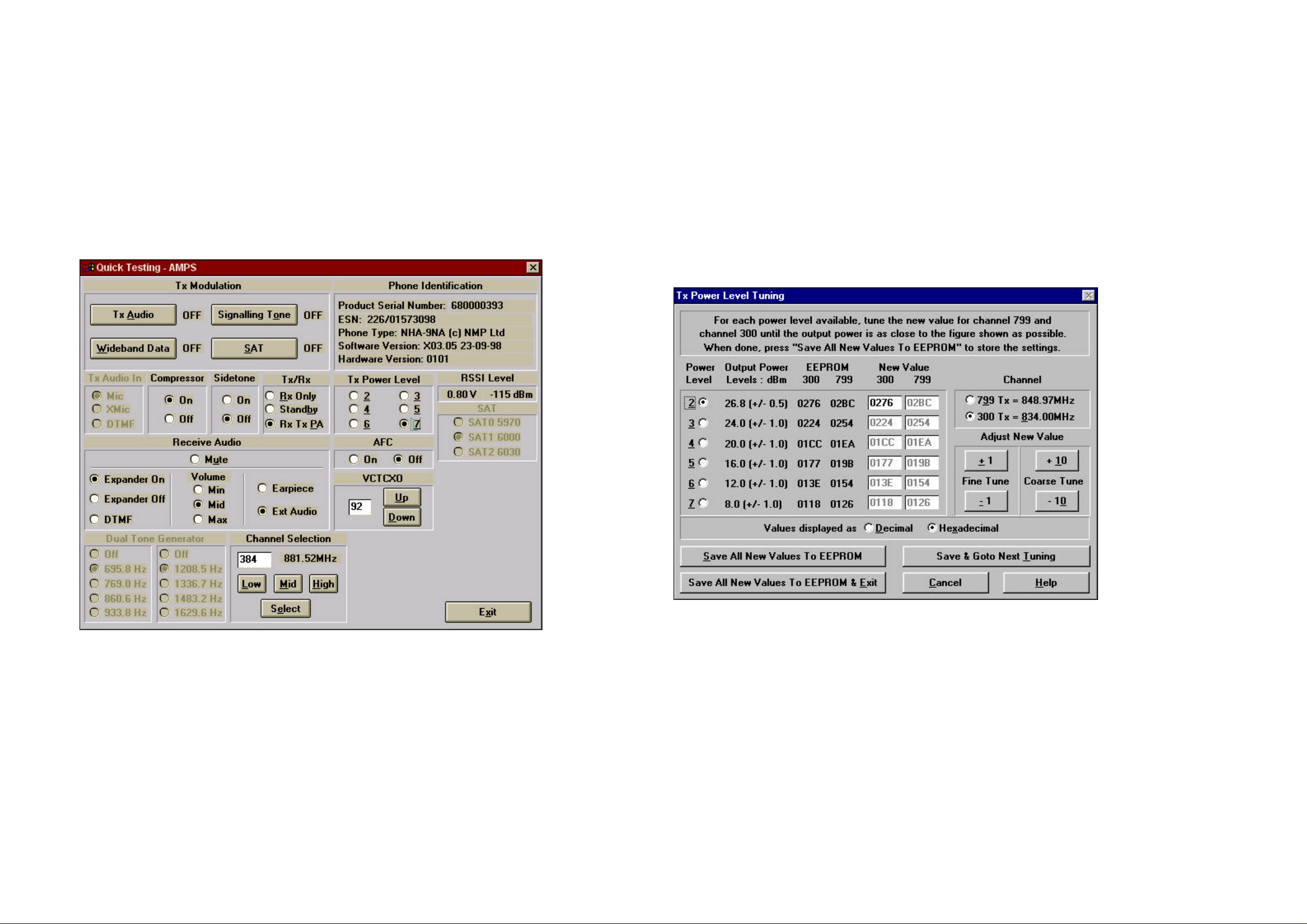
Set phone to Local mode. Go to Testing Menu enter Quick Testing.
Quicktest set up as follows:
Ex. Audio – ON Channel 384
Compressor – ON Select RX TX PA
Expander – ON Power Level 7
Volume – MID AFC – OFF
TX Frequency - 836.52Mhz Filter 2 – 15kHz
TX Pwr Meas. – Peak De-Emphasis - OFF
Input Port – RF IN Detector – PK+ - /2
IF Filter – 230kHz AF Gen. 1 – Freq. 1kHz
Ext. TX Key – OFF AF Gen. 1 – 50mV
AF Anl in – FM Demod Power Meter Avg. = 10
Wintesla Setup
Set phone to Local mode. Go to Tunings Menu enter TX Power.
Expected results with the above settings:
TX Power ≅ 26 to 27.3dBm
Expected results with the above settings:
Assembled Sinad between 14 to 50dB Nominal ≅ 19 to 30dB
In test fixture Sinad between 14 to 50dB Nominal ≅ 19 to 30dB
Issue 2 03/00 Page 2
Page 3
PAMS NHA-9
Will phone
Display / Keypad
Does display
headset
" ?
Can phone
mode?
Call setup
OK?
START
END
Perform BB7
PWRKEYX
transists
PWRKEYX transits
Check for broken PCB trace
Faulty power switch
(S2) Replace.
Correct Output
Vrx=2.8V at
Check PCB
trace for
MCUCLK short
D401 CLK falls
Replace EEPROM D402.
.
BBres goes
Replace R894 and retest.
LoBatt
Rst X
Page 4
Page 4
Check
N9/1 in =
NO
NO
RegEN goes
BattMon=
_____________________________________________________________________________________________________________________________________________________________________________________________________________
Technical Documentation Troubleshooting
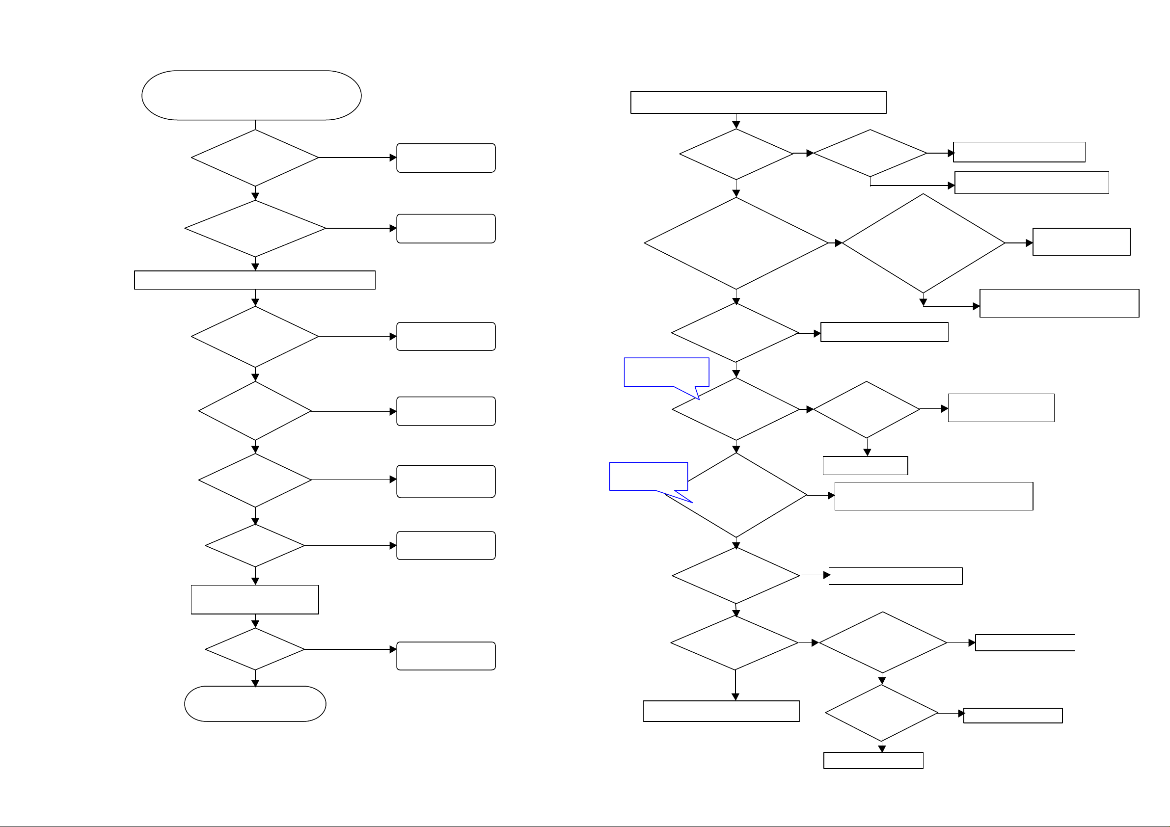
BB1 - Phone does not power up
Note: Do not dismantle phone.
power up?
operating correctly?
Insert MBUS cable with AUDIO EXT enabled on switch box.
say "Remove
NO
NO
YES
BB1
BB2
BB4b
Dismantle phone in correct fashion and place in diagnostic jig
VL=2.8 V ?
YES
NO
Check D400 and N7 pins.
See Readout
from 2.8V to 0V when
power key is pressed?
(Pin 73 of D400)
YES
high?
YES
Vbatt
from 2.8V to 0V when
power key is pressed?
(S2/3 or D400/73)
YES
Check/ replace N8 & C869
Check/ replace N9 & C839
YES
NO
between power key and D400.
enter local
RF RX OK?
RF TX OK?
(Testing TX audio.)
NO
NO
NO
NO
BB5
Rx Fault 1
(Earphone level fault.)
Tx Fault 1
BB8
See Readout
From main OSC
G1 ?
YES
burst at pin 20
D401 when power
key pressed?
NO
VBATT/2
YES
approx 2.8V
NO
NO
YES
YES
osc G1?
YES
Replace osc G1.
Retest and if still faulty replace D400
after approx
14s?
NO
shorts/open circuit.
Replace D401.
YES
NO
Issue 2 03/00 Page 3
Check R850, C405, V822 & N9.
high?
.
Replace D401.
YES
NO
Replace D400
Page 4
PAMS NHA-9
Do keys appear
Dismantle phone and place in diagnostic jig with new
Operate all keys on pad.
Replace 'A' cover
R912 &
Check for electrical shorts on C857, C858 & C859.
Replace
Replace resistors and
Return to
front page
Replace
Replace faulty component(s)
Replace 'A' cover and
Keypad
Dismantle phone and place in
Keypad
Check/ replace
Replace 'A' cover
Visible damage
Replace S1
_____________________________________________________________________________________________________________________________________________________________________________________________________________
Technical Documentation Troubleshooting
BB2 (Display / keypad not operating correctly.)
OSCOUT
Operate all keys on phone pad.
MCUCLK
and cinch
connector.
NO
and retest
YES
on display?
NO
cinch connector.
Do the numbers appear on
the display?
YES
to reed Switch
S1 ?
NO
YES
backlight
OK ?
YES
YES
NO
diagnostic jig with new cinch connector.
backlight
OK ?
NO
R869, R870,
V814, R868, V815,
R867, OK?
NO
Check / Replace D401
YES
and cinch
connector.
recheck phone.
and retest.
cinch connector.
NO
Check R912 & 922 approx 2K2 ohm.
NO
Replace Lid Module with known working unit.
YES
R922 OK?
OK?
OK?
NO
D400
OK?
YES
checks.
YES
Issue 2 03/00 Page 4
NO
D401
OK?
SCRAP.
NO
Page 5
PAMS NHA-9
Acc_ID indicates
Check headset socket in 'B'
cover
Check alignment of socket legs.
Lift cradle of jig and test outer
Check / Replace D401, R927 & R897
Visually inspect spark gaps under system
Remove spacer PCB.
Unit functions
Replace ESD device V824.
Unit still
Dismantle phone and place in diagnostic jig.
With oscilloscope, probe MBUS at system connector whilst
Scope trace
Data pulses
Data pulses
Data pulses at
R891 biasing
Check for short/foreign material at
Mbus spark
Is data line
Short on
Check PCB
trace from V812
to system connector.
R892
approx
See Readout
Check replace
_____________________________________________________________________________________________________________________________________________________________________________________________________________
Technical Documentation Troubleshooting
BB4b (Phone thinks headset accessory is inserted.)
Dismantle the phone and place engine in diagnostic jig.
Power up phone and call TESTIN>ADC READING from Wintesla.
NO
"HEADSET" ?
YES
two pins of spacer PCB.
YES
Shorted?
NO
for shorts (X359)
If in doubt, replace socket.
and retest.
BB5 (Phone cannot enter local mode.)
Power up phone.
calling VIEW>PHONE_IDENTITY from Wintesla.
10K ohm?
YES
remains low?
NO
NO
YES
Page 6
Replace R892 and retest.
gap under system connector.
Check for shorted ESD device V824.
YES
connector X360 with microscope for shorts.
Short found?
YES
NO
Recall ADC READINGS from Wintesla.
indicates
"Headset"?
YES
NO
NO
correctly?
Remove short and retest.
Check for excess solder and replace
NO
R927, C866,
R891, OK?
Replace D401 and retest.
at pin 10 of
D401?
YES
at pin 9 of
D401?
YES
R892? (One
side is VL)
NO
base of V812
correctly?
YES
Replace V812.
NO
NO
YES
NO
Replace R891.
Check R865 approx 10K ohm.
constantly
pulled high?
NO
YES
YES
V812?
NO
Replace V812
Replace D401.
Replace D401.
Return to front page checks.
Issue 2 03/00 Page 5
YES
Page 6

PAMS NHA-9
Audible 1kHz
Wintesla: menu Testing>Quick Testing - AMPS
NO
1kHz sine wave,
Dismantle phone and place in diagnostic jig
Check/replace C853 and D400
Replace lid module and
1kHz, 2.2V
YESNOYES
Check/replace
X359
1kHz, 1.4V offset,
Check/replace X360,
YESNO1kHz, 1.4V offset,
D400/44?
YES
YESNO1kHz, 1.4V offset,
C400/bottom?
YESNONO
_____________________________________________________________________________________________________________________________________________________________________________________________________________
Technical Documentation Troubleshooting
MBUS
BB6 (Earpiece or external audio fault)
1.4V offset,
1.8V pk-pk at
X358/3?
Then select: RxTxPA - ON, Tx Power Level 4,
Earpiece
HP8920: Select Rx Test screen
Then set: RF Gen Freq = 881.52MHz
AF Gen1 Freq = 1kHz
AF Gen 1 to FM at 8kHz deviation
tone in
earpiece?
Wintesla:select Ext Audio
retest
and retest.
R897
C847 R919 and C875.
Check/replace D400
Check/replace C400
offset,
1.1V pk-pk at
1.1V pk-pk at
D400/49?
0.7V pk-pk at
0.7V pk-pk at
RF fault: go to RX Fault 1
Issue 2 03/00 Page 6
Page 7

PAMS NHA-9
Sine at D400
Check system connector X360 for dry joints.
Sine at D400
Check C404.
Sine at D400
No
HP8920 reads
deviation?
Wintesla: menu Testing>Quick Testing - AMPS
Wintesla: set
Tx Audio
In -
Mic
Can taps/voice
br
Wintesla: set
Tx Audio - OFF
HP8920 reads
deviation?
Wintesla: set Signalling Tone -
HP8920 reads
deviation?
Check/replace D400
No
baseband fault found
NONOYES
YesNONO
YES
YES
Dismantle phone and place in diagnostic JIG
,
_____________________________________________________________________________________________________________________________________________________________________________________________________________
Technical Documentation Troubleshooting
BB7 (Tx audio problems)
BB7b
Then select: RxTxPA - ON, Tx Power Level - 4,
Tx Audio - ON, Tx Audio In - XMic
HP8920: Select Tx Test screen
Then set: Tune - Auto, IF Filter 230kHz
Filter 1 - 50Hz HPF, Filter 2 - 15kHz LPF, De-emp -OFF
Detector - pk+-/2, AF Gen 1 - 1kHz @ 50mV
3.9kHz
HP8920: set volume to mid
Tap or speak into mic
heard
from 8920 speaker?
set ST - ON
BB7b
BB7c
setup as per BB7 first box
side of R400?
(170mVpk-pk)
side of C404?
(170mVpk-pk)
YES
pin71?
(300mVpk-pk)
NO
Check spark gap for contaminants.
Check R400.
NO
Check PCB trace between R400 and C404.
NO
Check /Replace D400
8kHz
OFF
set SAT - ON
HP8920: set Filter 2 - 6kHz BPF
2kHz
YES
Baseband fault found, go to TXFault1
(or RF AMPS/NAMPS
selection circuits N4, Z11, Z22)
Issue 2 03/00 Page 7
Page 8

PAMS NHA-9
BB7c
Is
mic bias at 2.1V at
R409
Yes
Yes
YesNoNo
No
Power up phone.
Phone fails to
Phone fails power
Phone fails audio
Phone fails
Phone fails data
Phone fails
Check NAM programming with
Wintesla, especially SID
NAM is
Change 8920 settings
Check phone volume level is at 4.
_____________________________________________________________________________________________________________________________________________________________________________________________________________
Technical Documentation Troubleshooting
BB8 Call processing.
Connect Xear & Xmic to 8920.
Ensure phone audio level is set correctly. (4 on an 8920)
Select 'Any carrier' in phone settings.
On 8920 select TESTS, PARAMETRIC.
Select RUN TEST
X360 right hand mic
Pin?
Check R913 & D400.
Check R405 &C406
OK?
OK?
Check for shorts/damaged PCB tracks.
Replace component & retest.
Replace R409 & retest.
register?
NO
level?
NO
response?
NO
YES
YES
YES
and control channel on 8920.
correct?
YES
Consider faulty D400
Goto Txfault1.
Goto BB6 and BB7.
NO
to match phone and
re-run test.
Issue 2 03/00 Page 8
SAT/DSAT?
NO
TX/RX?
NO
compressor /
expander?
NO
Return to front page checks.
YES
YES
YES
Check headset socket and circuitry.
Replace D400 and re-run test.
Goto BB6 and BB7.
Page 9

PAMS NHA-9
1A
*Duplex
Sens.
pwr level 2 to7?
Repeat
Retest
Remove RF screen lids
OK?
Check AF @ R63
Go to earphone
ExamineN5, R51
, C105,
Increase RX signal
Open phone
,
Check LNA Boost
Inspect R59, D400
Check LO @ J12
>-14dBm?
C61 to
Check 2
nd
IF @ C75 ref.
Check p. 5 N5
Check N4, C72, Z22,
OK?
Check 14.85 ref.
Check G1 14.84MHz
Check 2
nd
LO@
-48dBm OK?
Check mixer output
Check RX freq.
Check LO
Check R44,
R55 & Z18
Check 2nd IF 450KHz
Check L6, C84 & N5 solder
joints replace if necessary
N5 solder joints replace if
No
Yes
See Readout
See Readout Page 13
See Readout
Check LNA output @
Yes
Check V10
,R47,R48,R49,R50
Replace V10 if necessary
See Readout
See Readout
See Readout
*Refer to software
* Note Due to possible differences in equipment all RF levels should be referenced to a known good product*
Technical Documentation Troubleshooting
RX Fault 1
* Measure taken with a 10:1 probe*
Receiver Fault
& equipment setup.
Test Analyzer Setup
RX & Wintesla
Setup RX.
* Simplex
Sens. RX Only
Ref. Rx fig.1&
No
Yes *yes sensitivity fail
Ref. RX Fig.
1&1A Sinad=14to
50 dBm across
Yes Yes
for High
& Low
Bands
Yes
Yes
Possible
False failure
No
No
Yes
No
inspect Ant. block
& duplexer for
replacement or
damage. OK?
A1, A5 & A6. Inspect
for dry solder joints,
missing, misplaced or
damaged components.
only Yes No
No Yes
800mVdc OK?
No
R59/ D400 p.83 ≅
&D401 for dry solder or
lifted pins. OK?
Yes No
Yes Yes
>300mV pk-pk ref.
RX fig 3
No
C99, C87, C93 & L5 for dry
solder joints, missing,
misplaced or damaged
components. OK?
level fault.
Replace D400
Page 13
See Readout Page 13
> -30dBm Ref RXfig 14
amplitude to –50dBm.Check
1st IF @ J10 ref.RX fig 2
45 MHz > -50dBm?
No
@ C90 45Mhz >
-48dBm?
ref.RX fig. 9
869.04 to 893.97MHz
@C90 >-89dBm?
ref.RXfig.10
Yes
914 to 939MHz
@C90 -60dBm?
ref.RXfig.11
914 to 939MHz
ref.RXfig4
No
Is R42 2.8Vdc?
No
See Readout Page 13
Check R44R55 &Z18
See Readout Page 13
Yes
Yes
Check C865, C82, C83, V9, L7, C96 &
Grnd ˜
1.1KO?
R52,R53,R59. C85 and C86
No
C80 ref RX fig 6 > - 60
dBm
See Readout Page 13
No
Check Z17 solder joints, V9, C83, L7, C96, & V11
Go to RX Fault 2
No No Yes
C81 44.55MHz
ref.RXfig.13
Yes No
@R46 >-30dBm
ref.RXfig.12 OK?
Yes
necessary
Page 14
Page 14
Issue 1 03/99 Page 9
C76 >-60dBm
Ref RX fig 16
Yes
Check VRX
Page 14
G2 possibly short check C64
RX fig. 5 =450KHz
>350 mv pk-pk?
Z11, C73 & C76.
If Amps R68 & R68
Yes
See Readout Page 13
Replace if necessary
Page 10

PAMS NHA-9
Transmitter Fault 1
No TX Power
TX (no or low) output
Set
pwr level 2
Measure RF level @ C23 N1's
not probe N1 pins 12&13
*
Open
phone inspect ant.
block
and solder joints for
damage.
Measure RF level @ ant.
Inspect C11, C23, C20, R3, R12, R5, R65,
Remove RF screens A1, A5
Check L2, C33, C39, C45 & R19
Check frequencies & levels @ J5
ref.
TXfig. 3
Rx Fault 2
Check J3
ref.
TXfig. 4
- 26dBm
Measure N2 p. 5
Measure gain across
Check V4p.2
>
2vd.c. If
Measure PAEN @ C9
Measure RF level
Measure RF level @
ref. TX fig.9
Check V5, C16 &
Check N1
Check DC level
Check N1
Return to & check J3 decision if coming
Check all components in the
See Readout Page 14
See Readout Page 14
* Note Due to possible differences in equipment all RF levels should be referenced to a known good product*
Technical Documentation Troubleshooting
TX Fault 1
* Measure taken with a 10:1 probe*
Put Phone into Local mode & enter the TX Power screen under
the Tunings menu
See Readout
Page 14
See Readout Page 14
high current
>650mA?
Yes
No Yes Yes No Yes Yes
duplexer for damage If OK remove RF
screen A2 & inspect all components
& A3 inspect all competent
& solder joints.
824 MHz to 849 MHz
>
No
>2.5vd.c.?
Yes Yes
No
Pwr Frequency &
Current OK?
pac to 800
Decimal output
pwr increases?
ref.TX fig.s 5&6
Yes
90MHz >-40 dBm?
ref. TX fig2
@ J12 914 to 939 MHz > -17dBm?
No
output ref TX fig.6 > 9dBm? *DO
Yes No No
No
Yes Yes
Yes
N1 >15
No No
V1 & V2. Replace Duplexer if necessary.
See Readout Page 14
90 & 900 MHz signal paths.
Replace N2 if necessary.
probe ref TX fig.10
>10dBm?
See Readout Page 14
Retest
Possible
false
Failure
p. 5 >-17dBM
ref.TX fig. 5
p. 8>2vdc?
@ p. 5 V4 >1.6vdc
No
Check R991
& D400 pin 1
See Readout Page 14
Check N1 solder joints
replace if necessary.
no check V1, R18, R3,
R7 & R 27
Yes
900 MHz OK?
No
90 MHz OK?
No
No
TX Fault 2
Issue 1 03/99 Page 10
>2.5vd.c.< 3vd.c.
Yes Yes Yes
No No No
Check C9 if ok Check
D400 & D401 solder
@ C16 > -15dBm
ref. TX fig 8
C17 OK?
Z7 output -20dBm
Check saw filter
replace if necessary
joints
Yes
from measuring N1's gain ref.TX fig.4 > 30dBm. If OK trace signal to V5.
See Readout Page 14
Check N1 Solder
Joints replace if
necessary
Page 11

PAMS NHA-9
Receiver fault 2
Check N3
Transmitter Fault 2
Measure the voltage @ N3
Check VTX @ C871
Check N3 VDD1
Measure
Is LO present @
Check loop filter C30
320kHz 3Vpk-pk @ C108
Inspect the following pins on N3 & D400 for dry solder and
Check 14.85Ref.
ref.RXfig.15
Check RF level
8
No
Set Phone to local mode enter the TX
Check loop
Yes
No
Technical Documentation Troubleshooting
RX / Tx Faults 2
Pin 18 ≅
5.2 Vd.c.
OK?
Yes
Check N3 Cntl Lines
&VDD2 ≅
2.7vd.c.
Yes
R16 = 5.6k Ω
OK?
No
No
No
* Note Due to possible differences in equipment all RF levels should be referenced to a known good product*
* Measure taken with a 10:1 probe*
Check Neg VClk line
conductivity.
SYNTHDAT N3 p.12 / D400 p.74
SYNTHCLK N3 p.11 / D400 p.73
SYNTHDATENX N3 p.13 / D400 p.76
LOCKDET N3 p.19 / D400 p.72
Check R37, R38 & Vrx
R35, C29, R16 & C32
Power Screen in the Tunings Menu
p.V17 ≅ 2Vdc?
≅ 2.8vd.c. OK?
Check
VTXEN,
replace N10 if
necessary.
yes
yes
Check C65, C63 V6, C54,
R908, C48, R70 & C43.
filter R20,R40,
C42 & C46.
Go to receiver fault 2
Repair or
replace faulty
Component
Yes
C67> -15dBm
ref. RX fig. 7
Yes
@N3p.8>-30dBm
Yes
@N3/pin 6 >
-30dBm ref RX fig
yes
See Readout Page 12
Check G2 Supply @ C61 ≅2.5Vdc
No
See Readout Page 13
Check G1
No
See Readout Page 13
No
Check C67 & C57
Replace N3
Issue 1 03/99 Page 11
Page 12

PAMS NHA-9
Technical Documentation Troubleshooting
* Note Due to possible differences in equipment all RF levels should be referenced to a known good product*
Oscilloscope Readouts
RX Fig 2:
RX Fig 2: Increase RX signal amplitude to –50dBm.Check 1st IF @ J10 , 45 MHz > -50dBm?
RX Fig 3:
* Measure taken with a 10:1 probe*
RX Fig 5:
RX Fig 5: Check 2nd IF @ C75 =450KHz >350 mv peak to peak?
RX Fig 6:
RX fig 8:
RX fig 8: Check RF level @ N3/pin 6 >-30dBm
RX Fig 9:
RX Fig 3: Check AF @ R63 >300mV peak to peak
RX Fig 4:
RX Fig 4: Check LO @ J12 914 to 939MHz >-14dBm?
RX Fig 9: Check mixer output @ C90 45Mhz >-48dBm?
RX Fig 6: Check LNA output @C80 >-60dBm?
RX Fig 10:
RX fig. 7:
RX Fig 10: Check RX freq. 869.04 to 893.97MHz @C90 >-89dBRadouts
RX fig 7: Is LO present @ C67> -15dBm
Issue 1 03/99 Page 12
Page 13

PAMS NHA-9
* Note Due to possible differences in equipment all RF levels should be referenced to a known good product*
Technical Documentation Troubleshooting
* Measure taken with a 10:1 probe*
RX Fig 11:
RX Fig 11: Check LO 914 to 939MHz @C90 >-60dBm?
RX Fig 12:
RX Fig 13:
RX Fig 13: Check 2nd LO @ C81 44.55MHz –48dBm ?
RX Fig 14:
RX fig 15
RX fig 15: Check 14.85Ref. @N3p.8> -30dBm
RX Fig 16:
RX Fig 12: Check 14.85_ref. @ R46 > -30dBm ?
RX Fig 14: Check G1 14.84MHz >-30 dBm?
RX Fig 16: Check 2nd IF 450KHz C76 > -60 dBm
Issue 1 03/99 Page 13
Page 14

PAMS NHA-9
* Note Due to possible differences in equipment all RF levels should be referenced to a known good product*
Technical Documentation Troubleshooting
TX fig2:
TX fig2: Check frequencies & levels @ J5 90MHz >-40 dBm?
TXfig. 3:
* Measure taken with a 10:1 probe*
TX fig. 5:
TX fig.9:
TX fig. 5: Check N1 p. 5 >-17dBm TX fig.s 5&6: Measure gain across N1 >15
TX fig.9: Measure RF level @ Z7 output > -20dBm
TX fig.6:
TX fig.10:
TXfig. 3: Check frequencies & levels @ J12 914 to 939 MHz >- 17dBM?
TXfig. 4:
TXfig. 4: Check J3 824 MHz to 849 MHz >- 30dBm
TXfig. 4: Return to & check J3 decision if coming from measuring N1's gain > -30dBm. If OK trace
signal to V5.
TX fig.6: Measure RF level @ C20 N1's output >10dBm? at power level 2
*DO not probe N1 pins 12&13*
TX fig 8:
TX fig 8: Measure RF level @ C16 > -15dBm
TX fig.10: Measure RF level @ ant. probe >10dBm?
Issue 1 03/99 Page 14
 Loading...