

Page 1

Programmes After Market Services
NHA–9 Series Transceivers
Chapter 3
System Module
Issue 2 03/00
Page 2

NHA–9
System Module
Technical Documentation
CONTENTS
Baseband Circuit Description 3–5. . . . . . . . . . . . . . . . . . . . . . . . . . . . . . . . . . . . . .
Internal Signals 3–5. . . . . . . . . . . . . . . . . . . . . . . . . . . . . . . . . . . . . . . . . . . . . . .
AMSA_Dig System ASIC D400 3–7. . . . . . . . . . . . . . . . . . . . . . . . . . . . . .
AMSA_Dig D400 signals 3–7. . . . . . . . . . . . . . . . . . . . . . . . . . . . . . . . . . . .
Microcontroller D401 3–8. . . . . . . . . . . . . . . . . . . . . . . . . . . . . . . . . . . . . . .
Microcontroller D401 signals 3–9. . . . . . . . . . . . . . . . . . . . . . . . . . . . . . . . .
EEPROM D401 3–10. . . . . . . . . . . . . . . . . . . . . . . . . . . . . . . . . . . . . . . . . . . .
Regulation 3–10. . . . . . . . . . . . . . . . . . . . . . . . . . . . . . . . . . . . . . . . . . . . . . . .
CHAOS2 ASIC N6 and charging control 3–10. . . . . . . . . . . . . . . . . . . . . . .
RF Circuit Description 3–11. . . . . . . . . . . . . . . . . . . . . . . . . . . . . . . . . . . . . . . . . . . . .
PAMS
Page No
Receiver 3–12. . . . . . . . . . . . . . . . . . . . . . . . . . . . . . . . . . . . . . . . . . . . . . . . . . . . .
Rx Synthesizer 3–13. . . . . . . . . . . . . . . . . . . . . . . . . . . . . . . . . . . . . . . . . . . . . . . .
Rx loop filter 3–13. . . . . . . . . . . . . . . . . . . . . . . . . . . . . . . . . . . . . . . . . . . . . . . . . .
Rx VCO 3–13. . . . . . . . . . . . . . . . . . . . . . . . . . . . . . . . . . . . . . . . . . . . . . . . . . . . . .
Tx synthesizer 3–14. . . . . . . . . . . . . . . . . . . . . . . . . . . . . . . . . . . . . . . . . . . . . . . .
Transmitter 3–14. . . . . . . . . . . . . . . . . . . . . . . . . . . . . . . . . . . . . . . . . . . . . . . . . . .
UI 3–16. . . . . . . . . . . . . . . . . . . . . . . . . . . . . . . . . . . . . . . . . . . . . . . . . . . . . . . . . . . . . .
Technical Specifications 3–16. . . . . . . . . . . . . . . . . . . . . . . . . . . . . . . . . . . . . . . .
External Signals and Connections 3–16. . . . . . . . . . . . . . . . . . . . . . . . . . . . . . .
Internal Signals 3–16. . . . . . . . . . . . . . . . . . . . . . . . . . . . . . . . . . . . . . . . . . . . . . .
Keypad Module – Version 1 3–18. . . . . . . . . . . . . . . . . . . . . . . . . . . . . . . . . . . . .
Keymat Module – Version 2 3–18. . . . . . . . . . . . . . . . . . . . . . . . . . . . . . . . . . . .
Page 3 – 2
Issue 2 03/00
Page 3

PAMS
NHA–9
Technical Documentation
System Module
List of Figures
Figure 1. Baseband Block Diagram 3–6. . . . . . . . . . . . . . . . . . . . . . . . . . . . . . . .
Figure 2. RF Block Diagram 3–11. . . . . . . . . . . . . . . . . . . . . . . . . . . . . . . . . . . . . .
Figure 3. UI Module Block Diagram 3–17. . . . . . . . . . . . . . . . . . . . . . . . . . . . . . .
Figure 4. Keypad Module Block Diagram 3–18. . . . . . . . . . . . . . . . . . . . . . . . . . .
System Diagram A–1. . . . . . . . . . . . . . . . . . . . . . . . . . . . . . . . . . . . . . . . . . . . . . . . .
PCB v2_2
Baseband Block A–2. . . . . . . . . . . . . . . . . . . . . . . . . . . . . . . . . . . . . . . . . . . . . . . . . .
CTRLU A–3. . . . . . . . . . . . . . . . . . . . . . . . . . . . . . . . . . . . . . . . . . . . . . . . . . . . . . . . .
PSU A–4. . . . . . . . . . . . . . . . . . . . . . . . . . . . . . . . . . . . . . . . . . . . . . . . . . . . . . . . . . . .
Asic A–5. . . . . . . . . . . . . . . . . . . . . . . . . . . . . . . . . . . . . . . . . . . . . . . . . . . . . . . . . . . .
RF Block A–6. . . . . . . . . . . . . . . . . . . . . . . . . . . . . . . . . . . . . . . . . . . . . . . . . . . . . . . .
Page No
TX Block A–7. . . . . . . . . . . . . . . . . . . . . . . . . . . . . . . . . . . . . . . . . . . . . . . . . . . . . . . .
RX Block A–8. . . . . . . . . . . . . . . . . . . . . . . . . . . . . . . . . . . . . . . . . . . . . . . . . . . . . . . .
AMPS Component Layout/Grid Ref. ( Bottom) A–9. . . . . . . . . . . . . . . . . . . . . . .
AMPS Component Layout/Grid Ref. ( Top) A–10. . . . . . . . . . . . . . . . . . . . . . . . . .
NAMPS Component Layout/Grid Ref. ( Bottom) A–11. . . . . . . . . . . . . . . . . . . . .
NAMPS Component Layout/Grid Ref. ( Top) A–12. . . . . . . . . . . . . . . . . . . . . . . . .
PCB v4_0
AMPS Component Layout/Grid Ref. ( Bottom) A – 13. . . . . . . . . . . . . . . . . . . . . . .
AMPS Component Layout/Grid Ref. ( Top)) A – 14. . . . . . . . . . . . . . . . . . . . . . . . .
Note: Positional changes in AMPS only, for schematics refer to version 2_2
PCB v11_1
Baseband Block A –15. . . . . . . . . . . . . . . . . . . . . . . . . . . . . . . . . . . . . . . . . . . . . . . . . .
CTRLU A –16. . . . . . . . . . . . . . . . . . . . . . . . . . . . . . . . . . . . . . . . . . . . . . . . . . . . . . . . .
PSU A –17. . . . . . . . . . . . . . . . . . . . . . . . . . . . . . . . . . . . . . . . . . . . . . . . . . . . . . . . . . . .
ASIC A –18. . . . . . . . . . . . . . . . . . . . . . . . . . . . . . . . . . . . . . . . . . . . . . . . . . . . . . . . . . .
RF A –19. . . . . . . . . . . . . . . . . . . . . . . . . . . . . . . . . . . . . . . . . . . . . . . . . . . . . . . . . . . . .
TX A –20. . . . . . . . . . . . . . . . . . . . . . . . . . . . . . . . . . . . . . . . . . . . . . . . . . . . . . . . . . . . .
RX A –21. . . . . . . . . . . . . . . . . . . . . . . . . . . . . . . . . . . . . . . . . . . . . . . . . . . . . . . . . . . . .
AMPS Component Layout (Bottom) A –22. . . . . . . . . . . . . . . . . . . . . . . . . . . . . . . . .
AMPS Component Layout (Top) A –23. . . . . . . . . . . . . . . . . . . . . . . . . . . . . . . . . . . .
NAMPS Component Layout (Bottom) A –24. . . . . . . . . . . . . . . . . . . . . . . . . . . . . . .
NAMPS Component Layout (Top) A –25. . . . . . . . . . . . . . . . . . . . . . . . . . . . . . . . . .
Note: In printed manuals all A3 drawings are located at the back of the binder
Issue 2 03/00
Page 3 – 3
Page 4

NHA–9
System Module
PAMS
Technical Documentation
[This page intentionally left blank]
Page 3 – 4
Issue 2 03/00
Page 5

PAMS
NHA–9
Technical Documentation
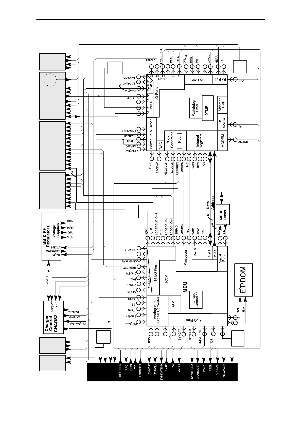
Baseband Circuit Description
The audio/logic unit consists of 4 ICs: AMSA_Dig baseband system ASIC
D400, MCU D401, EEPROM D402, and CHAOS2 charger switch ASIC
N6. These ICs together with the supporting discrete circuitry make up the
Baseband block.
Internal Signals
Table 1. Baseband / RF interface signals
Control signal Description
VBATT Battery supply voltage
GND Battery ground connection
PAC Filtered PWM power control signal for the transmitter
PAEN Power amplifier enable
VTX Regulated dc voltage for the low power transmitter stages
TXI Indicates when RF is present at the output of the transmitter
System Module
SynthENX Enables extended standby mode
VRX Regulated dc voltage for the receiver
FSEL Selects AMPS/NAMPS 2nd IF filtering
RSSI Received signal strength indication
RXAF Received audio and data
IF2 2nd IF providing input to the AFC loop
LNABOOST Linearises the LNA in transmit mode
SYNDATENX Serial data enable for the synthesiser
SYNDAT Serial data bus for programming the synthesiser
SYNCLK Serial data clock input for the synthesiser
LNAENX Enables the power supply to the LNA used in High signal areas
AFCDAC Voltage used to control TCXO output frequency
LOCKDET Indicates when synthesisers are in lock
TXMOD Modulation signal containing AMPS/NAMPS modulation
REFFREQ VCTCXO output used to provide baseband clock
NEGVCLK 320KHz clock for phase detector voltage doubler
Issue 2 03/00
Page 3 – 5
Page 6
NHA–9
System Module
PAMS
Technical Documentation
Socket
Headset
Mic
Element
System ConnectorUI ConnectorKeypad
GND
XMic
HEAR
HSET_DET
Mic
GND
CHGRGND
Acc_ID
XMic
HEAR
VCH
ChrgCtrl
MBUS
VBB
LCDENX
LCDRstX
LCDCLK
LCDSDCLK_Col3
LCDSDA_Col1
LCDDC_Col0
BuzzPWM
IntEarEn
EARP
GND
VBATT
Light0
Row(0:4)
LCDSDCLK_Col3
Col2
LCDSDA_Col1
LCDDC_Col0
GND
VBATT
FNLIGHT
NUMLIGHT
Flip
position
detect
HSET_DET
LNAENX
T6
AMSA_Dig
HEAR
Filter
Audio
Button
Baseband Block Diagram
CHGRGND
I_Sense
GND
BSI
Battery
Contacts
Vibra
Contacts
VBATT
VIBRA
VBATT
RF
Vibra
VRX
Driver
VTX
LED
Drivers
Keypad
driver
indicator
Button
I_Sense
GND
VBATT
Call–alert
LNAENX
Page 3 – 6
Figure 1. Baseband Block Diagram
Issue 2 03/00
Page 7

PAMS
NHA–9
Technical Documentation
AMSA_Dig System ASIC D400
AMSA_Dig is a 100pin TQFP mixed signal ASIC with the following
functionality:
– Power–on / reset control, watchdog timer.
– Modem for AMPS/NAMPS
– Audio Processing for AMPS/NAMPS
– PLL and clock generation for BB system (using VTXCO as reference)
– I/O ports, allowing interrupt controlled MCU activity from keyboard and
accessories.
AMSA_Dig D400 signals
pin
Power up / Reset /Clock generation signals
2 LoBattRstX Low battery reset input
3 OnRstX PLL–on reset delay input.
73 PwrKeyX Power key input for power on only
74 ChrgDet Charger detection input for power on only.
76 RegEn VRX regulator and MCU enable.
20 MCUClk 4.8MHz MCU clock output
98 BBRstX MCU reset
4 NegVClk 320kHz clock for RF voltage doubler.
5 LCDClk 160kHz LCD clock output
93 PLLRC PLLRC filter connection for the 14.8MHz AMSA_Dig PLL.
95 TCXO External 14.85MHz reference input for AMSA_Dig PLL
AMSA / MCU interface
22 – 29 D7 – D0 Data bus
31 – 36 A0 – A5 AMSA_Dig Address bus
37 RdX AMSA_Dig read enable
38 WrX AMSA_Dig write enable
40 CS AMSA_Dig chip select
41 IntX MCU interrupt output
RF control signals
53 AFCDAC DAC output controlling VTCXO frequency
89 IF 450kHz 2nd IF counter input.
86 LNAENX LNA power enable .
81 FMEN PLL PM modulation enable, for blocked channel elimination.
83 LNABOOST Open drain linearises the LNA in transmit mode
84 VTXEN VTX enable signal
85 FSEL AMPS/NAMPS filter selection
87 PAEN Transmit PA enable signal
97 SynthENX Extended standbymode enable
UI / accessory control signals
label Function
System Module
Issue 2 03/00
Page 3 – 7
Page 8

NHA–9
System Module
pin Functionlabel
7 ACC_ID Accessory detection
8 ButtDet Headset button detection
9 HSET_DET Headset presence detection
10 FLIP_DET Flip position detection
13 LCDRstX LCD reset signal
14 –18 Row (4:0) Keyboard Row0 to Row 4
Receive path signals
43 VRef DC bias for RX path. Decoupled to GND
49 HDSet Accessory external audio output (HEAR signal)
46 EARP Internal earpiece audio output
Transmit path signals
58 XMic Accessory microphone audio input
59 BMic2 Internal microphone dc bias voltage.
60 BMic1 Headset dc bias / handsfree mute voltage.
61 CMic decoupling pin for BMiC
63 Mic2 Internal microphone audio input.
64 Mic1 Headset microphone audio input.
65, 68 MicGain 1 , 2 Mic amplifier gain feedback path
71 TxO Transmit modulation audio output to RF
82 BMicDis Discharge for BMic2 capacitor.
PAMS
Technical Documentation
Microcontroller D401
This 80pin TQFP MCU has the following features: internal ROM with code
protection, RAM, 8 channel 10bit A–D converter, Serial interface, and 6
configurable I/0 ports.
Page 3 – 8
Issue 2 03/00
Page 9

PAMS
NHA–9
Technical Documentation
Microcontroller D401 signals
pin
1 PAC TX power control
3 BuzzPWM Buzzer signal to UI PCB
4 TXI Transmit detection
7 ChrgMonPull ChrgMon adjustment (high Z in reset, logic 0 when MCU running.)
9 TxD MBUS transmit serial data
10 RxD MBUS receive serial data
13 – 20 D0 – D7 AMSA_Dig data bus
22 – 27 A0 – A5 AMSA_Dig address bus
31 Col0 Keypad–Matrix Column 0
32 Col1 Keypad–Matrix Column 1
33 Col2 Keypad–Matrix Column 2
34 Col3 Keypad–Matrix Column 3
35, 36 Light0, Light1 Backlighting control
37 IntEarEn Internal earpiece driver enable
38 CallAlert Call alert LED enable
39 RdX AMSA_Dig read control line
40 WrX AMSA_Dig write control line
41 CS AMSA_Dig chip select
59 I_SENSE Charging current sense
60 RSSI Signal strength indication
61 Button Headset button detection
62 Temp Phone temperature
63 BSI Battery size indication
64 ACC_ID Accessory identification
65 ChrgMon Charger voltage monitor
66 BattMon Battery voltage monitor
70 IntX AMSA_Dig interrupt
72 LOCKDET Synth lock detect
73 SYNCLK Synth Control, clock
74 SYNDAT Synth Control, data
75 ChrgCrtl ELVI fast charger control (32Hz)
76 SYNDATENX Synth Control, enable
77 VIBRA Vibration alert enable
78 SDA I2C Bus, data,
79 ChrgSW Charger switch control for Chaos2
80 SCL I2C Bus, clock
label Function
LCDDC Serial LCD driver data or command.
LCDSDA Serial LCD driver data
LCDSDCLK Serial LCD driver data clock
System Module
Issue 2 03/00
Page 3 – 9
Page 10

NHA–9
System Module
EEPROM D402
This memory device contains non–volatile memory used to store user
defined memory locations, subscriber information, phone tuning data, and
production and service data. ESN is stored in protected one time
programmable section. Bi–directional communication is by serial I
to the MCU.
Regulation
There are 3 regulators producing the baseband and RF supplies. The
nominal voltage is 2.8V±14mV for each regulator:
– Baseband regulator, N8, is the baseband supply from which VL, VA,
VPLL,and VBB is derived.
N8 is enabled by voltage detector N9, when VBATT is of a sufficient
voltage to guarantee a valid baseband supply. If VBATT falls below the
detector threshold, N9 will turn off the baseband supply and put the
phone into reset.
PAMS
Technical Documentation
2
C bus
– VRX regulator, N7, is the supply for the RF receive section.
It is enabled by RegEn signal from the AMSA_Dig power up block.
– VTX regulator , N10 is the supply for the parts of the Tx that require a
regulated voltage. It is enabled by the VTXEN signal from AMSA_Dig
whenever the Tx path is required.
CHAOS2 ASIC N6 and charging control
CHAOS2 is basically an analog switch controlled by software, with some
additional integrated protection and start–up mechanisms.
When a charger is connected, CHAOS2 provides a start–up current of
60mA (nom) to VBATT, up to 4.0V(max). When SW recognises the
charger via ChrgMon A–D input on the MCU, it takes over control of the
charger current flow to the battery by controlling Chaos2 with ChrgSW
signal.
ChrgMon has two ranges controlled by open drain ChrgMonAdj signal:
ChrgMonAdj=0 is the default. ChrgMonAdj = open is only used when
sensing current across CHAOS2 when using the 3 wire ELVI fast
chargers.
When phone is in reset, ChrgMonPull is high impedance to ensure there is
sufficient voltage on ChrgMon at AMSA_Dig pin74 to wake up the phone.
Page 3 – 10
Issue 2 03/00
Page 11

PAMS
NHA–9
Technical Documentation
RF Circuit Description
824 – 849 MHz
TXDUPI
Power
coupler
TXPAO
Power
Control
PA
TXPAI
Tx Filter
TXDUPO
4–pole
Duplexer
4–pole
4–pole
PTXANT
869 – 894 MHz
PRXLO
LPF
LNA
Interstage
Filter
Rx Mixer
System Module
LNA Boost
SAW
VRX
SynthENX
LNAENX
VR_SW
IF AMP
PAEN
GND
90MHz
VHF VCO
VBATT
VTX
TXIF
Loop Filter
PAC
TXBO
824 – 849 MHz
TXMO
TXLO
Tx Mixer
Tx & Rx Synthesizer
TXI
NEGVCLOCK
TXMOD
SYNCLK
SYNDATENX
LOCKDET
VRXSYN
SYNDAT
REFFREQ
914 – 939MHz
UHF VCO
VTCXO
14.85MHz
AFCDAC
VRXVCO
44.55MHz
X3
RSSI
450KHz
FM IF Processor
RXAF
IF2
First IF Filter 45MHz
AMPS NAMPS
FSEL
RTEMP
VRX
RXENX
LNABOOST
Issue 2 03/00
Figure 2. RF Block Diagram
Page 3 – 11
Page 12

NHA–9
System Module
Receiver
The receiver is a dual–conversion super–heterodyne using two
intermediate frequencies, 45 MHz and 450 kHz. The design implements
the necessary filtering and control required for NAMPS operation although
these components will not be fitted in AMPS only modules.
The RF signal from the duplexer RX port (via an additional low pass filter)
is applied to the RF amplifier. The amplifier is realized with transistor V10.
Amplifier stage input matching is accomplished with Z20 and Z23. R49,
R53, R47 and R52 are used for biasing. Output matching is carried out by
Z13 and Z14, R48 provides wideband stability. Components C86, and C85
are used for RF bypassing.
There is additional circuitry, R59 and C91, to boost the LNA current in Tx
mode.
V10 (LNA transistor) is switched off in high signal conditions to improve
the IMD performance of the receiver. This is done via V14.
PAMS
Technical Documentation
Next the signal is filtered with Z17. The filter is followed by a single
balanced diode mixer, realized with a printed balun, C82, C83 and V9.
C82 is a precise tolerance capacitor.
After the mixer the 45MHz IF signal is amplified with V11. The input
matching is realized with L7, C96, C102 and L9 which also forms a
22.5MHz notch. The purpose of this notch is to effectively improve the
IIP2 performance of the amplifier with respect to the half IF. The output
matching is formed by L8, R44, C90 and C89.
After the IF amplifier the 45 MHz IF signal is filtered with crystal filter Z18.
Output matching is provided by R55 and dc is blocked by C94.
The second mixer, the LO buffer transistor, IF amplifier and quadrature
detector are all integrated in the circuit N5. The second LO frequency,
44.55 MHz, is the third harmonic of the VCTXO frequency. The LO signal
is realized with tank circuit C81, C84 and L6. After the mixer the 450kHz
IF signal is filtered with ceramic filters Z22 (NAMPS) or Z11
(AMPS/NAMPS). Selection is made using an integrated switch N4. The IF
amplifier output signal is phase shifted by resonance circuit C99, C87,
R51 and L5. After this the signal is fed to a quadrature detector, this
multiplies the phase shifted signal with the original limited 450KHz IF.
The output of the limited 450KHz IF is buffered using V12 and associated
components. This is used for AFC.
The signal RXAF is low pass filtered by R63 and C106. The RXAF, RSSI
and IF2 signal (450 kHz) are fed to the AMSA_Dig ASIC.
Page 3 – 12
Issue 2 03/00
Page 13

PAMS
NHA–9
Technical Documentation
Rx Synthesizer
The UHF LO signal is generated by a digital phase locked loop (PLL). The
output frequency of the loop is obtained from a voltage–controlled
oscillator (VCO). The loop gain, and hence the bandwidth, of the PLL
can be varied by data word programming. The VCO output signal is
sufficiently high to drive the receiver mixer. The injection level required by
the receiver mixer is about +2 dBm. In addition, the signal from the VCO is
fed to the synthesizer input and the transmit mixer LO port.
The overall division ratio of the chain is selected within the synthesizer
according to the desired channel.
The internal dividers of the dual synthesizer are programmed serially on
the SYNDAT (synthesizer data) line from the processor into an internal
shift register also located in the synthesizer. Data transfer is timed with
SYNCLK clock pulses.
The divided frequency is compared with a highly stable reference
frequency by a phase comparator in the PLL circuit. The phase
comparator controls the VCO frequency by means of a DC voltage
through the loop filter so as to keep the divided frequency applied to the
phase comparator equal to the fixed reference frequency.
The reference frequency is 10 kHz for both transmit and receive synthesizers. This reference frequency is obtained from voltage controlled crystal oscillator (VCXO). Oscillator frequency is 14.85 MHz. The VCXO frequency is divided by 1485.
System Module
Rx loop filter
The phase comparator output is pin 3. If the VCO frequency is too high,
the output goes low and discharges the integrator capacitor C30. After
this, the DC control voltage and the VCO frequency will decrease.
If the VCO frequency is too low, the output goes high and charges the
integrator capacitor C30. Thereafter the DC control voltage and the VCO
frequency will go up.
Output pulses from the phase detector have to be supplied to the loop
filter. The function of the integrator is to convert positive and negative
pulses to a steady DC voltage. The remaining ripple and AC components
are filtered in the lowpass filter.
Rx VCO
The VCO (circuit ref. G2) produces a level of +2 dBm level to the first Rx
mixer and delivers about –10dBm to both the synthesiser and the Tx
mixer.
Issue 2 03/00
Page 3 – 13
Page 14

NHA–9
System Module
Tx synthesizer
The transmitter synthesizer generates a frequency modulated 90 MHz
fixed frequency signal for the transmitter section. The final output
frequency is generated by mixing the Rx LO with 90 MHz and extracting
the lower sideband.
The TX offset synthesizer consists of a 90 MHz PLL circuit, passive loop
filter and a 90 MHz VCO equipped with a chip coil resonator. The
bandwidth of the PLL can be varied by data word programming.
Modulation is brought to the VCO and applied to the opposite end of the
varactor.
See later for description of modulation filters.
TX VCO
The VCO is a Clapp type oscillator. The oscillator ’s resonance frequency
is determined by a standard parallel LC tank circuit. The centre frequency
of the resonance circuit is adjustable only by use of the PLL and contains
no alignment. The VCO signal is fed directly to the prescaler and to the Tx
mixer.
PAMS
Technical Documentation
Tx loop filter
Output current pulses from the phase detector are supplied to the loop
filter. These are then integrated, which converts positive and negative
current pulses to a DC voltage. The remaining ripple is filtered in the
low–pass filter accomplished with resistors and capacitors.
TX Data Filter
For the AMPS phones this filter is a potential divider circuit made up of
R30 , R26 and R29. This enables the correct deviation to be set by AMSA
DIG.
For NAMPS this filter is more elaborate and gives pre distortion of the
modulation data at 8HZ to prevent the 90MHz PLL from tracking the
modulation signal. This filter consists of R78 , R76 , R77 , R31 and C28.
Transmitter
The modulated signal from the transmit mixer is applied to the input of
the transmit mixer buffer. This stage requires high gain and linearity, it’s
function is to amplify the transmit signal up to the required drive level for
the power amplifier.
The buffer must have good linearity to prevent the generation of
intermodulation products. The input of the amplifier is matched to the
mixer output impedance with the output of the amplifier directly matched
to 50 Ohms. The buffer is switched ON with the power amplifier enable
control signal.
Page 3 – 14
Issue 2 03/00
Page 15

PAMS
NHA–9
Technical Documentation
The output of the transmit mixer buffer then passes through a SAW filter .
The filter is used to reduce the level of unwanted spurii and transmitter
noise due to the Tx mixer buffer, mixer and oscillator circuits. The output
of the filter drives directly into the PA MMIC.
The power amplifier is an integrated 2 stage RF gain block using GaAs
technology. The device is capable of +31.5dBm output power at 3.6V with
a minimum of 50% efficiency. Output power control is achieved by varying
the voltage on the VPC input. Internally VPC sets the bias to both stages
in the MMIC. There is no negative voltage required with this device.
ALC is used to maintain the power output over frequency, temperature
and battery voltage variation. The RF is detected via directional coupler
and Schottky diode. Rectified RF is compared with a filtered PWM
reference from baseband. This provides an error signal used to control a
series PNP transistor connected between VBATT and VPC.
The PWM signal must be filtered to prevent the generation of AM
sidebands. This filtering must be sufficient to reduce the sidebands and
also meet the power level switching time specification.
System Module
A TXI signal is used to prevent false transmissions. This signal is
monitored by the microprocessor and if the level is not appropriate for the
status of the transmitter, the PA is disabled.
AFC function
The transceiver unit is equipped with AFC function, i.e. it uses the
incoming receive signal from base station as a frequency reference. The
control loop consists of the receiver, the IF counter and an 8–bit D/A
converter in the AMSA_Dig ASIC and the VTCXO, which is used as a
reference oscillator of the synthesizer.
The 2nd IF signal (450 kHz) from the receiver is fed to AMSA_Dig. The IF
counter counts the received frequency. If the frequency differs from the
programmed value, the CPU adjusts the frequency of the VTCXO by
changing the output voltage of the D/A converter. This adjustment
continues until the desired receive frequency is achieved. AFC is not
active during a channel scan.
Note: In printed manuals all A3 drawings are located at the back of the binder
Issue 2 03/00
Page 3 – 15
Page 16

NHA–9
System Module
UI
This document contains the shortform technical description of the modules
which comprise the user interface of H700–Pi. These are the lid module
(PU4C) and the keypad module (9794012) / keymat module (9794031)
The H700–Pi lid module contains:
– the buzzer and drive circuit,
– the earpiece and drive circuit,
– the LCD and drive circuit,
– the LCD backlight LEDs and their drive circuit,
– the flip detect magnet.
Technical Specifications
PAMS
Technical Documentation
Modes of Operation
Not applicable. There is no mode control on the lid and keyboard
modules, they are under system module control.
External Signals and Connections
The lid module has one external connection to the system module via an
FPC ’tail’ to an 18–way connector mounted on the system module.
The keypad module has one external connection to the system module via
a 13–way ’Cinch’ connector retained in the mechanics.
Internal Signals
Not applicable.
Lid Module Functional Description
The dynamic earpiece (B1) is driven by an audio power amplifier (N1) with
a differential output. The driver can be disabled by a shutdown signal from
the system module inverted by transistor V3. The earpiece is retained in
the LCD lightguide and connected to the FPC by a pair of spring contacts.
The buzzer (B2) is driven from a two stage buffer formed by transistors V3
and V13 and associated components. The buffer is supplied with a PWM
waveform from the system module. The frequency varies the tone and the
duty cycle acts as a crude volume control, maximum volume being
achieved at 50% duty.
Page 3 – 16
Issue 2 03/00
Page 17

PAMS
NHA–9
Technical Documentation
The LCD (H1) has its own integrated driver chip mounted on the tab which
is bonded to the LCD glass. The tab is bar–soldered onto the main UI
FPC. The driver has an on–chip voltage tripler which has two external
reservoir caps (C26 & C27). The voltage tripler output is decoupled via
C25 and supplies the contrast control circuit. The V5 input can be varied
in 32 steps to vary the contrast. The divider R25/R26, decoupled by C23,
provides the reference for the contrast control. The individual bias levels
for pixel driving have external decoupling (C19–C22). The driver is
controlled via an I
plus RAM for up to 4 programmable characters.
The LCD backlights are 6 LEDs (V6–V11), driven by a current source (V12
and associated components) which is controlled by a signal from the
system module.
The flip detect magnet operates a reed switch on the engine board to
signal whether the lid is open or shut.
System Module
2
C–type bus and contains its own character set in ROM
EarP
IntEarEn
BuzzPWM
LCDCLK
LCDRstX
LCDSDCLK_Col3
LCDSDA_Col1
LCDENX
LCDDC_Col0
Light1
VBB
VBATT
GND
ESD_GND
UI
Connector
VBATT
GND
VBATT
GND
VBATT
GND
Earpiece
Driver
Buzzer
Driver
VBB
GND
LCD Backlights
& Driver
LCD Driver
Support
Components
Earpiece
Buzzer
&
25
Figure 3. Lid Module Block Diagram
LCD
Issue 2 03/00
Page 3 – 17
Page 18

NHA–9
System Module
Keypad Module (version 1)
The keypad module contains an FPC covered with a self–adhesive tape
carrying an array of 20 metal domes. Each dome are positioned over two
concentric rings and depressing the dome makes contact between a row
and a column line indicating which key is pressed.
The 12 backlight LEDs are also mounted on the FPC, 6 light the function
keys and 6 the numeric keys. The current source drivers are located on
the system module for reasons of skyline.
PAMS
Technical Documentation
LCDSDCLK_Col3
Col2
LCDSDA_Col1
LCDDC_Col0
Row(4:0)
GND
NUMLIGHT
VBATT
FNLIGHT
Keypad
Connector
5
Figure 4. Keypad Module Block Diagram
Keymat Module (version 2)
The keypad consists of an array of 20 metal domes each dome being
positioned over two concentric rings. Depressing the dome makes contact
between a row and a column line indicating which key is pressed.
Keypad
Switch
Matrix
Number Key
Backlight LEDs
Function Key
Backlight LEDs
The 12 backlight LEDs are also mounted on the engine PCB, 6 light the
function keys and 6 the numeric keys. The current source drivers are
located on the system module for reasons of skyline.
Page 3 – 18
Issue 2 03/00
 Loading...