

Page 1

Nokia Customer Care
RH-53/54
8-System Module
ISSUE 1 09/2004 Copyright © 2004 Nokia Corporation. All Rights Reserved.
Page 2

RH-53/54
Nokia Customer Care 8-System Module
[This page left intentionally blank]
2 COMPANY CONFIDENTIAL ISSUE 1 09/2004
Copyright © 2004 Nokia. All Rights Reserved.
Page 3

RH-53/54
8-System Module Nokia Customer Care
Table of Contents
Page No
Abbreviations ......................................................................................................6
Introduction ......................................................................................................... 9
Technical Summary........................................................................................... 9
List of Features................................................................................................ 10
Technical Specifications ..................................................................................12
Modes of Operation ......................................................................................... 12
No supply .......................................................................................................12
Power off ........................................................................................................12
Acting dead ....................................................................................................13
Active .............................................................................................................13
Sleep mode ....................................................................................................13
Charging ........................................................................................................13
Regulators........................................................................................................ 14
DC Characteristics........................................................................................... 15
Supply Voltage Ranges .................................................................................15
Regulators Voltage Ranges ...........................................................................16
Interconnection Diagram.................................................................................. 17
External Signals and Connections................................................................... 17
Battery connector ...........................................................................................17
Baseband - RF interface ................................................................................18
Internal Signals and Connections.................................................................... 18
Audio ..............................................................................................................18
Speaker (Ringer & Earpiece) ......................................................................... 19
Hinge flex connection .....................................................................................19
Baseband board clocks.................................................................................... 21
Functional Description .....................................................................................22
Audio External ................................................................................................22
Headset Detection .........................................................................................22
PnPHF Detection ...........................................................................................23
Audio Internal................................................................................................... 23
Earpiece/Ringer .............................................................................................23
Microphone ....................................................................................................24
Vibra................................................................................................................. 25
Introduction ....................................................................................................25
Acoustic design ..............................................................................................25
Batteries........................................................................................................... 25
Keyboard.......................................................................................................... 26
Display & Keyboard Backlight.......................................................................... 27
LCD Backlight ................................................................................................27
Keyboard light effects ....................................................................................27
LCD.................................................................................................................. 28
ISSUE 1 09/2004 COMPANY CONFIDENTIAL 3
Copyright © 2004 Nokia. All Rights Reserved.
Page 4

RH-53/54
Nokia Customer Care 8-System Module
Memory Module............................................................................................... 28
Fold detection-switch....................................................................................... 28
SIM Interface.................................................................................................... 28
SIM -reader ....................................................................................................29
SIM switch and card detection ....................................................................... 29
Assembly ...........................................................................................................31
Flex.................................................................................................................. 31
Security.............................................................................................................. 32
Test Interfaces................................................................................................... 33
Connections to Baseband................................................................................ 33
FBUS Interface ................................................................................................ 34
Test points ....................................................................................................... 34
RF Functional Descriptions ............................................................................. 36
RF block diagram............................................................................................. 36
Frequency synthesizers................................................................................... 36
VCXO .............................................................................................................36
VCO ...............................................................................................................36
PLL Synthesizer, Functional Description .......................................................37
Receiver........................................................................................................... 37
AGC ...............................................................................................................38
Transmitter....................................................................................................... 38
Dual band FEM ..............................................................................................38
Power control scheme ................................................................................... 38
List of Figures
Page No
Fig 1 RH-53/54 bb block diagram ......................................................................... 9
Fig 2 IPower distribution diagram.......................................................................... 17
Fig 3 Flex con. pin out........................................................................................... 20
Fig 4 External audio interface ............................................................................... 22
Fig 5 Earpiece/ringer interface..............................................................................24
Fig 6 Microphone interface.................................................................................... 25
Fig 7 BL-4C battery............................................................................................... 26
Fig 8 Keyboard PWB layout.................................................................................. 26
Fig 9 UEM, UPP and SIM interface....................................................................... 28
Fig 10 Upper block B-cover SIM-slide slot............................................................ 29
Fig 11 SIM draw and switch.................................................................................. 30
Fig 12 Test pattern............................................................................................... 33
Fig 13 RF block diagram....................................................................................... 36
Fig 14 Simplified BB, either I or Q channel ...........................................................37
Fig 15 Power loop.................................................................................................38
4 COMPANY CONFIDENTIAL ISSUE 1 09/2004
Copyright © 2004 Nokia. All Rights Reserved.
Page 5

RH-53/54
8-System Module Nokia Customer Care
[This page left intentionally blank]
ISSUE 1 09/2004 COMPANY CONFIDENTIAL 5
Copyright © 2004 Nokia. All Rights Reserved.
Page 6
RH-53/54
Nokia Customer Care 8-System Module
Abbreviations
Abbr. Description
ADC Analog Digital Connector
ASIC Application Specific Integrated Circuit
ATR Answer To Reset
BB Baseband
BL-4C Battery type.
BSI Battery Size Indicator
Cbus Control bus (internal phone interface between UPP-UEM)
CTSI Clock Timing Sleep and Interrupt
Dbus DSP controlled bus (Internal phone interface between UPP-UEM)
DC Direct Current
DCT4.0 Digital Core Technology, generation 4.0
DSP Digital Signal Processor
EMC Electro Magnetic Compatibility
ESD Electro Static Discharge
Fbus Fast Bus, asynchronous message bus connected to DSP (communications
bus)
FPC Flexible printed circuit
GENIO General Purpose Input/Output
GPRS General Packed Radio Services
HW Hardware
IF Interface
IMEI International Mobile Equipment Identity
LCD Liquid Crystal Display
LDO Low Drop Out
LED Light Emitting Diode
Li-Ion Lithium Ion battery
Lion Battery program, Salo - Finland
LN Lotus Notes
6 COMPANY CONFIDENTIAL ISSUE 1 09/2004
Copyright © 2004 Nokia. All Rights Reserved.
Page 7
RH-53/54
8-System Module Nokia Customer Care
MALT Medium And Loud Transducer
Mbus Asynchronous message bus connected to MCU (phone control interface).
Slow message bus for control data.
MCU Micro Controller Unit
NO_SUPPLY UEM state where UEM has no supply what so ever
NTC Negative temperature Coefficient, temperature sensitive resistor used as a
temperature sensor.
PA Power Amplifier (RF)
PDM Pulse Density Modulation
Penny HDA11, Phone program (1100)m Copenhagen-Denmark
Phoenix SW tool of DCT4.x
Pippi Hdb12, Phone program (3510), Copenhagen-Denmark
PLL Phase locked loop
PnPHF Plug and Play Handsfree
PUP General Purpose IO (PIO), USARTS and Pulse Width Modulators
PWB Printed Wired Board
PWR_OFF UEM state where phone is off
PWRONX Signal from power on key.
R&D Research and development
RESET UEM state where regulators are enabled
RTC UEM internal Real Time Clock
SIM Subscriber Identification Module
SLEEP UEM power saving state controlled by UPP
SPR Standard Product Requirements
SRAM Static RAM
SW Software
TB To Be Defined
TI Texas Instruments, American company
UEM Universal Energy Management
UI User Interface
UPP Universal Phone Processor
VBAT Main battery voltage
ISSUE 1 09/2004 COMPANY CONFIDENTIAL 7
Copyright © 2004 Nokia. All Rights Reserved.
Page 8
RH-53/54
Nokia Customer Care 8-System Module
VCHAR Charger input voltage
VCHARDET Charger detection threshold level
VMSTR+,
VMSTR
Master Reset threshold level
8 COMPANY CONFIDENTIAL ISSUE 1 09/2004
Copyright © 2004 Nokia. All Rights Reserved.
Page 9
RH-53/54
8-System Module Nokia Customer Care
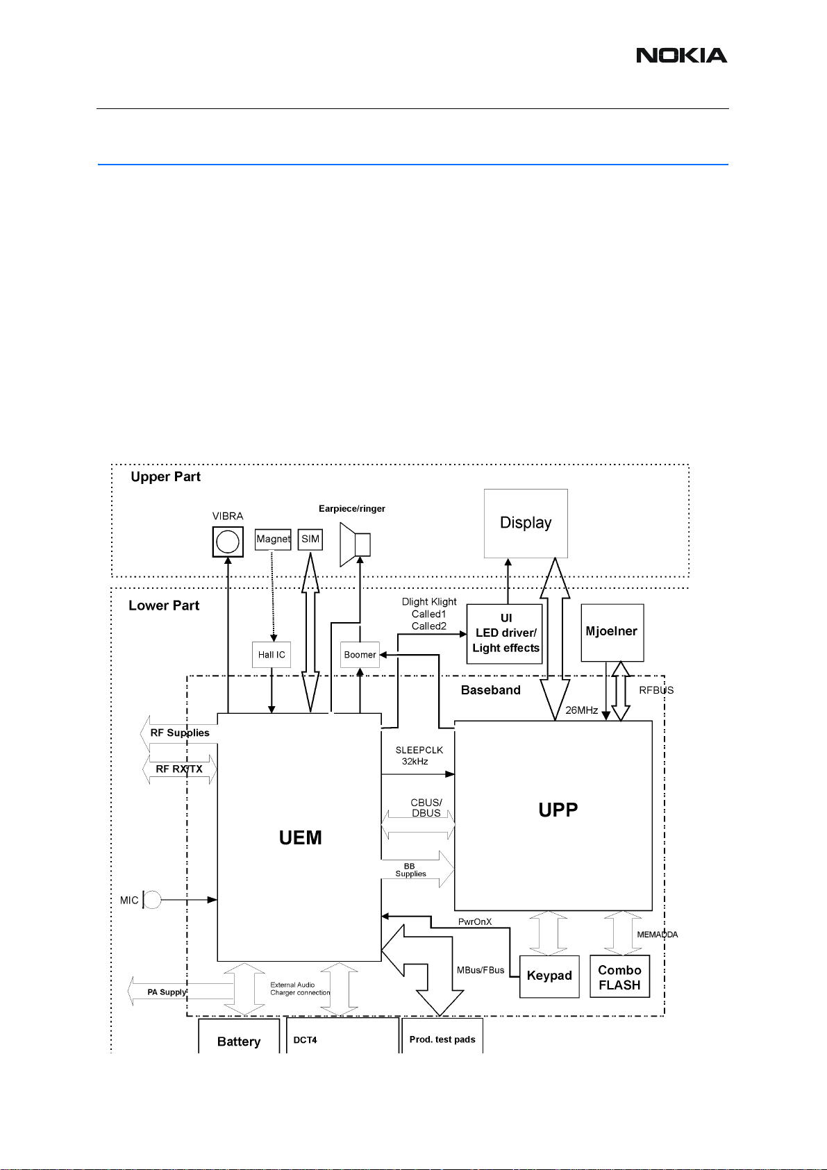
Introduction
This document specifies the baseband module for the RH-53/54 platform program. The baseband module includes the baseband engine chipset, the UI components and the acoustical
parts for the transceiver.
RH-53/54 is a hand-portable dualband GSM/GPRS 900/1800MHz fold-phone, having the
DCT4 generation baseband (UEM/UPP) and RF (MJOELNER) circuitry. The RH-53 platform
also supports a GSM 850/1900 US variant called RH-54. RH-53 platform is based on common
baseband engine 4.0.
■ Technical Summary
The baseband module contains 2 main ASICs named the UEM and UPP. The module furthermore contains a Combo Flash IC of 64Mbit flash and 16Mbit RAM.
Figure 1:RH-53/54 bb block diagram
Interface
ISSUE 1 09/2004 COMPANY CONFIDENTIAL 9
Copyright © 2004 Nokia. All Rights Reserved.
Page 10

RH-53/54
Nokia Customer Care 8-System Module
The UEM supplies both the baseband module as well as the RF module with a series of voltage
regulators. Both the RF and baseband modules are supplied with regula ted voltages of 2.78 V
and 1.8V. UEM includes 6 linear LDO (low drop-out) regulators for baseband and 7 regulators
for RF. The UEM is furthermore supplying the baseband SIM interface with a programmable
voltage of either 1.8 V or 3.0 V. The core of the UPP is supplied with a programmable voltage
of 1.0 V, 1.3 V, 1.5 V or 1.8 V.
UPP operates from a 26MHz clock, coming from the RF ASIC MJOELNER, the 26 MHz clock
is internally divided by two, to the nominal system clock of 13MHz. DSP and MCU contain
phase locked loop (PLL) clock multipliers, which can multiply the system fr equency by factors
from 0.25 to 31.
The UEM contains a real-time clock, sliced from the 32768 Hz crystal oscillators. The 32768
Hz clock is fed to the UPP as a sleep clock.
The communication between the UEM and the UPP is done via the bi-directional serial busses
CBUS and DBUS. The CBUS is controlled by the MCU and operates at a speed of 1 MHz set
by SW. The DBUS is controlled by the DSP and operates at a speed of 13 MHz. Both processors are located in the UPP.
The UEM ASIC handles the interface between the baseband and the RF section. UEM provides A/D and D/A conversion of the in-phase, quadrature receive/transmit signal paths and
also A/D and D/A conversions of received and transmitted audio signals to and from the user
interface. The UEM supplies the analog signals to RF section according to the UPP DSP digital
control. RF ASIC MJOELNER is controlled through UPP RFBUS serial interface. There are
also separate signals for PDM coded audio. Digital speech processing is handled by the DSP
inside UPP ASIC.
UEM is a dual voltage circuit, the digital p art s ar e running from the baseband supply 1 .8V and
the analog parts are running from the analog supply 2.78V also VBAT is directly used by some
blocks.
The baseband supports both internal and external microphone inputs and speaker outputs.
RH-53/54 has two external serial control interfaces: FBUS and MBUS. These busses can be
accessed through production test pattern as described in section 8.
RH-53/54 transceiver modules are implemented on 8 layers and the surface are with selective
Ni/Au OSP.
■ List of Features
RH-53 platform common features:
• Jack UI style 20 keys (with 4 ways scroll) ESD-proof layout, multiple keypress.
• Battery BL-4C
•UEMK
• UPP8Mv2.6/2.10 Lead Free
• Combo Flash 8MByte flash memory and 2MByte PSRAM (64Mbit+16Mbit)
• Power key integrated in keypad (common with End key)
• Internal vibra
• Colour display (colures 4096, resolution: 130 columns x 130 rows, technology:
CSTN)
10 COMPANY CONFIDENTIAL ISSUE 1 09/2004
Copyright © 2004 Nokia. All Rights Reserved.
Page 11

RH-53/54
8-System Module Nokia Customer Care
• Polyphonic ringing tones
• 2 white LED’s for LCD Backlight.
• 2 white LEDs for key mat & 3 blue LED’s for Light-effect in key mat.
•JAVA
•MMS
•GPRS
ISSUE 1 09/2004 COMPANY CONFIDENTIAL 11
Copyright © 2004 Nokia. All Rights Reserved.
Page 12

RH-53/54
Nokia Customer Care 8-System Module
Technical Specifications
■ Modes of Operation
RH-53/54 baseband engine has six different ‘normal’ operating modes:
• Νo supply
• Power off
• Αcting dead
•Active
•Sleep
• Charging
No supply
In this mode the phone has no supply voltage.
The phone enters this mode if the battery is disconnected, or the battery voltage drops below
V
MSTR-
(1.8V~2.0V)
The phone exits ‘No supply’ mode, into hardware ‘Reset’ mode (not described here), after a
20ms delay, if the battery voltage rises above V
placing the battery with a new battery (V
the battery above V
MSTR+
.
BAT>VMSTR+
(2.0~2.2V). This will occur either by re-
MSTR+
), or by connecting a charger and charging
The phone exits ‘Reset’ mode into ‘Active’/Acting dead’ mode when the battery voltage rises
above V
V
COFF-
V
COFF+
COFF+
(2.7~2.9V) for a minimum of 240.5ms. If the battery voltage has not risen beyond
before the internal watchdog elapses the phone is forced into ‘Power of f’ mode instead.
(3.0~3.2V) within the watchdog time period, and subsequently stays above
Power off
In this mode the phone is powered off, but has a supply voltage.
The phone enters ‘Power off’ mode from all other modes, except ‘No su pply’, if internal watch-
dog elapses. VRTC regulator is active (enabled), and supplied from the main batte ry (the RTC
status depends on whether RTC was enabled or not when entering ‘Power off’ mode).
The phone exits ‘Power off’ mode, into hardware ‘Reset’ mode (not described here), after a
20ms delay, if either of the following conditions are met:
• Power on button detected (PwrOffX).
• Charger connection detected (VCharDet)(VCharIn>VCH
(1.9~2.1V)).
DET+
• RTC alarm detected (RTC_ALARM).
The phone exits ‘Reset’ mode into ‘Active’/Acting dead’ mode when the battery voltage rises
above V
12 COMPANY CONFIDENTIAL ISSUE 1 09/2004
, and stays above V
COFF+
for a minimum of 240.5ms.
COFF-
Copyright © 2004 Nokia. All Rights Reserved.
Page 13

RH-53/54
8-System Module Nokia Customer Care
Acting dead
This mode is just a sub mode of normal ‘Active’ mode, where everything, except for VSIM and
the RF parts, is powered up. This mode is only used for when t he phone is in ‘Power off’ or ‘No
supply’ mode and a charger is connected. To the user , the phone act s as if it was switched off.
A battery-charging alert is given and/or a battery charging indication on the display is shown,
to acknowledge the user that the battery is being charged. The software differentiation betwe en
‘Acting dead’ and ‘Active’ is based on whether or not a power on button was initially detected
(PwrOffX).
The phone exits from ‘Power off’ or ‘No supply’ mode, into hardware ‘Reset’ mode (not described here), after a 20ms delay, if a charger connection is detected (VCharDet)(VCharIn>VCH
The phone then enters ‘Acting dead’ mode, after a 100ms delay, if the battery voltage rises
above V
COFF+
(sub mode of normal ‘Active’).
The phone exits ‘Acting dead’, into ‘Active’ mode, if the power on button is detecte d (PwrOffX).
DET+
).
Active
In the active mode the phone is in normal operation, scanning for channels, listening to a base
station, transmitting and processing information. There are several sub-states in the active
mode depending on if the phone is in burst reception, burst transmission, if DSP is working, if
the phone is folded or unfolded etc.
In active mode the RF regulators are controlled by SW writing into UEMK’s registers wanted
settings: VR1B must be kept disabled. VR2 can be enabled or forced into low quiescent current
mode. VR3 is always enabled in active mode. VR4 -VR7 can be enabled, disabled or forced
into low quiescent current mode.
Sleep mode
The phone enters ‘Sleep’ mode when the UPP goes into standby mode and forces the UEM
into sleep mode by pulling SleepX low.
The UEM puts VCORE, VIO and VFLASH1 into sleep mode an d disables VANA and all of the
RF regulators except VR2, VSIM is also put into sleep mode if supported by the SIM card. The
main oscillator (26MHz) is also shut down and the 32 kHz sleep clock oscillator is used as reference clock for the baseband.
The phone exits sleep mode when SleepX is set high by the UPP, or by expiration of a sleep
clock counter in the UEM or by some external interrupt, generated by a charger connection,
key press, headset connection etc.
Charging
Charging can be performed in parallel with any other operating mo de. The charging will be controlled by hardware until the phone enters either ‘Sleep’, ‘Acting dead’ or ‘Active’ mode. Hereafter it will be controlled by software.
ISSUE 1 09/2004 COMPANY CONFIDENTIAL 13
Copyright © 2004 Nokia. All Rights Reserved.
Page 14

RH-53/54
Nokia Customer Care 8-System Module
A BSI resistor inside the battery pack indicates the battery type/size. The resistor value corresponds to a specific battery capacity and technology.
The battery voltage, temperature, size and current are measured by the UEM, and controlled
by the charging software running in the UPP.
The charging control circuitry (CHACON) inside the UEM controls the charging current delivered from the charger to the battery. The battery voltage rise is limited by turning the UEM
switch off when the battery voltage has rea ched VBATLim (programmable charging cut-off limits 3.6V / 5.0V / 5.25V). Charge current is monitored by measuring the voltage drop across a
0.22 ohm resistor.
■ Regulators
Overview of the regulator state in ‘Active’, ‘Acting dead’ and ‘Sleep’ mode is shown in table 1.
Table 1: Overview
Regulator Active Acting dead Sleep
VFLASH1 Enabled Enabled Sleep mode
VFLASH2 Disabled (Not used) Disabled (Not used) Disabled (Not used)
VANA Enabled Enabled Disabled
VIO Enabled Enabled Sleep mode
VCORE Enabled Enabled Sleep mode
VSIM Enabled (voltage control-
led by software)
VR1A Enabled Enabled Disabled
VR1B Disabled (Not used) Disabled (Not used) Disabled (Not used)
VR2 Enabled (voltage control-
led by software)
VR3 Enabled Disabled Disabled
VR4 Disabled Disabled Disabled
Disabled Enabled/Sleep mode
(depending on SIM
card)
Enabled (voltage controlled by software)
Enabled (voltage controlled by software)
VR5 Enabled Disabled Disabled
VR6 Enabled Disabled Disabled
VR7 Enabled Disabled Disabled
Regulator Active Acting dead Sleep
IPA1-2 Disabled (not used) Disabled (not used) Disabled (not used)
14 COMPANY CONFIDENTIAL ISSUE 1 09/2004
Copyright © 2004 Nokia. All Rights Reserved.
Page 15

RH-53/54
8-System Module Nokia Customer Care
■ DC Characteristics
Supply Voltage Ranges
Table 2: Supply voltage ranges
Signal Rating
Battery Voltage 0 ... 4.39V (VBAT)
Flashing Voltage 0 … 5.15V
Charger Input Voltage -0.3 ... 9.2VRMS (16,9 Vpeak)
Following voltages are assumed as normal and extreme voltages for used battery:
Table 3: Battery voltages
Source Min Nom Max Note
VBAT 3.21V 3.80V 4.39V 1
Vcoff+ 3.0V 3.1 3.2 HW off to on
Vcoff- 2.7V 2.8V 2.9V HW on to off
Vmstr+ 2.0V 2.1V 2.2V HW off to on
Vmstr- 1.8V 1.9V 2.0V HW on to off
Sw shutdown - 3.1V - In Call
1 TA will test with the nominal voltage at an 85% range (0.85 x 3.7V = 3.145V); therefore the
nominal voltage has been set to 3.8V. ADC settings in the SW might shutdown the phone
above the min value. During fast charging of an empty battery, the max voltage might exceed
this value. Voltages between 4.20 and 4.60 might appear for a short while.
ISSUE 1 09/2004 COMPANY CONFIDENTIAL 15
Copyright © 2004 Nokia. All Rights Reserved.
Page 16

RH-53/54
Nokia Customer Care 8-System Module
Regulators Voltage Ranges
Table 4: Regulators voltage ranges
Source Min Nom Max Note
VANA 2.70V 2.78V 2.86V I
VFLASH1 2.70V 2.78V 2.86V I
max
max
I
sleep
= 80mA
= 70mA
= 4mA
VFLASH2 2.70V 2.78V 2.86V Not used
VSIM 1.745V 2.91V 1.8V 3.0V 1.855V 3.09V I
max
I
sleep
= 25mA
=
0.5mA
VIO 1.72V 1.8V 1.88V I
max
I
sleep
= 150mA
=
0.5mA
VCORE Higher
range
1.000V 1.140V
1.235V 1.425V
1.710V
1.053V 1.2V 1.3V
1.5V 1.8V
1.106V 1.260V
1.365V 1.575V
1.890V
= 200mA
I
max
I
=
Sleep
0.2mA Used
voltages:
(c035) = 1.5V
(c027) = 1.3V
Table 5: RF regulators
Source Min Nom Max Note
VR1A 4.6V 4.75V 4.9V Imax = 10mA
VR1B 4.6V 4.75V 4.9V Not used
VR2 2.70V 2.78V 2.86V I
VR3 2.70V 2.78V 2.86V I
= 100mA
max
= 20mA
max
VR4 2.70V 2.78V 2.86V Not used
VR5 2.70V 2.78V 2.86V I
VR6 2.70V 2.78V 2.86V I
VR7 2.70V 2.78V 2.86V I
= 50mA
max
= 50mA
max
= 45mA
max
16 COMPANY CONFIDENTIAL ISSUE 1 09/2004
Copyright © 2004 Nokia. All Rights Reserved.
Page 17

RH-53/54
r
8-System Module Nokia Customer Care
■ Interconnection Diagram
Figure 2:IPower distribution diagram
Battery
Baseband
LED+
LED
Driver
VBAT
UEM
RF Regulators
Baseband
Regulators
RTC
CHACON
VR1A
VR2-7
VSIM
VCORE
VANA
VIO
VFLASH1
6
SIM
UPP
FLASH
LCD
Boomer
PA Supply
System Connecto
■ External Signals and Connections
Battery connector
As a difference to previous NMP Battery Interfaces, BTEMP has been removed and battery
temperature is estimated by measurement in Transceiver PWB with a separate NTC resistor.
Thus the Battery Interface has only 3 contact s. BSI ranges has been a ltered and Battery Int erface will not support NiMh batteries.
Table 6: Battey connetor
Name Description Test usage
VBAT Battery voltage terminal. Battery calibration.
GND Battery ground terminal.
BSI Battery size identification. Flash and local mode forcing.
ISSUE 1 09/2004 COMPANY CONFIDENTIAL 17
Copyright © 2004 Nokia. All Rights Reserved.
Page 18

RH-53/54
Nokia Customer Care 8-System Module
Baseband - RF interface
The interface between the baseband and the RF can be divided into three categories:
- The digital interface from the UPP to the RF ASIC (Mjoelner). The serial digital interface is
used to control the operation of the different blocks in the RF ASICs.
- The analogue interface between UEM and the RF. The analogue interface consists of RX and
TX converter signals. The power amplifier control signal TXC and the AFC signal comes as well
from the UEM.
- Reference clock interface between Mjoelner and UPP, which supplies the 26Mhz system
clock for the UPP.
■ Internal Signals and Connections
The tables below describe internal signals. The signal names can be found on the schematic
for the PWB.
Audio
Table 7: Internal microphone
Signal Min
MIC1P (Differential input P) - 5mV - TBD
MIC1N (Differential input N) - 5mV - TBD
MICB1 (Microphone Bias) 2.0 V2.1 V2.25 V DC
External loading of MICB1 - - 600uA DC
Table 8: Internal speaker (Differential output EARP & EARN)
Signal Min
Output voltage swing 4.0 - - Vpp Differential output
Load Resistance (EARP to
EARN)
Load Capacitance (EARP to
EARN)
25,5 27,228,9 W 2*10Ù 5% +
- - 50 nF
No
m
No
m
Max
Max Units Note
Conditi
on
Note
7,2Ù±10%
18 COMPANY CONFIDENTIAL ISSUE 1 09/2004
Copyright © 2004 Nokia. All Rights Reserved.
Page 19

RH-53/54
8-System Module Nokia Customer Care
Speaker (Ringer & Earpiece)
Table 9: Connections between UPP and Boomer
Signal From To Parameter Min. Max. Unit Notes
Shutdown
(Only
Ringer)
UPP
GENIO[14
]
Boomer
Shutdown (pin
5)
Table 10: Connections between UEM/Battery and Boomer
Signal
name
XAUDIO[1] Filtered
signal
Differential
between HF and
HFCM. No direct
connection
From To
BoomerOutput
between UEM
and Boomer
VBAT Battery Boome
r (pin 6)
Hinge flex connection
Vih Vil 1.2 - - 0.4 V V Boomer
Shutdown
treshold
levels
Paramete
r
Min. Max. Unit Notes
- 80mV Vpp Long-term
Swing
consumption
Supply 3.2 4.39 V Lower limit
is SW cutoff
Connection between main engine (lower block) and upper is done by hinge flex via 30 pins
board to board connector . Hinge flex includes Earpiece/Ringer, Display , SIM, LCD led and Vibra signals.
Table 11: Hinge flex signals
Pin Signal Comments
1,2,3,4 GND
5 LCD_CSL Display Serial Clock
6 LCD_CSX Display Chip Select
7,8,9 GND
10 Vibra PWM signal
11 Vbat For Vibra
12,13,14,15 GND
16 SIMCAR D_Det Detection of SIM Card
17 VSIM 3.0V/1.8V for SIM
18 SIM_RST SIM Reset
19 SIM_IO SIM Data
20 SIM_CLK SIM Clock
ISSUE 1 09/2004 COMPANY CONFIDENTIAL 19
Copyright © 2004 Nokia. All Rights Reserved.
Page 20

RH-53/54
Nokia Customer Care 8-System Module
Pin Signal Comments
21 GND
22 EARP For MALT
23 EARN For MALT
24 GND
25 VDD "Vflash1" 2. 78 V for Display
26 LED- Return from LEDs
27 LED+ Pos supply for LEDs
28 VDDI "Vio" 1.80 V for Display
29 LCD_RESETX Display Reset
30 LCD_SI Display Serial Data
Figure 3:Flex con. pin out
Pin 30 Pin 1
20 COMPANY CONFIDENTIAL ISSUE 1 09/2004
Copyright © 2004 Nokia. All Rights Reserved.
Page 21

RH-53/54
8-System Module Nokia Customer Care
■ Baseband board clocks
Table 12: Board Clocks
Signal name From To Min. Typ. Max. Unit Notes
RFCLK MJOEL-
NER
SLEEPCLK UEM UPP - 32.768 - KHz Active when
RFCONVCLK
RFBUSCLK UPP MJOEL-
DBUSCLK UPP (DSP) UEM - 13 13 MHz Only active
CBUSCLK UPP (MCU) UEM - 1 1.2 MHz Only active
LCDCAMCLK
UPP UEM 13 - MHz Active when RF
UPP LCD 0.3 6.25 8.4 MHz Only active
UPP - 26 - MHz Active when
SLEEPX is high
VBAT is supplied
converters are
active
- 13 13 MHz Only active
NER
when bus-enable is active
when bus-enable is active
when bus-enable is active
when bus-enable is active
MemClk/
Flash
UPP Flash 40 MHz
ISSUE 1 09/2004 COMPANY CONFIDENTIAL 21
Copyright © 2004 Nokia. All Rights Reserved.
Page 22

RH-53/54
Nokia Customer Care 8-System Module
Functional Description
Audio External
RH-53/54 is designed to support fully differentia l external audio accessory connection. A headset and PnPHF can be directly connected to system connector. Detection of the different accessories is made in analog way by reading the DC voltage value of EAD converter.
Figure 4:External audio interface
2.7V
Hookint
/MBUS
Headint Headint
HFCM
EAD
Mic_bias
HF
UEM
MICB2
MIC2P
MIC2N
3...25k
Headset Detection
Not all components are shown
Bottom
Connector
33N
1k0
1k0
0.3V
1.8V
2.1V
33N
0.8V
0.8V
MicGnd
Supported headsets are 4-wire fully differential accessories. The hardware used to detect accessories is contained in the UEM and BB area. For interrupt purposes the UEM inputs
HOOKINT and HEADINT are used. The bottom connector contains a switch, which opens
when an accessory is connected. The switch is routed to the UEM HEADINT input.
The current generators on the HOOKINT and HEADINT pins acts as internally pull-up resistors
with values equivalent to 675 k - 2.86 M, tolerances of the current source and VFLASH1 considered. The HOOKINT input comparator threshold level can be set to two different values.
Levels can be found in the table.
Table 13: Comparator threshold levels and pull-up current source strength (hysteresis included)
Parameter Variable Min Typ Max
HOOKINT comparator thresh-
Vhook1 1.21 V 1.35 V 1.49 V
old
22 COMPANY CONFIDENTIAL ISSUE 1 09/2004
Copyright © 2004 Nokia. All Rights Reserved.
Page 23

RH-53/54
8-System Module Nokia Customer Care
HOOKINT comparator threshold
HEADINT comparator threshold
VFLASH1 voltage regulator VFLASH1 2.70 V 2.78 V 2.86 V
Current source strength Ipullup 1 µA2 µA4 µA
Note that hysteresis of the comparators has been taken into account in the HOOKINT
and HEADINT Min and Max values.
Vhook2 0.50 V 0.60 V 0.70 V
Vhead 1.71 V 1.90 V 2.09 V
PnPHF Detection
PnPHF accessory uses 4-wire fully differential audio connection. The a ccessory is detected by
the Headint signal when the plug is inserted.
■ Audio Internal
Earpiece/Ringer
The choosen transducer that shall be used both as earpiece and ringer is the 16 mm loudspeaker called MALT.
The Earpiece/ringer solution will be build up around the 16 mm MALT speaker that shall be
used both as earpiece and ringer. This solution will implement polyphonic ringing tones.
The earpiece circuit includes only a few components:
-Two 10 ohm in order to have a stable output
The ringer circuit includes several components
-Four resistors for setting the boomer gain
ISSUE 1 09/2004 COMPANY CONFIDENTIAL 23
Copyright © 2004 Nokia. All Rights Reserved.
Page 24

RH-53/54
Nokia Customer Care 8-System Module
Figure 5:Earpiece/ringer interface
UEM
EARP
EARN
10
10
HF
HFCM
UPP
GENIO14
Interface to
external audio
100n
100n
XEARP
XEARN
Vbat
Vdd
GND
33k
330p
Vo1
Vo2
Placed near
UEM
Placed outside
BB-can, near the
connections to
MALT
MALT
Interface to
DC-out
Not used / NA
1u
4k7
4k7
330p
33k
470 n
IN-
IN+
BYPASS
SHUTDOWN
Microphone
The acoustical design is copied from Nokia 7210 with some modifications. In comparison to
N7210, the microphone boot is a separate component placed next to the bottom connector.
The electrical Microphone design is a differential bias circuit, driven directly from the MICB1
bias output with external RC-filters. This is one solution that has previously been used with success in other projects.
The RC filter (220 Ω, 4.7µF) is scaled to provide damping at 217 Hz. TDMA noise (217 Hz au-
dible noise) will occur if the bias output MICB1 demodulates in-coming radio frequencies.
Common DCT4 BB specifies filtering of the reference voltage for the microphone bias gene rators. In next figure this filtering is included on the MICBCAP pin. This capacitor will not be
mounted when the UEMc will be used.
The microphone bias is controlled in the 8 bit AudioBiasR register . The figure below shows the
electrical interface.
24 COMPANY CONFIDENTIAL ISSUE 1 09/2004
Copyright © 2004 Nokia. All Rights Reserved.
Page 25

RH-53/54
8-System Module Nokia Customer Care
Figure 6:Microphone interface
Placed near
bottom
connector
UEM
Placed near
UEM
1n 1n
1k
10n
2k2
2k2
1k
10n
MIC+
1n
MIC-
MICB1
MIC1P
MIC1N
MICBCAP
220
4.7uF
2k2
2k2
1u
22k
2*33n
■ Vibra
Introduction
Vibra is a small cylindrical DC motor with a ∅4.0-mm in diameter that generating vibration by
rotating an un-balanced mass (counter weight) with radius of R=2.5-mm when the applied voltage is on.
The vibration signal will be used as a silent alert call and also as a noticeable shock in gaming.
Acoustic design
The vibra is placed in the top of the phone when it is fold/closed but it placed under the display
when it is unfold. The counter weight is placed in the top middle (unfold) that may results to
shorter distance to the mass center of the phone. This mechanical solution will result to lower
vibration/velocity amplitude, as the axel of torque is shorter.
The vibra is electrically connected to the flexfilm by spring contacts.
The vibra is controlled from the UEMK by a PWM (Pulse Wide Modulated) square wave signal.
The nominal rated voltage for the vibra is approximately about 1.3 volts and the nominal battery
voltage is about 3.6 volts. To achieve an optimal voltage over the vibra, the following table
should be used.
■ Batteries
Type:BL-4C battery
Technology:Li-Ion. 4.2V charging. 3.1V cut-off
Capacity:760 mA/h
ISSUE 1 09/2004 COMPANY CONFIDENTIAL 25
Copyright © 2004 Nokia. All Rights Reserved.
Page 26

RH-53/54
Nokia Customer Care 8-System Module
Figure 7:BL-4C battery
The BSI values for the batteries:
Inside the battery, an over-voltage protection circuit are present.
The battery does not contain a temperature sensor. Since the battery is using the Li-Ion tech-
nology , care should be t aken while charging. The material might be overheated when charged
above 60 degrees Celsius. Charging should be termina ted when this temperature is reached.
An external temperature sensor (NTC resistor) is placed on the PWB close to the end of the
battery. Real measurements should be performed to check if the location is sufficient.
■ Keyboard
The keyboard PWB layout consists of a grounded outer ring and an inner pad see Figure 8.
Figure 8:Keyboard PWB layout
The keyboard is not a matrix keyboard, but is connected direct to UPP. The following table
shows the keyboard connection.
Table 14:
UPP Pin RH-53 Key
GenIO1 0 In Up GenIOInt5 Falling edge interrupt
GenIO2/
P05
GenIO20 Soft Right In Up GenIOInt2 Falling edge interrupt
7 In Up P0 int Falling edge interrupt
Overview of keyboard configuration
In/
Out
Internal Pull
Up/down
Interrupt
GenIO21 * In Up GenIOInt3 Falling edge interrupt
GenIO25 Up In Up GenIOInt4 Falling edge interrupt
GenIO27 1 In Up GenIOInt6 Falling edge interrupt
26 COMPANY CONFIDENTIAL ISSUE 1 09/2004
Copyright © 2004 Nokia. All Rights Reserved.
Page 27

RH-53/54
8-System Module Nokia Customer Care
GenIO28 Left In Up GenIOInt7 Falling edge interrupt
GenIO13 # In Up GenIOInt1 Falling edge interrupt
P00 Send In Up P0 int Falling edge interrupt
P01 3 In Up P0 int Falling edge interrupt
P02 9 In Up P0 int Falling edge interrupt
P03 8 In Up P0 int Falling edge interrupt
P04 Down In Up P0 int Falling edge interrupt
P10 6 In Up P1 int Falling edge interrupt
P11 4 In Up P1 int Falling edge interrupt
P12 Righ t In Up P1 int Falling edge interrupt
P13 5 In Up P1 int Falling edge interrupt
P14 Soft Left In Up P1 int Falling edge interrupt
P15 2 In Up P1 int Falling edge interrupt
UEM Pin
PwrOnX End / power
on/off
NOTES:
• Key number “#” is located on GenIO13 with interrupt on GenIOInt1. RH-53 Marketing accept the reduction in performance when there is no wake up from deep
sleep.
• Power on/off and End Call are combined. For ending call: “short” keypress. For
power off: “Long” keypress
All lines are configured as input, when there is no key pressed; the inputs are high due to that
the UPP has internally pull-up resistors on those lines. When a key is pressed, the specific line
where the key is placed is pulled low . This generates an interrupt to the MCU and the MCU now
starts its scanning procedure.
In Current source
Pull up
INT on UPP Falling edge interrupt
■ Display & Keyboard Backlight
LCD Backlight
LCD Backlight consists of 2 side firing white LED's, which are placed on the display FPC below
the LCD area.
Keyboard light effects
Keyboard is lighting up by 2 white side firing LED’s for keyboard. 3 blue LED’s are used for Light
effects in the keyboard.
ISSUE 1 09/2004 COMPANY CONFIDENTIAL 27
Copyright © 2004 Nokia. All Rights Reserved.
Page 28

RH-53/54
Nokia Customer Care 8-System Module
■ LCD
The LCD display module is a 130 x 3RGB x 130, 4096-color/ 256-color /8-color transflective
passive matrix (CSTN) LCD display.
The LCD module interface follows 130x130 X4_CSTN Display module interface specification
(Nokia doc. Code: DHS02040-EN 0.2). Nile display family is using serial interface only
■ Memory Module
The RH-53/54 baseband memory module consists of external burst NOR flash memory 8Mbyte
(64Mbit) and CMOS 2Mbyte (16Mbit) PSRAM
The flash interface follows the common baseband interface.
The operations voltage is Vcc=1.8 V (Voltage range 1.7-1.9 V).
■ Fold detection-switch
Detection for fold position has been done with HALL- switch SH248CSP which is located in lower block part and the magnet is located on upper block.
The output is high level for B=0mT (flip open).
■ SIM Interface
The SIM interface can be described as electrical interface between the SIM card and the phone
via UEM. The SIM interface in the UEM contains power up/down, port gating, card detect, data
receiving, ATR-counter, registers and level shifting buffers logic.
Figure 9:UEM, UPP and SIM interface
C4 C3 C2 C1
C5 C6 C7 C8
SIM Card
Passive
filter
SIMIO
SIMclk
SIMRST
VSIM
SimCardDet
UEM
SIMIO
SIMclk
SIMRST
SIM IF
Register
UEM
Digital
Logic
UPP
SIMIO
SIMclk
SIMR
UIF block
UEM int
Cbus Da
Cbus enX
Cbus clk
The data communication between the card and the phone is asynchronous half duplex. The
clock supplied to the card in GSM system is either 1.083 MHz or 3.25 MHz. The dat a baud rate
is SIM card clock frequency divided by 372 (by default), 64, 32 or 16.
28 COMPANY CONFIDENTIAL ISSUE 1 09/2004
Copyright © 2004 Nokia. All Rights Reserved.
Page 29

RH-53/54
8-System Module Nokia Customer Care
SIM -reader
The SIM card reader is located on upper block p art of the phone and is connected to UEM via
the flex. For RH-53 a slide-in draw is used as SIM slot. Picture below depicts the SIM slot on
the side of the upper block.
Figure 10:Upper block B-cover SIM-slide slot
The entire SIM interface is located in the two ASICs, UPP and UEM. The UEM contains the
SIM interface logic level shifting. The SIM interface can be programmed to support 3 V and 1.8V
SIMs. A register in the UEM controlled by SW is used to select s SIM supply voltage for different
SIMs. However, it is only allowed to change the SIM supply voltage when the SIM IF is initialised i.e. SIM IF id powered down.
Of the eight card contacts only 5 will be connected: C1 (Vcc), C2 (Card Reset), C3 (Card
Clock), C5 (Ground) and C7 (Data I/O).
SIM switch and card detection
The SIM power up/down sequence is generated in the UEM. This means that the UEM gen erates the RST signal to the SIM. A mechanical switch is connect ed to UEM SimCardDet pin to
monitor the presence of the SIM card, i.e. card detection. When the SIM card is inserted, the
switch connects the SimCardDet to GND.
To avoid probable SIM card corruption caused by “hot-swapping”, the UEM will automatically
power down the SIM card interface within 2ms if the switch is opened.
ISSUE 1 09/2004 COMPANY CONFIDENTIAL 29
Copyright © 2004 Nokia. All Rights Reserved.
Page 30

RH-53/54
Nokia Customer Care 8-System Module
Figure 11:SIM draw and switch
30 COMPANY CONFIDENTIAL ISSUE 1 09/2004
Copyright © 2004 Nokia. All Rights Reserved.
Page 31

RH-53/54
8-System Module Nokia Customer Care
Assembly
■ Flex
RH-53/54 uses a single layer flex with ground tracks distributed between signal groups, and
wide ground tracks running in both sides of the flex to serve as main ground.
ISSUE 1 09/2004 COMPANY CONFIDENTIAL 31
Copyright © 2004 Nokia. All Rights Reserved.
Page 32

RH-53/54
Nokia Customer Care 8-System Module
Security
The phone flash program and IMEI code are software protected, using an external security device that is connected between the phone and a PC. The security device uses IMEI number
(IMEI is stored in UEM non-volatile memory cells), the software version number and a 24bit
hardware random serial number that is read from the UPP, and calculates a flash authority
identification number, that is stored into the phone (emulated) EEPROM.
32 COMPANY CONFIDENTIAL ISSUE 1 09/2004
Copyright © 2004 Nokia. All Rights Reserved.
Page 33

RH-53/54
8-System Module Nokia Customer Care
Test Interfaces
Test pattern is placed on engine PWB, for service and production purposes, same test pattern
is used for after sales purposes as well.
Through MBUS or FBUS connections, the phone HW can be tested by PC software (Phoenix)
and equipment (FLALI/FINUI/LABEL).
Figure 12: Test pattern
Figure 1 Production test pattern J396 (DAI is J300)
DAI
GND
FBUS RX
FBUS TX
MBUS
Vpp
■ Connections to Baseband
The flash programming box, FPS8, is connected to the baseband using a galvanic connector
or test pads for galvanic connection. The UEM watchdog is disabled during flash programming
to prevent a hardware reset of the timer. The flash programming interface connects the flash
prommer to the UPP via the UEM and the connections correspond to a logic level of 2.7 V . The
flash prommer is connected to the UEM via the MBUS (bi-directional line), FBUS_TX, and
FBUS_RX. The programming interface connections between the UEM and the UPP constitute
the MBUS_TX, MBUS_RX, FBUS_TX, and FBUS_RX lines. The interface also uses the BSI
ISSUE 1 09/2004 COMPANY CONFIDENTIAL 33
Copyright © 2004 Nokia. All Rights Reserved.
Page 34

RH-53/54
Nokia Customer Care 8-System Module
(Battery Size Indicator) and the PURX signal connections for the connections between the
UEM and the UPP.
■ FBUS Interface
FBUS is an asynchronous data bus having separate TX and RX signals. Default bit rate of the
bus is 115.2 kbit/s. FBUS is mainly used for controlling phone in the production. Typical
VFLASH1 is 2.78V
Table 15: FBUS interface signals
Signal Min Nom Max
FBUS_TX Voh 0.7*VFLASH1 VFLASH1
Vol 0 0.3*VFLASH1
FBUS_RX Vih 0.7*VFLASH1 VFLASH1
Vil 0 0.3*VFLASH1
TX and RX
Tr 12.5 ns
Rise time
GND 0
■ Test points
The following table show the test points on the main board.
Table 16: Test points
Test point: Description:
J100 Vbatt on battery connector
J101 BSI on battery connector
J102 GND on battery connector
J300 DAI_CLK on production test pattern
J150 GENIO 14 (Boomer)
J002 DLight
J303 Keyb1 (output from Hall IC)
J396 Production test pattern (see
14
)
Figure
J402 PURX (UPP)
J403 SLEEPX (UPP)
34 COMPANY CONFIDENTIAL ISSUE 1 09/2004
Copyright © 2004 Nokia. All Rights Reserved.
Page 35

RH-53/54
8-System Module Nokia Customer Care
J404 SLEEPCLK (UPP)
J405 UEMINT (UPP)
J406 CBUSCLK (UPP)
J407 CBUSDA (UPP)
J408 CBUSENX (UPP)
J409 MBUSTX (UPP)
J410 MBUSRX (UPP)
J411 FBUSTX (UPP)
J412 FBUSRX (UPP)
J413 DBUSCLK (UPP)
J414 DBUSDA (UPP)
J415 DBUSEN1X (UPP)
J416 EXTWRX (UPP)
J417 EXTRDX (UPP)
J418 FLS2CSX (UPP)
J419 FLSCLK (UPP)
J420 FLSCSX (UPP)
J421 RFBUSCLK
J422 RFBUSDA
J423 RFBUSEN1
J424 GENIO 7 (BB-RF Interface)
J600 RXIP (Mjoelner)
J601 RXIM (Mjoelner)
J602 RXQP (Mjoelner)
J603 RXQM (Mjoelner)
ISSUE 1 09/2004 COMPANY CONFIDENTIAL 35
Copyright © 2004 Nokia. All Rights Reserved.
Page 36

RH-53/54
Nokia Customer Care 8-System Module
RF Functional Descriptions
■ RF block diagram
Block diagrams of direct conversion receiver and transmitter RF section has described in the
following figure.
The architecture is based on Mjoelner , the RF ASIC, which contains most of the functionality of
the RF Engine. The ASIC contains RX and TX functions, VCXO (crystal is placed external to
the ASIC), se the block diagram.
Figure 13:RF block diagram
Pinocchio RF block diagram
RX/TX switch
PA and detector
Vapc
VBATTRF
Diplexer
Vsense
Version : 0.1
Ant
SAW
INPL
RX900
INML
GSM RX
PCS RX
TX/RX GSM
TX/RX DCS
VTX
Band sel
PCN/PCS
GSM
SAW
PCN/PCS
Balun
VTX
SAW
PWloop
filter
RX1800/
1900
VPCTRL_G
INPM
INPH
INMH
VANTL
VANTM
VANTH
VB_DET
VTXLOL
VTXLOH
VTXBH
VTXBL
OUTHP
OUTHM
OUTLP
OUTLM
DET
PLFB1
PLFB2
INMM
LNA
Bias
ASIC
LNA
LNA
LNA
RF
Controls
RF
Controls
Open collector
Open collector
PWC
TXP
TXP
F
X
R
D
D
V
VDDDIG
VDDRXBB
TXC
TXC
Pre-gain
Pre-gain
Supply
filter
VR2
VDDTX
VTX
Rx
supply
filter
222
2
1/2
1/2
2
2
2
TXQP/TXQM
VRX
RXIP
RXIM
RXQP
RXQM
VPLL
VCXO
supply
filter
REFOUT
VCO
supply
filter
REF CLK SET
RESET_X_M
RFBUSX
RFBUSDA
RFBUSCLK
VBB (1.8V)
VR6
VR5
VXO
VR3
VR7
VIO
GENIO6
VIO
VR2
B
B
X
R
D
RBEXT
VBEXT
2,7k
LPF1
LPF1
D
V
NDIV
ADIV
RDIV
VCXO Bias
R2H/R2
VDDRXBB
Sensor
BIST / Temp.
SENSE
Rpa
18 K : Vendor 1
47 K : Vendor 2
82 K : Vendor 3
BIQUAD
DCN1
DCN1
AGC
AGC
ϕ
Buf/
AGC
AFC/CAL
Control
VDDTX
VDDXO
Digital Control
VCOSENSE
BIQUAD
RESETX
VDDDIG
DCN2
LPF2
DCN2
LPF2
VDDLO
Synth
VDDPLL
supply
VDDPRE
VDDCP
Charge
Pump
CPOUT
Lock
Detect
3
1/2
I/O level
VDDXO
VDDBBB
REFOUT
Buffer
XTALM
XTALP
INPLO
INMLO
SELADDR
SELADDR
shift
RESETX
RF_EN
RF_CLK
RF_DATA
VDDDL
filter
Vcp
supply
filter
PLL
loop
filter
26MHz
3
Vio: VDDDL, SELADDR
Vr2: VTX, VDDTX, VDDDIG
Vr3: VDDXO, VDDBBB
Vr4: Not used
Vr5: VDDLO, VDDPLL, VDDPRE
Vr6: VDDRXBB, VDDRXF
Vr7: VVCO
VR1A: VDDCP
Mjølner
BBAMP
BBAMP
1/4
64/65
1/4
2
2
Main Bias Circuit
VDDRXBB
Resistor Ext/R2H/R2
2
TXIP/TXIM
Ref.
filter
RFCONV_0(9)
VBEXT
VREF1
■ Frequency synthesizers
VCXO
The VCXO is an on-chip oscillator with off-chip crystal with a frequency of 26 MHz.
VCO
The VCO used is a quad band which covers the neaded frequency range for both 900/1800
and 850/1900.
36 COMPANY CONFIDENTIAL ISSUE 1 09/2004
Copyright © 2004 Nokia. All Rights Reserved.
Page 37

RH-53/54
8-System Module Nokia Customer Care
The VCO for the 900/1800 (RH-53) bands covers the range of 3420 to 3840 MHz, while the
VCO for 850/1900 (RH-54) (and thereby the quad band) covers 3296 to 3980 MHz.
PLL Synthesizer, Functional Description
The frequency synthesis PLL in conjunction with the VCO and 2/4 dividers generates the LO
signal for both RX and TX paths, locked to the VCXO which ag ain is locked to the base st ation
through the AFC.
■ Receiver
The Receiver, figure 14, is a dual band direct conversion linear receiver. The received RF signal
is routed from the antenna to the FEM, where the RX/TX switch is located. The RX/TX switch
performs both the switching between receive – transmit routing of the antenna signals as well
as the selection of the band to be used.
The RX signal is routed from the RX/TX switch, in the FEM, to the RX bandpass filter . The filter
input is single ended and the output is balanced in order to exploit the balanced nature of the
RF-ASIC. The bandlimited signal is amplified in the internal LNA and the Pre-gain amplifie r before being converted to a BB signal in the passive mixer.
Figure 14:Simplified BB, either I or Q channel
BBAMP
1
4 MHz
pole at
input
Gain ~24 dB Gain ~14 dB
AGC ~ 0 dB AGC ~ 0 dB AGC ~ 24 dB AGC ~ 48 dB AGC ~ 0 dB AGC ~ 0 dB
250
kHz
pole at
output
LPF 1 DCN 1 AGC LPF 2 DCN 2
86 kHz
pole
Gain ~ 0 to
24 dB
Gain ~ -48
to 0 dB
Step ~ 6 dBStep ~ 6 dB
114 kHz
pole pair
Gain ~20 dB Gain ~0 dB
The BB signal from the passive mixer is amplified by 24 dB in BBAMP1. In order to provide the
first band limitation a 4 MHz pole is added at the input and a 250 kHz pole at the output of
BBAMP1. No AGC is provided in this amplifier. BBAMP1 is followed by LPF1 with a gain of 14
dB and with a pole at 86 kHz. LPF1 is followed by DCN1 (DC compensation amplifier 1) with a
minimum gain of 0 dB and a maximum gain of 24 dB. The DCN1 output is followed by a controlled attenuator , which has a control range of 48 dB. The attenuator output is filtered in LPF2,
a biquad filter, before passing DNC2, (DC compensation amplifier 1). The total filter combination gives a flat transfer function from DC to 90 kHz. All capacitors for both filters are located in
the RF-ASIC.
The gain characteristic of the BB amplifier is an amplifier with a maximum gain of 80 dB with
an AGC range of 72 dB.
The receiver selectivity for out-of-band signals is defined by the RF front-end SAW filter.
ISSUE 1 09/2004 COMPANY CONFIDENTIAL 37
Copyright © 2004 Nokia. All Rights Reserved.
Page 38

RH-53/54
Nokia Customer Care 8-System Module
AGC
The AGC keeps the BB level form the receiver within a certain range in order to st ay within the
dynamic range for the BB, even during fading.
■ Transmitter
The transmitter chain consists of two direct frequency I/Q-modulators, one for the GSM850/EGSM900 and one for GSM1800/1900, and a dual-band power amplifier.
The I/Q-signals, generated in BB, are fed to the individual I/Q-modulators in the RF-ASIC. The
frequency and phasing parameters for the individual modulators/ban ds is generated by the LO
dividers, division is by 2 in GSM1800/1900 and by four in GSM900/E-GSM900. Each modulator
has a separate output.
In GSM850/E-GSM900 the modulator is terminated in a balanced input SAW filter.
The GSM1800/1900 modulator is using a balun instead of a SAW filter.
Dual band FEM
The dual-band FEM contains two separate gain chains, with separate inputs and outputs,
where the GSM850/E-GSM900 part is able to produce over 33 dBm and the GSM1800/
PCS1900 part over 30 dBm, both in 50 Ω. The two gain chains shares a common control line
to set the gain of amplifiers.
The output from the individual gain chains is feed to the internal RX/TX switch in the FEM.
Power control scheme
The detected voltage is compared in the error-amplifier in Mjoelner to TXC- voltage, which is
generated by a DA-converter in BB.
Figure 15:Power loop
Detect
Highband
Lowband
C644
100pF
R655
330R
Vpc
High band
input
Low band
input
Front End Module
R623
6K8
Rfb
Ffbl
Cfbl
TXC
R620
12K
C642
100pF
38 COMPANY CONFIDENTIAL ISSUE 1 09/2004
Copyright © 2004 Nokia. All Rights Reserved.
 Loading...