

Page 1

Nokia Customer Care
RH-53/54
7-T roubleshooting
Instructions
ISSUE 1 09/2004 Copyright © 2004 Nokia Corporation. All Rights Reserved.
Page 2

RH-53/54
Nokia Customer Care 7-Troubleshooting Instructions
[This page left intentionally blank]
2 COMPANY CONFIDENTIAL ISSUE 1 09/2004
Copyright © 2004 Nokia. All Rights Reserved.
Page 3

RH-53/54
Nokia Customer Care
Table Of Contents
Page No
Baseband Troubleshooting................................................................................ 7
Baseband test points ......................................................................................... 7
Troubleshooting diagrams ................................................................................. 8
Phone is dead.................................................................................................... 9
Flash programming does not work................................................................... 10
Power does not stay on or phone is jammed................................................... 11
Display information : "Contact Service"............................................................ 12
The phone does not register to the network, or the phone cannot make a call 13
Charging troubleshooting................................................................................. 14
Audio troubleshooting 1, 2............................................................................... 16
Audio troubleshooting 3: Headset does not work ............................................ 17
Upper block failures.......................................................................................... 18
Introduction to RH-53/54 RF Troubleshooting ...............................................23
General description of the RF circuits............................................................ 24
Receiver signal path ........................................................................................ 24
Transmitter signal path .................................................................................... 24
PLL................................................................................................................... 25
RF Key component placement......................................................................... 28
Troubleshooting................................................................................................ 29
Common circuit................................................................................................ 29
Power Supply Configuration ..........................................................................29
General instructions for Synthesizer troubleshooting ...................................... 31
26 MHz Reference Oscillator ( VCXO ) ........................................................... 31
Example Signal Measured at VCXO output (R420) ....................................... 32
VCO ...............................................................................................................32
Troubleshooting chart for the Synthesizer ....................................................... 33
Measurement points for the Synthesizer ......................................................... 34
Receiver Troubleshooting............................................................................... 37
Front End Module (FEM) control signals ......................................................... 37
Renesa FEM logic ..........................................................................................37
RFMD FEM logic ............................................................................................37
Measurements points....................................................................................... 38
Measurement points for the receiver .............................................................38
RH-54 Receiver ............................................................................................... 40
General Instructions for GSM850 RX Troubleshooting .................................. 40
General Instructions for GSM1900 RX Troubleshooting.................................. 43
RH-53 Receiver ............................................................................................... 46
General Instructions for GSM900 RX Troubleshooting .................................. 46
ISSUE 1 09/2004 COMPANY CONFIDENTIAL 3
Copyright © 2004 Nokia. All Rights Reserved.
Page 4

RH-53/54
Nokia Customer Care
General Instructions for GSM1800 RX Troubleshooting ................................ 48
RH-53/54 Transmitter Troubleshooting........................................................... 53
Measurement points for the transmitter ........................................................53
General instructions for TX troubleshooting ...................................................54
Troubleshooting chart for GSM900 transmitter .............................................. 56
Logic signals for the Front End Module ......................................................... 57
Renesa FEM logic ..........................................................................................57
RFMD FEM logic ............................................................................................58
Analog Power control signals (TXC, VPC, VDET) .........................................58
I/Q signals ...................................................................................................... 60
Alignment........................................................................................................... 61
Manual alignment with Phoenix ....................................................................... 61
RX calibration................................................................................................... 61
RX Band Filter Response ................................................................................ 64
Tx Power tuning............................................................................................... 64
I/Q tuning ......................................................................................................... 66
RF control ........................................................................................................ 69
Autotune (RH-53 with CMU200) .......................................................................70
File adjustments............................................................................................... 70
Phoenix setup.................................................................................................. 70
List of Figures
Page No
Fig 1 BB test points...............................................................................................7
Fig 2 BB test points 2............................................................................................8
Fig 3 Phone is dead troubleshooting..................................................................... 9
Fig 4 Flash programming troubleshooting............................................................. 10
Fig 5 Phone jammed troubleshooting ................................................................... 11
Fig 6 Troubleshooting when Contact Service message seen............................... 12
Fig 7 No call troubleshooting................................................................................. 13
Fig 8 Phone is OFF:no current from charger ........................................................ 14
Fig 9 Display info:charger connected, not charging.............................................. 15
Fig 10 Microphone does not work.........................................................................16
Fig 11 Top: Earpiece does not work ..................................................................... 16
Fig 12 Headset does not work .............................................................................. 17
Fig 13 Vibra troubleshooting ................................................................................. 20
Fig 14 Receiver signal path................................................................................... 24
Fig 15 Transmitter signal path............................................................................... 25
Fig 16 Frequency plan .......................................................................................... 27
Fig 17 RF key component placement ................................................................... 28
Fig 18 Power supply configuration........................................................................29
Fig 19 UEM measuring points.............................................................................. 30
Fig 20 Measured signal at VCXO output............................................................... 32
Fig 21 Troubleshooting chart for synthesizer........................................................ 33
4 COMPANY CONFIDENTIAL ISSUE 1 09/2004
Copyright © 2004 Nokia. All Rights Reserved.
Page 5

RH-53/54
Nokia Customer Care
Fig 22 Measurement points for Synthesizer.......................................................... 34
Fig 23 Measurement points for the VCO............................................................... 35
Fig 24 Measurement points for the FEM............................................................... 38
Fig 25 RX interface points between N600/SAW filters.......................................... 38
Fig 26 Serial Bus interface measurement points .................................................. 39
Fig 27 I/Q measurement points............................................................................. 39
Fig 28 RF controls................................................................................................. 40
Fig 29 Troubleshooting chart for GSM850 receiver ..............................................41
Fig 30 Measuring with oscilloscope ...................................................................... 42
Fig 31 Control values............................................................................................ 43
Fig 32 Troubleshooting chart for GSM1900 receiver ............................................44
Fig 33 Measuring with the oscilloscope ................................................................ 45
Fig 34 Control values............................................................................................ 46
Fig 35 Troubleshooting chart for GSM900 receiver ..............................................47
Fig 36 Measuring with oscilloscope ...................................................................... 48
Fig 37 Rf controls..................................................................................................49
Fig 38 Troubleshooting chart for GSM1800 receiver ............................................50
Fig 39 Measuring with oscilloscope ...................................................................... 51
Fig 40 Front End Module FEM..............................................................................53
Fig 41 MjoelnerN600 test points .......................................................................... 53
Fig 42 TXP and TXC test points............................................................................ 54
Fig 43 Control values............................................................................................ 55
Fig 44 Troubleshooting chart for GSM900 transmitter.......................................... 56
Fig 45 Signals .......................................................................................................57
Fig 46 Power control signals.................................................................................59
Fig 47 RX calibration............................................................................................. 61
Fig 48 Calibration tuning ....................................................................................... 62
Fig 49 Calibration tuning ....................................................................................... 62
Fig 50 Calibration tuning ....................................................................................... 63
Fig 51 Calibration tuning ....................................................................................... 63
Fig 52 TX tuning....................................................................................................64
Fig 53 TX tuning....................................................................................................64
Fig 54 TX tuning....................................................................................................65
Fig 55 TX tuning....................................................................................................65
Fig 56 TX tuning....................................................................................................66
Fig 57 i/Q tuning....................................................................................................67
Fig 58 I/Q tuning.................................................................................................... 67
Fig 59 I/Q tuning.................................................................................................... 68
Fig 60 I/Q tuning.................................................................................................... 68
Fig 61 I/Q tuning.................................................................................................... 69
Fig 62 RF controls................................................................................................. 69
Fig 63 Phoenix-GPIB card .................................................................................... 70
Fig 64 Set loss ......................................................................................................71
Fig 65 Set loss 2 ................................................................................................... 71
Fig 66 Set loss 3 ................................................................................................... 72
ISSUE 1 09/2004 COMPANY CONFIDENTIAL 5
Copyright © 2004 Nokia. All Rights Reserved.
Page 6

Nokia Customer Care
RH-53/54
[This page left intentionally blank]
6 COMPANY CONFIDENTIAL ISSUE 1 09/2004
Copyright © 2004 Nokia. All Rights Reserved.
Page 7
RH-53/54
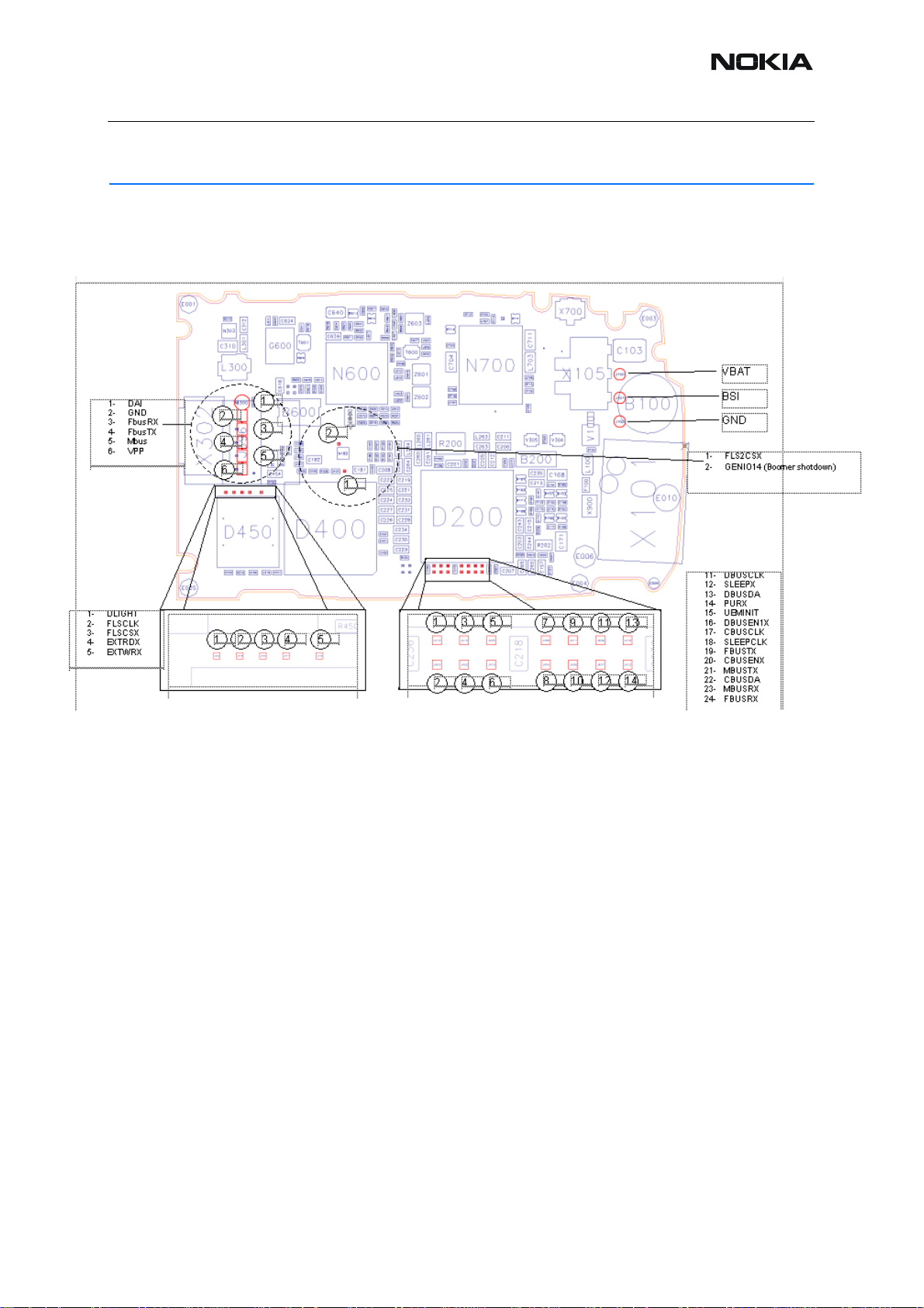
Baseband Troubleshooting
■ Baseband test points
Figure 1:BB test points
Nokia Customer Care
ISSUE 1 09/2004 COMPANY CONFIDENTIAL 7
Copyright © 2004 Nokia. All Rights Reserved.
Page 8
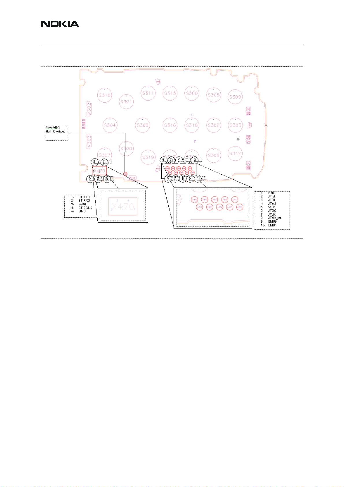
Nokia Customer Care
RH-53/54
Figure 2:BB test points 2
■ Tr oubleshooting diagrams
INOTE : Since both D200 (UEM) and D400(UPP) are underfilled, they can not be replaced. If
either D200 or D400 is defective, the whole PWB has to be discarded.
8 COMPANY CONFIDENTIAL ISSUE 1 09/2004
Copyright © 2004 Nokia. All Rights Reserved.
Page 9
RH-53/54
Nokia Customer Care
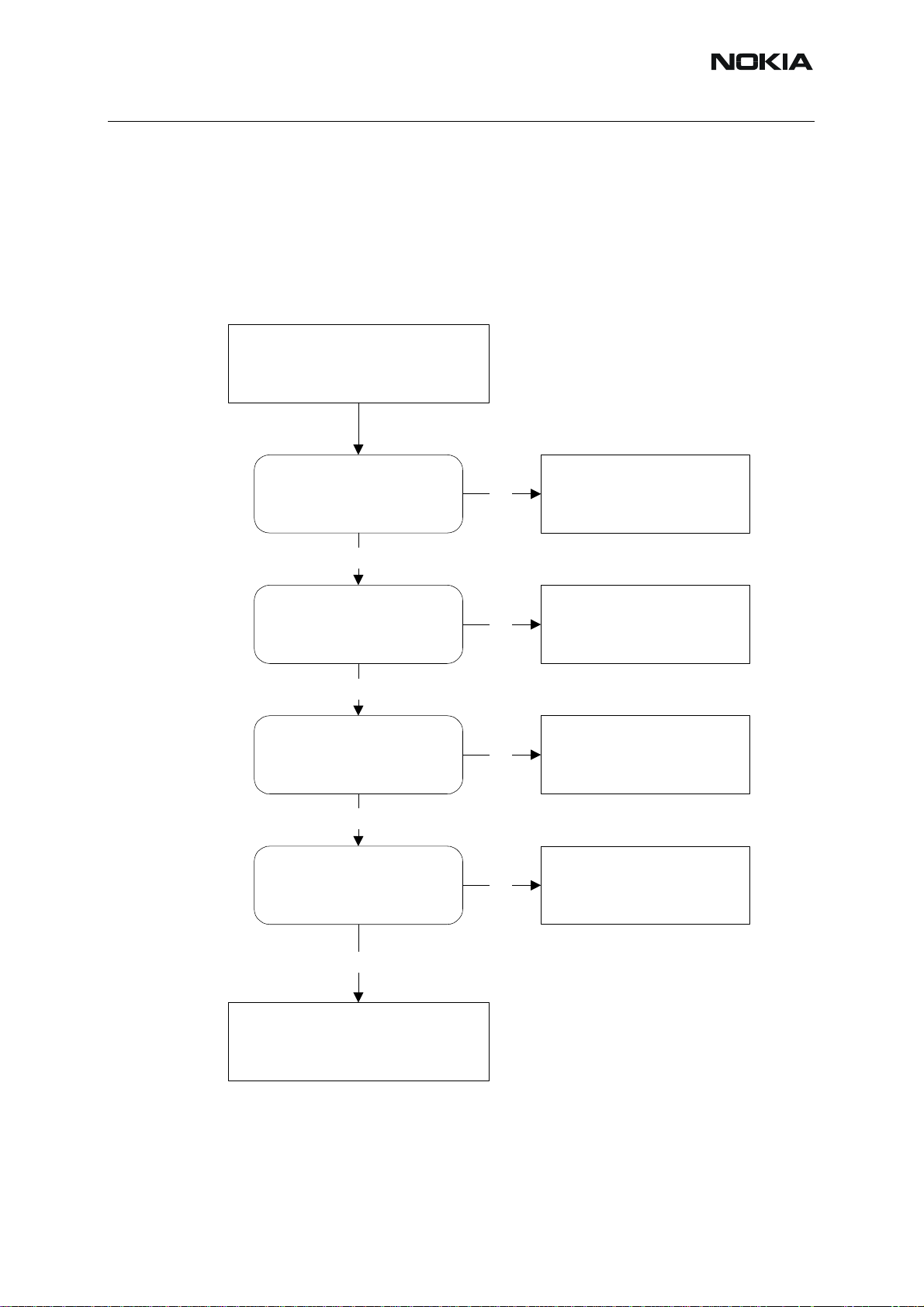
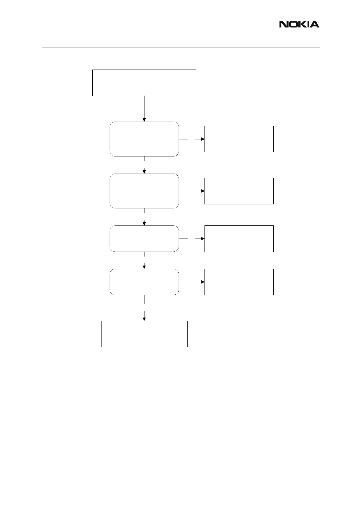
■ Phone is dead
This means that the phone do not draw any current at all when supply is connected and/or
powerkey is pressed.
It is assumed that the voltage supplied is 3.6 VDC. The UEM will pre vent any functionality what
so ever at battery/supply levels below 2.9 VDC.
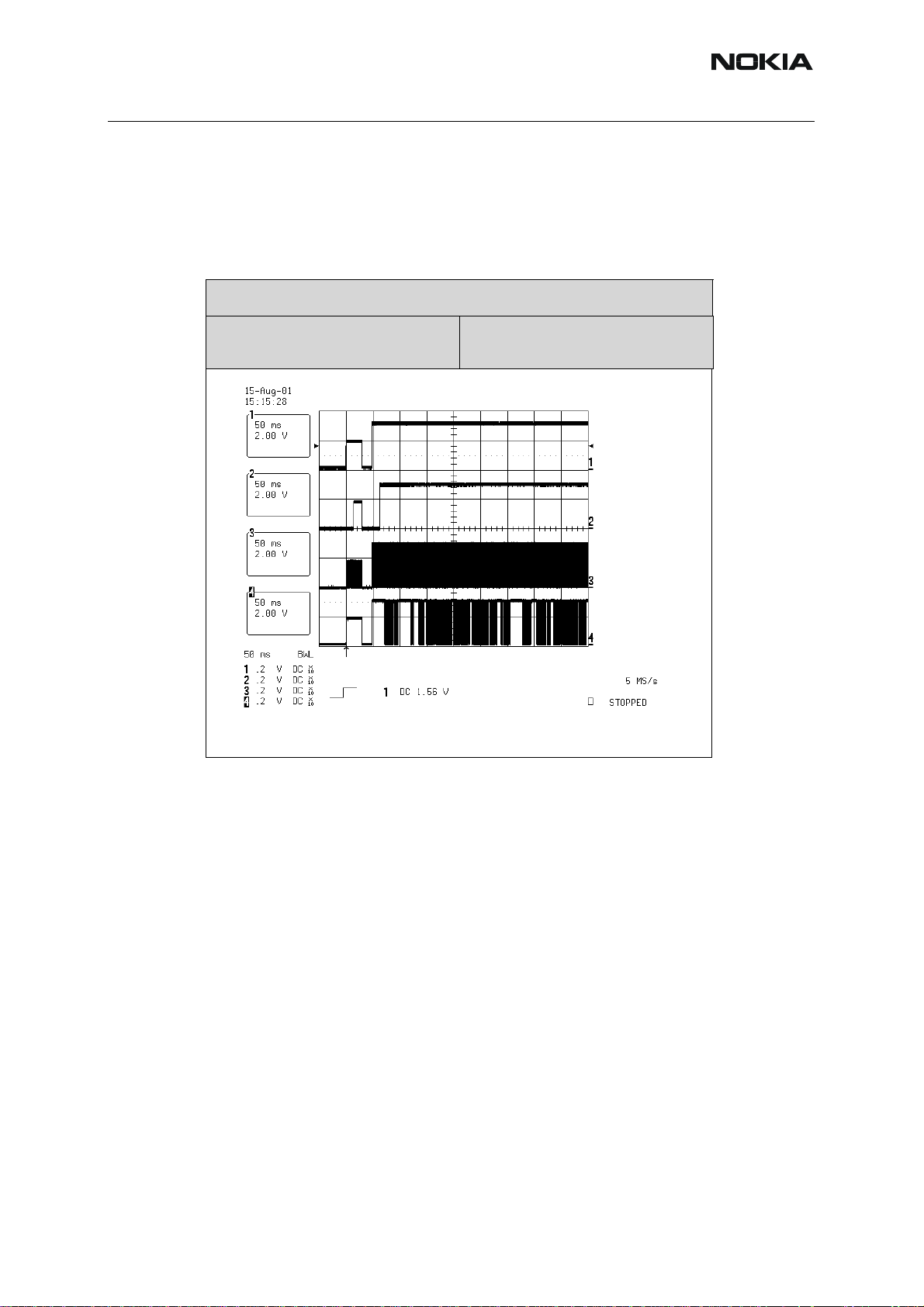
Figure 3:Phone is dead troubleshooting
Phone is dead
Yes
X105
VBAT = 3,6VDC
Yes
C103
L260,L261,L262,L263,L264,L265
C260,C261,C262,C263,C264,C265
Voltage = 3,6VDC
Yes
J404
Sleep-clock is
32.768 kHz, 1,8Vpp
Yes
J402
PURX = 1,8VDC,
1 sec. after power-key
is pressed
Yes
C227
VR3 = 2,78VDC
No
No
No
No
No
Check :
X105
Check :
C103
L260,L261,L262,L263,L264,L265
C260,C261,C262,C263,C264,C265
Check :
B200, C209, C210, PW B. Else
defective D200*
Check :
PWB.
Else defective D200*
Check :
C227, PWB.
Else defective D200*
Yes
26 MHz clock min. 300mVACpp,
R426
probe Cin=10-13 pF/10M
Yes
No
Check :
C227, C420, R420, PWB.
Else defective D200*
Check :
D450 (Flash).
Else defective D200*
ISSUE 1 09/2004 COMPANY CONFIDENTIAL 9
Copyright © 2004 Nokia. All Rights Reserved.
Page 10
RH-53/54
Nokia Customer Care
■ Flash programming does not work
The flash programming can only be done via the pads on the PWB (J396).
In case of Flash failure in FLALI station, problem is most likely related to SMD problems. Pos-
sible failures could be short-circuit of balls under µBGAs (UEM, UPP, FLASH). Missing or misaligned components.
In flash programming error cases the flash prommer can give some information about a fault.
The fault information messages could be:
- Phone doesn't set FBUS_TX line low
Because of the use of uBGA components it is not possible to verify if there is a short circu it in
control- and address lines of MCU (UPP) and memory (flash).
Figure 4:Flash programming troubleshooting
Flash prgramming
do not work
Error fro m p ro mmer:
"Phone doesn't set
FBUS_T X line low"
Yes
J396, R108
Check connection between
pad 1,2 & 3 on J396
and R108
Yes
J409, J410, J411, J412
Voltage level at 1,8VDC
Yes
Try re a d in g MCU ID
with Phoenix.
Reading OK?
Yes
Try reading Flash ID
with Phoenix.
Reading OK?
No
No
No
No
Check :
R108, PW B
Check :
PWB.
Else defective D200*
Check :
PWB.
Else defictive D400*
Check :
Replace D450
Yes
Reflash phone
10 COMPANY CONFIDENTIAL ISSUE 1 09/2004
Copyright © 2004 Nokia. All Rights Reserved.
Page 11
RH-53/54
Nokia Customer Care
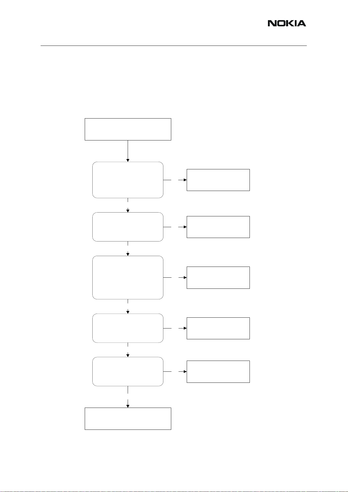
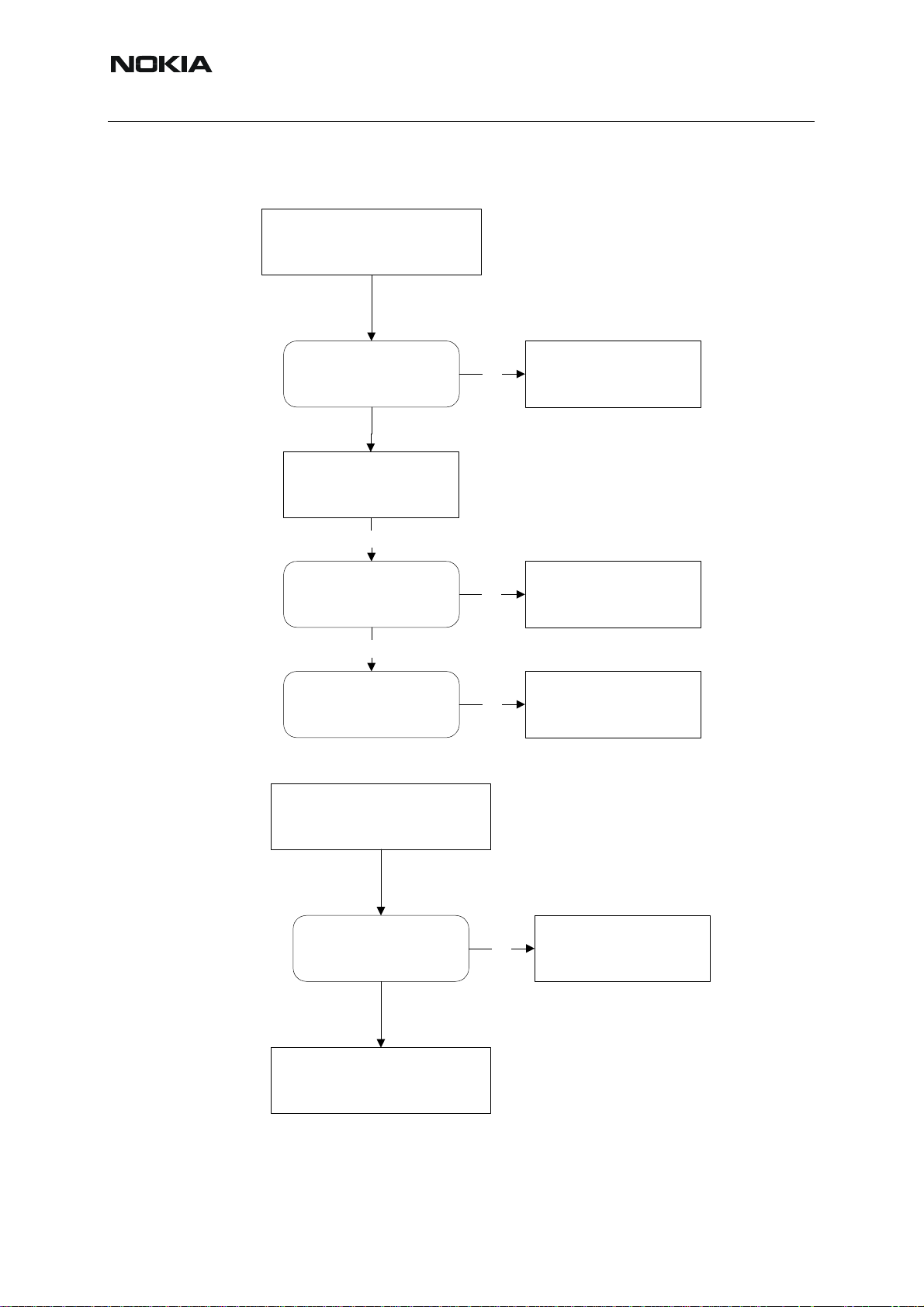
■ Power does not stay on or phone is jammed
If this kind of failure is presenting itself immediately after FLALI, it is most likely caused by
ASICs missing contact with PWB.
If for some reason the MCU does not service the watchdog register within the UEM, the operations watchdog will run out after approximately 32 seconds. Unfortunately , the service routine
can not be measured.
Figure 5:Phone jammed troubleshooting
Power doesn't stay on,
or phone is jammed
J404
Sleep clock = 32.768 kHz,
1.8Vpp
Yes
J402
PURX = 1,8VDC,
1 sec. after power-key i s
pressed
Yes
UI functionality,
and keys react
to pressure?
Yes
R426
26 MHz clock min.
300mVACpp,
probe Cin=10-13 pF/10M
No
No
No
No
Check :
B200, C209, C210, PW B.
Else defective D200*
Check :
PWB.
Else defictive D200*
Check :
D450, Keymat,
Lightguide, PWB .
Else defective D400*
Check :
C420, C426, R420,
R426, N600(Mjoelner)
Yes
Reflash phone
ISSUE 1 09/2004 COMPANY CONFIDENTIAL 11
Copyright © 2004 Nokia. All Rights Reserved.
Page 12
RH-53/54
Nokia Customer Care
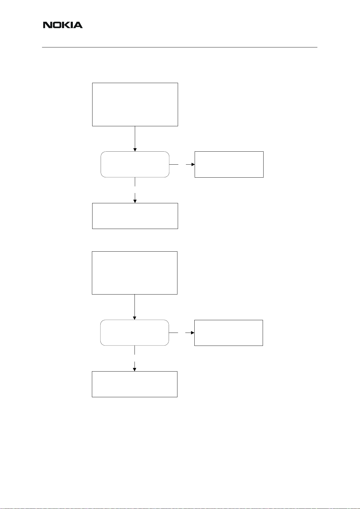
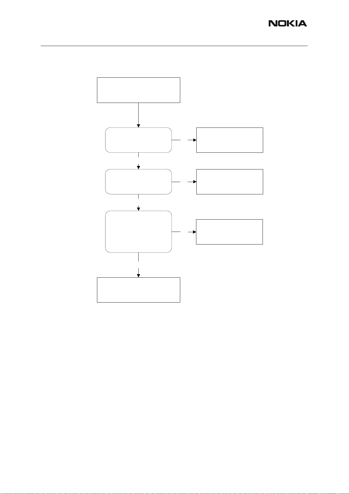
■ Display information : "Contact Service"
This error can only happen at power up where several self-tests is run. If any of these test cases
fails the display will show the message: "Contact Service".
It's individual test cases so the below lineup of error hunting's has no chronological order . Use
common sense and experience to decide which test case to start error hunting at.
Figure 6:Troubleshooting when Contact Service message seen
Display shows
"Contact Service"
Yes
EarDa & MicDa
between
UPP and UEM?
MBUS interface
between
UPP and UEM?
AuxDa & UEMInt
between
UPP and UEM?
SleepX & SleepClk
between UPP & UEM?
TXI/QD & RXI/QD?
SIM interface between
UPP & UEM
No
Check :
PWB.
Else defective D200*
or D400*
Key is stucked
Flash checksum
y ASIC version vs. compilation flag, PMM checksum
y PMM validity
y Warrenty Information State
y SIM-Lock
Check :
A-face, domesheet, PWB.
Reflash phone
Check :
PWB.
Else defective D450 (FLASH)
12 COMPANY CONFIDENTIAL ISSUE 1 09/2004
Copyright © 2004 Nokia. All Rights Reserved.
Page 13
RH-53/54
Nokia Customer Care
■ The phone does not register to the network, or the phone cannot make a call
If the phone doesn't register to the network, the fault can be in either BB or RF . Only few signals
can be tested since several signals is 'burried' in one or more of the inner layers of the PWB.
First of all check that SIM LOCK is not causing the error by using a Test-SIM card and connect
the phone to a tester.
Figure 7:No call troubleshooting
Phone do not register to
network
or phone cannot make a call
C222, C223, C224, C225,
C226, C227
Voltage = ~2,78VDC
All during GSM frame-
call mode.
Use TXP on C646 as trigger
Yes
C230, C231
Voltage = ~1,35VDC
All during GSM frame (call mode)
Use TXP on C646 as trigger
Yes
J421, J422, J423
Check RF serial bus during
GSM-frame :
Logic HIGH = 1,8VDC
Logic LOW = 0V DC
RFBUSC LK (J421),
RFBUSD A (J422),
RFBUSEN1X (J423)
Yes
R601, R603
Check analog signals during
GSM-frame (RX slot):
RXIP/N (R601) = 0-1,45VDC
RXQP/N (R603) = 0-1,45VDC
Check :
No
C222,C223, C224, C225,
C226, C 227 , P WB .
Else defective D200 or D400*
Check :
No
C230, C 231 , P WB .
Else defective
D200* or D400*
Check :
No
Else defective D200*
Check :
No
Else defective D200*
PWB.
or D400*
PWB.
or D400*
Yes
R610, R611
Check analog signals during
GSM-frame (TX slot):
TXIP/N (R610) = 1-1,75VDC
TXQP/N (R611) = 1-1,75VDC
Yes
No
Check :
R610, R 611 ,P WB .
Else defective D200*
or D400*
Check RF
ISSUE 1 09/2004 COMPANY CONFIDENTIAL 13
Copyright © 2004 Nokia. All Rights Reserved.
Page 14
Nokia Customer Care
■ Charging troubleshooting
Figure 8:Phone is OFF:no current from charger
Phone is OFF - battery is
completely empty
(<=3,1VDC)
and no current from
charger when connected
RH-53/54
L100
VCHAR > 2,1VDC
Yes
Defective D200*
Phone is ON or OFF - battery
nominal voltage (~3,6VDC)
and no current from
charger when connected
L100
VCHAR > 3,6VDC
No
No
Check :
F100, L100, V100, C100,
R200, System-connector.
Check :
F100, L100, V100, C100,
R200, System-connector.
Yes
Defective
D200 or D400*
14 COMPANY CONFIDENTIAL ISSUE 1 09/2004
Copyright © 2004 Nokia. All Rights Reserved.
Page 15
RH-53/54
Nokia Customer Care
Figure 9:Display info:charger connected, not charging
Display info when
charger is connected :
"Not charging"
R206
Voltage on R206 towards
D200 is ~0,8VDC
when power is connected.
Yes
R207
Voltage (use scope) on R207
towards D200 is ~0,9VDC at
peak.
No
No
Check :
X105, R202, R206, C240.
Check :
X105, R202, R207, C220.
Yes
R200
Voltage on R200 towards
D200 same as VBAT voltage
Yes
R200
Voltage rises slowly on
R200 towards D200 when
charger is connected.
Yes
Check :
PWB
No
No
Check :
R200, PWB.
Else defective D200*v
Check :
PWB.
Else defective D200*
ISSUE 1 09/2004 COMPANY CONFIDENTIAL 15
Copyright © 2004 Nokia. All Rights Reserved.
Page 16
Nokia Customer Care
■ Audio troubleshooting 1, 2
Figure 10:Microphone does not work
Microphone do not work and
the isn't any mechanical
problem
RH-53/54
Z100
Check Z100 is
working correctly
(no short/open-circuit)
No
Replace :
Mic and micboot
Error still present
R165
Check voltage level on
R165 towards UEM (bias)
= 2,1V
Yes
No
R165, C168, PWB.
Else defctive D200*
R153
Check voltage level on
R153 towards mic-lines (bias)
= 1,0V - 1,4V
No
R153, R157,C151, C152,
C153, C154,R171, PWB.
Figure 11:Top: Earpiece does not work
Headset earpiece do not
work and the isn't any
mechanical problem
Replace :
Z100
Check :
Check :
R183, Z102
Check R183, Z102 is
working correctly
(no open-circuit)
No
Replace :
C183 and/or Z102
Defective D200*
16 COMPANY CONFIDENTIAL ISSUE 1 09/2004
Copyright © 2004 Nokia. All Rights Reserved.
Page 17
RH-53/54
■ Audio troubleshooting 3: Headset does not work
Figure 12:Headset does not work
Headset microphone do not
work and the isn't any
mechanical problem
Nokia Customer Care
Z101
Check Z101 is working
correctly
(No short/open circuit)
Yes
R151
Check voltage level on R151
towards UEM (bias)
= 1,0V - 1,4V
Yes
R151
Check voltage level on R151
towards UEM (bias) = 1,0V -
1,4V
Check XMIC line to UEM
(D200)
Error still present
Defective D200*
No
No
No
Replace :
Z101
Check :
R166, R151, C171
Check :
R156, C170, C174, C172,
R169
ISSUE 1 09/2004 COMPANY CONFIDENTIAL 17
Copyright © 2004 Nokia. All Rights Reserved.
Page 18
RH-53/54
Nokia Customer Care
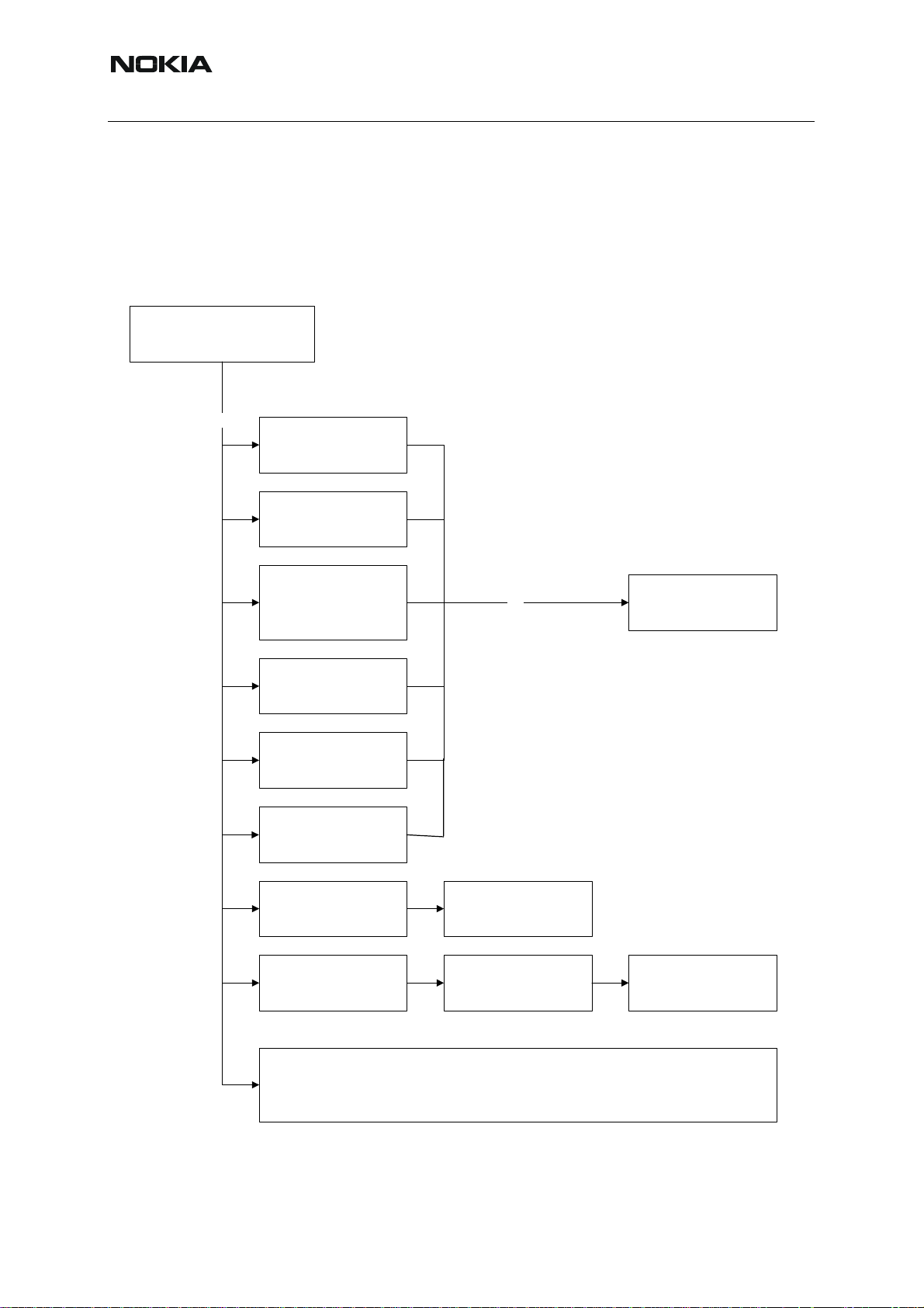
Upper block failures
All checks can be done while the phone is partially disamsembled (no need for full reasembly
inbetween debugging steps):
SIM failure (including insert SIM faults)
1. Flex B2B connector pressed in?
2. Change LCD can assembly (for new flex) works?
3. C314 (VSIM cap) short circuitting?
4. C313 (SIMIO cap) short circuitting?
5. Voltages (SIM startup sequence)? Board to Board connector pin17
6. Change main PWB (UEM)?
The hardware of the SIM interface from UEM (D200) to the SIM co nnector can be teste d wit hout a SIM card. When the power is switched on the phone first check for a 1,8V SIM card and
then a 3V SIM card. The phone will try this four times, whereafter it will display ”Insert SIM
card”.
VSIM – Board to board connector pin 17
Reset – Board to board connector pin 29
Clock – Board to board connector pin 20
Data – Board to board connector pin 19
Check for SIM voltage during power-up
Ch1 : VSIM
Ch2 : RESET
Ch3 : CLOCK
Ch4 : DATA
18 COMPANY CONFIDENTIAL ISSUE 1 09/2004
Copyright © 2004 Nokia. All Rights Reserved.
Page 19
RH-53/54
Nokia Customer Care
The error ”SIM card rejected” means that the A TR message received from SIM card is corrupted, e.g. data signal levels are wrong. The first data is always ATR and it is sent from card to
phone.
For reference a picture with normal SIM power-up is shown below.
Normal SIM power-up sequence
Ch1 : VSIM
Ch2 : RESET
Ch3 : CLOCK
Ch4 : DATA
Vibra failure
1. Flex B2B connector pressed in?
2. Change C2 cover assembly(new vibra)/Vibra works?
3. Change LCD can assembly (new flex) works?
4. Change main PWB (UEM)?
ISSUE 1 09/2004 COMPANY CONFIDENTIAL 19
Copyright © 2004 Nokia. All Rights Reserved.
Page 20
Nokia Customer Care
Figure 13:Vibra troubleshooting
Start
Wrong setting or
software error.
Contact problem.
Mechanical problem
Is there any
vibration?
Yes
No
- counterweight is
blocked
Defective o r missing
vibra.
Defective UEM.
RH-53/54
Is there
sufficient
vibration?
Yes
Vibra is
constantly
switched
on?
No
Intermittent
vibration?
No
Acoustical
noise?
No
Yes
Yes
Software error
Contact problem.
Defective vibra.
Defective UEM.
Software error.
Defective UEM.
Short circuit.
Yes
Bad connection.
Defective vibra.
Defective vibra.
Mechanical problem
- counterweight hits
LCD can/C2 cover
Loose parts in
phone.
Speaker failure
1. Flex B2B connector pressed in?
20 COMPANY CONFIDENTIAL ISSUE 1 09/2004
Copyright © 2004 Nokia. All Rights Reserved.
Page 21

RH-53/54
Display failure
Nokia Customer Care
2. C2 cover mounted correct (red snap not vissible)?
3. Check if system connector is misplaced slightly?
4. Check for ”headset inserted symbol” in display?
5. Change speaker chamber/antenna works?
6. Change LCD can assembly (for new flex) works?
7. Change main PWB (UEM)?
1. Flex B2B connector pressed in?
2. Display B2B connector pressed in (press through hole in C2 cover assembly)?
3. Change display works?
4. Change LCD can assembly (for new flex) works?
5. R316 (LCDRESETX) missing?
Fold detection failure
1: Check if magnet is mounted on bottom side of C2 cover assembly
(with a spare screw)
2: Check if N306 (Hall IC) is mounted?
Note:
Don’t try and rework flex!! Handling is likely to cause the solder pads to brake or disconncect
from track, which cannot be repaired in a reliable wa y by resoldering. Only reliable repair option
is to change the flex (LCD can assembly)!
ISSUE 1 09/2004 COMPANY CONFIDENTIAL 21
Copyright © 2004 Nokia. All Rights Reserved.
Page 22

Nokia Customer Care
RH-53/54
[This page intentionally left blank]
22 COMPANY CONFIDENTIAL ISSUE 1 09/2004
Copyright © 2004 Nokia. All Rights Reserved.
Page 23

RH-53/54
Nokia Customer Care
Introduction to RH-53/54 RF Troubleshooting
Three types of measurements are used in the following. It will be specified if the measurement
type is "RF" “RF test” or "LF".
• RF measurements should be done with a GSM tester and a suitable connector to
the general RF input/output. That connection is for tun ing a nd te sting the whole RF
in the phone.
• RF test measurements should be done with a Spectrum Analyzer and a high-frequency 500ohm passive probe, for example HP54006A. Use some sort of DC blocking device, to avoid loading the circuit or the SPA with DC. (Note that when
measuring with the 500ohm probe, the signal will be around 20 dB attenuated. The
values in the following will have these 20 dB subtracted and represent the real value
seen on the spectrum analyzer).
• LF (Low frequency) and DC measurements should be done with a 10:1 probe and
an oscilloscope. The probe used in the following is 10MΩ/8pF passive probe . If using another probe then bear in mind that the voltages displayed may be slightly different.
Always make sure the measurement set-up is calibrated when measuring RF parameters on
the antenna connector. Remember to in clude the loss in the module rep air jig and the coaxial
cable when realigning the phone.
Most RF semiconductors are static discharge sensitive. So ESD prot ection must be taken
during repair (ground straps an d ESD soldering irons). Mjoelner is mo isture sensitive so parts
must be pre-baked prior to soldering.
Apart from key-components described in this document there are a lot of discrete components
(resistors, inductors and capacitors) for which troubleshooting is done by checking if soldering
of the component is done properly or checking if the component is missing from PCB. Capacitors can be checked for short-circuit and resistors for value by means of an ohmmeter, but be
aware in-circuit measurements should be evaluated carefully.
In the following both the name “low band” will be used to describe both GSM850 - EGSM and
GSM900, while “high band” will be used for both PCN and GSM1800.
ISSUE 1 09/2004 COMPANY CONFIDENTIAL 23
Copyright © 2004 Nokia. All Rights Reserved.
Page 24

RH-53/54
Nokia Customer Care
General description of the RF circuits
In the following general desriptions different colours are used in the block diagram. The Lowband signal route is shown in red, the Highband route in green and the common signal lines
are shown in blue.
■ Receiver signal path
The signal from the antenna pad is routed to the Front End Module (FEM - N700). The FEM
contains a diplexer and a switch system controlling the direction of the signals, either routing
the TX signal from the Power Amplifier (P A) to the anten na or routing the received signal from
the antenna to either the Lowband (850/900 MHz) or the Highband (1800/1900 MHz) input on
the RF IC (N600).
Figure 14:Receiver signal path
Rx
Ant
Diplexer
RX/TX switch
PA and detector
GSM RX
PCS RX
supply
F
X
R
D
D
V
LNA
Bias
INMH
INPL
INML
INPM
INMM
INPH
ASIC
LNA
LNA
LNA
Pre-gain
Pre-gain
SAW
RX850/
900
SAW
RX1800/
1900
filter
222
2
1/2 1/4
Mjølner
BBAMP
BBAMP
B
B
X
R
D
D
V
BIQUAD
DCN1
LPF1
DCN1
LPF1
AGC
AGC
LPF2
BIQUAD
LPF2
DCN2
DCN2
VRX
RXIP
RXIM
RXQP
RXQM
VR6
1/4
1/2
The Lowband signal from the FEM is routed to the SAW filter (Z602). The purpose of the SA W
filter is to provide out-of band blocking imummity and to provide the LNA in Mjoelner (N600)
with a balanced signal. The front end of Mjoelner is divided into a LNA and Pre-Gain amplifier
before the mixers.
The output from the mixer is fed to Baseband part of Mjoelner where the signals amplified in
the BBAMP aand low pass filteret in LPF1 before the DC compensation circuits in DCN1. The
DCN1 output is followed by a controlled attenuator and a se cond lowp ass filter LPF2. The ou tput from LPF2 is DC centeret in DCN2 before being feed to the BB for demodulation.
The Highband signal chain is similar to the lowband.
■ Transmitter signal path
The I/Q signal from the BB is routed two the modulators for both Lowband and Highband. The
output of the modulators is either terminated in a SA W filte r (Z603) for the Lowb and or a balun
for the Highband. The signals from the SAW and Balun are then amplified in the Power Amplifier (PA) located in the Front End Module (FEM - N700) where the gain control t akes place. In
24 COMPANY CONFIDENTIAL ISSUE 1 09/2004
Copyright © 2004 Nokia. All Rights Reserved.
Page 25

RH-53/54
Nokia Customer Care
order to control the TX level a sample of the signal is taken in the FEM and used in the power
loop amplfier in Mjoelner to establish the right output power. The selection of which amplifier
chain in the FEM to be active is controlled through the 4 controllines VC1, VC2, BS and Vtx.
Figure 15:Transmitter signal path
Ant
Diplexer
RX/TX switch
PA and detector
Vapc
Vsense
VC1 (TX/RX GSM)
VC2 (TX/RX DCS)
VTX
Band sel
PCN/PCS
GSM
PCN/PCS
Balun
VTX
SAW
PW-loop
filter
VPCTRL_G
VANTL
VANTM
VANTH
VB_DET
VTXLOL
VTXLOH
VTXBH
VTXBL
OUTHP
OUTHM
OUTLP
OUTLM
DET
PLFB1
PLFB2
ASIC
RF Controls
RF Controls
Open collector
Open collector
VDDDIG
VDDRXBB
PWC
TXP
Mjølner
1/2
1/2
2
TXC
VDDTX
Supply
filter
1/4
1/4
2
2
2
2
2
VTX
TXQP/TXQM
VBATTRF
VR2
TXC
TXP
TXIP/TXIM
■ PLL
The PLL supplies Local Oscillator (LO) signals for the RX and TX-mixers. In order to be able
to generate LO-frequencies for the required EGSM and PCN channels a regular synthesizercircuit is used. All blocks for the PLL except for the VCO, reference X-tal and loopfilter is lo cated
in the Mjoelner IC, N600.
The reference frequency is generated by a 26MHz V olt age Controlled X-tal Oscillator (VCXO)
located in the Mjoelner IC. Only the X-tal is external. 26MHz is supplied to BB where a divideby-2 circuit (located in the UPP IC) generates the BB-clock at 13MHz. The reference frequency
ISSUE 1 09/2004 COMPANY CONFIDENTIAL 25
Copyright © 2004 Nokia. All Rights Reserved.
Page 26

RH-53/54
Nokia Customer Care
is supplied to the reference divider (RDIV) where the frequency is divided by 65. The output of
RDIV (400kHz) is used as reference clock for the Phase Detector (ϕ).
The PLL synthesizer is a feedback control system controlling the phase and frequency of the
LO-signal. Building blocks for the PLL are: Phase detector, Charge Pump, Voltage Controlled
Oscillator (VCO), N-Divider and loopfilter. As mentioned earlier only the VCO and loopfilter is
external to the Mjoelner IC.
The VCO (G600) is the component that actually generates the LO-frequency. Based on the
control voltage input the VCO generates a signal, which is made differential through a balun.
This signal is fed to the Prescaler and N-divider in Mjoelner, these 2 block together divide the
frequency by a ratio based on the selected channel. The divider output is supplied to the phase
detector which compares the frequency and phase to the 400kHz reference clock. Based on
this comparison the phase detector controls the charge pump to either charge or discharge the
capacitors in the loopfilter . By charging/discharging the loop filter the control voltage to the VCO
changes and the LO-frequency will change. Therefore the PLL will make the LO-frequency stay
locked to the 26MHz VCXO frequency.
The loopfilter consists of the following components: C639-C641 and R618-R619.
The PLL is operating at twice the channel center frequency when transmitting or receiving in
the PCN band. For the EGSM band the PLL is operating at 4-times the channel frequency.
Therefore divide-by-2 and divide-by-4 circuits are inserted between the PLL output and LO-inputs to the PCN and EGSM mixers.
The frequency plan is shown in the figure below:
Table 1: Frequency table
Frequency
Band
GSM
850
EGSM
900
GSM
1800
Channel #
RX 128 – 251 869.2 – 893.8 3476.8 – 3575.2
TX 824.2 – 848.8 3296.8 – 3395.2
RX 975 – 1023
1 – 124
TX 880.2 – 914.8 3520.8 – 3659.2
RX 512 – 885 1805.2 – 1879.8 3610.4 – 3759.6
TX 1710.2 – 1784.8 3420.4 – 3569.6
System Frequency Band
[MHz]
925.2 – 959.8 3700.8 – 3839.2
PLL Frequency Band
[MHz]
PCN RX 512 – 810 1930.2 – 1989.8 3860.4 – 3979.6
TX 1850.2 – 1909.8 3700.4 – 3819.6
According to the figures above the PLL must be able to cover the f requency range 3420.4MHz
to 3839.2MHz for the GSM900/1800 and 3296.8 to 3979.6MHz for the GSM850/1900.
26 COMPANY CONFIDENTIAL ISSUE 1 09/2004
Copyright © 2004 Nokia. All Rights Reserved.
Page 27

RH-53/54
To PCN RX
mixer
ASIC
2 22
2
To GSM RX
mixer
Nokia Customer Care
Figure 16:Frequency plan
1/2
1/2
222
2
To PCN
Modulator
Mjoelner
N600
1/4
1/4
To GSM
Modulator
VDDRXBB
Resistor Ext/R2H/R2
VBEXT
Ref.
filte
r
1
VREF
RFCONV_0(9)
Main Bias
Circuit
VDDLO
VDDPLL
VDDPRE
Buffer
VDDCP
CPOUT
VDDXO
VDDBBB
REFOUT
XTALM
XTALP
INPLO
INMLO
VDDDIG
VDDDL
SELADDR
RESETX
RF_EN
RF_CLK
RF_DATA
RESETX
VCOSENSE
3
Charge
Pump
Lock
Detect
1/2
level
shift
I/O
64/
65
RBEXT
2,7k
LOCNT
REFCNT
NDIV
ADIV
VCXO Bias
VDDRXBB
SENSE
Rpa
PA vendor
indication
33k : Hitachi
82k : RFMD
RDIV
R2H/R2
VDDTX
Sensor
BIST / Temp.
ϕ
AFC/CAL
Control
Buf/
AGC
Digital
Control
Synth
supply
filter
Vcp
supply
filter
PLL
loop
filter
VCXO
supply
filter
26MH
z
3
VPLL
VXO
REFOUT
VVCO
VBB (1.8V)
Ref clk set
RESET_X_M
RFBUSX
RFBUSDA
RFBUSCLK
VR5
VR3
VR7
VR2
VIO
VIO
GENIO6
ISSUE 1 09/2004 COMPANY CONFIDENTIAL 27
Copyright © 2004 Nokia. All Rights Reserved.
Page 28

Nokia Customer Care
■ RF Key component placement
Figure 17:RF key component placement
RH-53/54
Table 2: Key component placement tABLE
N600 Mjoelner RF IC
Z601 PCN RX SAW High band RX SAW filter
Z602 EGSM RX SAW Low band RX SAW filter
Z603 EGSM TX SAW Low band TX SAW filter
B600 26 MHz crystal
G600 VCO ( 3.6 GHZ VCO )
N700 Front End Module (FEM)
X700 RF connector
28 COMPANY CONFIDENTIAL ISSUE 1 09/2004
Copyright © 2004 Nokia. All Rights Reserved.
Page 29

RH-53/54
Nokia Customer Care
Troubleshooting
■ Common circuit
The power supply and the synthesiser is common for RH53/54, except for the synthesiser ranges.
Power Supply Configuration
All power supplies for the RF Unit are generated in the UEM IC (D200). All power outputs from
this IC have a decoupling capacitor at which the supply voltage can be checked.
The power supply configuration used in the phone is shown in the block diagram below:
Figure 18:Power supply configuration
Internal Mjoelner
VR2
2.78 v +/-3%
@100 mA
TX modulator
VR3
VR5
UEM
VR1a
VrefRF01
VR6
VIO
VR7
Modulator loading
netwok
2.78 V +/-3%
@20 mA
2.78 V +/-3%
@50 mA
4.75 V +/-3%
@10 mA
1.35 V +/- 2%
< 100 uA
2.78 V +/-3%
@50 mA
1.8 V +/- 4.5%
@150 mA
2.78 V +/- 3%
@45 mA
Power Loop Amp
Digital control logic
VCXO Power Supply
Baseband clk buffer
Dividers & LO buffer
PLL Pre-scaler
PLL Counters
PLL charge pump
Ref. volt for Mjoelner
LNA and Pre-gain
BB Section
Digital com. interface
VCO module
VCO
VR4
Vbat
2.78 V+/- 3%
@50 mA
Not used
Front End Module
ISSUE 1 09/2004 COMPANY CONFIDENTIAL 29
Copyright © 2004 Nokia. All Rights Reserved.
Page 30

Nokia Customer Care
The names to the left are the signal names used on the RF schematics
Table 3: Supply names
RH-53/54
Supply
name RF
Supply
name UEM
Min Typ Max Unit
VCP VR1A 4.54 4.75 4.9 V
VTX VR2 2.64 2.78 2.86 V
VXO VR3 2.64 2.78 2.86 V
VPLL VR5 2.64 2.78 2.86 V
VRX VR6 2.64 2.78 2.86 V
VVCO VR7 2.64 2.78 2.86 V
VBB VIO 1.72 1.8 1.88 V
VREF2 VrefRF01 1.334 1.35 1.366 V
VBATT BATTERY 3.1 3.6 5.2 V
See the picture below for measuring points at the UEM (D200).
Figure 19: UEM measuring points
VR2=VTX (C223)
VR6=VRX (C225) VR1A=VCP (C221)
VR7=VVCO (C224)
VR3=VXO (C227)
VR5=VPLL (C226)
VrefRF01=VREF1 (C231)
VIO=VBB (C218)
There is only one PLL synthesizer generating Local Oscillator frequencies for both RX and TX
in both bands (Lowband and Highband). The VCO frequency is divided by 2 for Highband operation or by 4 for Lowband operation inside the Mjoelner IC.
30 COMPANY CONFIDENTIAL ISSUE 1 09/2004
Copyright © 2004 Nokia. All Rights Reserved.
Page 31

RH-53/54
Nokia Customer Care
■ General instructions for Synthesizer troubleshooting
Start the Phoenix-Service-Software and
Select:ProductRH53/54 or scan
Select:Testing
RF Controls
Band XX, se table below
Active UnitRX
Operation ModeContinuous
RX/TX ChannelYY se table below
The signal from the VCO is measured at R640 using a spectrum analysator and a 500ohm p assive probe. The frequency should be as found in the table below and the power should be
around –20dBm.
Table 4: Frequency table
ZZ XX YY PLL frequency [MHz]
RH-54 GSM850 189 3525.6
RH-53 GSM900 36 3768.8
RH-53 GSM1800 700 3685.6
RH-54 GSM1900 661 3920
■ 26 MHz Reference Oscillator ( VCXO )
The 26 MHz oscillator is located in the Mjoelner IC (N600). The coarse frequency for this oscillator is set by an external crystal (B600). The reference oscillator is used as a reference frequency for the PLL synthesizer and as the system clock for BaseBand. The 26MHz signal is
divided by 2 to achieve 13MHz inside the UPP IC (D400). The 26 MHz signal from the VCXO
can be measured by probing R420 at the end towards the UPP, see “Measurement points for
the Synthesizer”. The level at this point is approx. 700mVpp. Frequency of this oscillator is adjusted by changing the AFC-register inside the Mjoelner IC. This is done via the Mjoelner serial
interface.
ISSUE 1 09/2004 COMPANY CONFIDENTIAL 31
Copyright © 2004 Nokia. All Rights Reserved.
Page 32

Nokia Customer Care
Example Signal Measured at VCXO output (R420)
Figure 20:Measured signal at VCXO output
RH-53/54
VCO
The VCO is generating frequencies in the range of 3420.4MHz – 3839.2 MHz for the RH-53
and in the range 3296.8 to 3979.6 MHz for RH-54 when the PLL is running. The output frequency from the VCO is led to the Local oscillator input of the Mjoelner IC (N600), where the frequency is divided either by 2 or 4 in order to generate all channels in EGSM and PCN
respectively . Frequency of the VCO is controlled by a DC-volt age (Vctrl) coming from the loopfilter. The loopfilter consists of the component s R618, R619 and C639-C641. Range of the Vctrl
when the PLL is running (locked) is 0.4V – 4.3V. Even if the PLL is not in locked state (Vctrl
out of range) there is some frequency at the output of the VCO (G600), which is between 3 and
4 GHz. This is true if the VCO is working and if the VCO power supply is at present (2.7V).
32 COMPANY CONFIDENTIAL ISSUE 1 09/2004
Copyright © 2004 Nokia. All Rights Reserved.
Page 33

RH-53/54
■ Tr oubleshooting chart for the Synthesizer
Figure 21:Troubleshooting chart for synthesizer
From Phoenix chose:
File > product > RH-53/54
Maintenance > Testing > RF controls > band > RX >
continous > channel
Band and channel according to the previous table
Nokia Customer Care
Spectrum analyser
VCO frequency (R640)
MHz (see table)
No
Osciloskope
VXO Power supply
(C618)
2.78Vdc
Yes
Osciloskope
VXO Power supply
(C620)
2.78Vdc
Yes
Osciloskope
VCXO output
(R420) 26MHz
approx. 700mVpp
Yes
Yes
No
No
No
PLL block functional
Check UEM, SW
Phone not in function
Check R605, SW
Phone not in function
VCXO is not functional
Check crystal (B600)
Osciloskope
PLL Power supply
(C614, C634)
All 2.7Vdc
No
Check UEM, SW
Phone not in function
Yes
Osciloskope
PLL Charge pump
supply
(C616)
All 4.75Vdc
No
Check R603, C645, UEM,
SW
Phone not in function
N600 not functional
Yes
Spectrum analyser
VCO output (R640)
some signal between
3 and 4 GHz
No
VCO (G600) is not functional
Check Loop filter (R618,
R619, C639-C641)
YES
ISSUE 1 09/2004 COMPANY CONFIDENTIAL 33
Copyright © 2004 Nokia. All Rights Reserved.
Page 34

RH-53/54
Nokia Customer Care
If the phone stops working a short time after the power is turned ON, a possible reason for this
might be the 26MHz system clock signal is not getting to the UPP clock-inpu t in BaseBand. In
this case check the following:
Turn on the phone and check
VCXO Power supply (C620) = 2.7V
VCXO output (R420 – end not connected to C420) is 26MHz and approx. 700mVpp
If this is not the case check the reference crystal (B600) and Mjolner (N600) as well as R420,
R426, C420, C426.
■ Measurement points for the Synthesizer
Figure 22:Measurement points for Synthesizer
Charge pump Supply C616)
VCXO Out (R420)
VPLL (C614, C634)
VXO (C620) VXO (C618)
34 COMPANY CONFIDENTIAL ISSUE 1 09/2004
Copyright © 2004 Nokia. All Rights Reserved.
Page 35

RH-53/54
Nokia Customer Care
Figure 23:Measurement points for the VCO
Vctl
VVCO (C624)
VCO out (R640)
ISSUE 1 09/2004 COMPANY CONFIDENTIAL 35
Copyright © 2004 Nokia. All Rights Reserved.
Page 36

Nokia Customer Care
RH-53/54
[This page left intentionally blank]
36 COMPANY CONFIDENTIAL ISSUE 1 09/2004
Copyright © 2004 Nokia. All Rights Reserved.
Page 37

RH-53/54
Nokia Customer Care
Receiver Troubleshooting
■ Front End Module (FEM) control signals
Depending on the vendor of the Front End Module (FEM), dif ferent timing of the control signals
are present. The SW suppoerts both FEMs. R629 tells the SW which FEM control should be
active. Renesas FEM control is used when R629 is 18K and RFMD FEM control is used when
R629 is 82K.
If the FEM is exchanged with an other type, the R629 must be changed, too.
Renesa FEM logic
Table 5: Renesa FEM logic
Mode Vtx BS VC1 VC2
VTX_B_P VTX_B_P Vant1 Vant2
Low Band RX 0 0 0 0
Low Band TX 1 0 1 0
High Band RX 0 1 0 0
High Band TX 1 1 0 1
RFMD FEM logic
Mode VTX_B_P VTX_B_P Vant1 Vant2
Idle 0 0 0 0
Low Band RX 0 0 1 0
Low Band TX 1 0 1 0
High Band RX 0 1 1 0
High Band TX 1 1 1 0
Table 6: RFMD FEM logic
Vtx BS VC1 VC2
ISSUE 1 09/2004 COMPANY CONFIDENTIAL 37
Copyright © 2004 Nokia. All Rights Reserved.
Page 38

Nokia Customer Care
■ Measurements points
Measurement points for the receiver
Figure 24:Measurement points for the FEM
RH-53/54
BS (C709)
RX1800
VC1 (C708)
RX900
VTX (J700)
VC2 (C730)
Figure 25:RX interface points between N600/SAW filters
L610/612 END
L602/603 END
Z601out
Z602out
38 COMPANY CONFIDENTIAL ISSUE 1 09/2004
Copyright © 2004 Nokia. All Rights Reserved.
Page 39

RH-53/54
Nokia Customer Care
Figure 26:Serial Bus interface measurement points
RESETX
RFBUSDA
Mjoelner seriel interface
RFBUSSENX
RFBUSCLK
Figure 27:I/Q measurement points
RXQP RXQM
RXIP RXIM
ISSUE 1 09/2004 COMPANY CONFIDENTIAL 39
Copyright © 2004 Nokia. All Rights Reserved.
Page 40

Nokia Customer Care
■ RH-54 Receiver
General Instructions for GSM850 RX Troubleshooting
Connect the phone to a PC with the module repair jig.
Start Phoenix and establish connection to the phone
Select->File
->Scan for product->CTRL-R
Select->
Testing ->
RFcontrols
Select:
RH-53/54
Band: GSM850
Active Unit: RX
Operation Mode: Continuous
Rx/Tx Channel: 190
AGC: 9
The setup should now look like this:
Table 7: Band values
Figure 28:RF controls
40 COMPANY CONFIDENTIAL ISSUE 1 09/2004
Copyright © 2004 Nokia. All Rights Reserved.
Page 41

RH-53/54
Apply -55dBm
881.6MHz
Offset 67.71kHz
from generator to X700
Osciloscope at
Signal 580mVpp
DC offset 1.35V
Freq. 67.71kHz
(ch 190)
RX I/Q.
No
Nokia Customer Care
Figure 29:Troubleshooting chart for GSM850 receiver
Yes
GSM850 OK
Spectrum analyser
RX level (FEM, N700) at
RX900/850 point
-56 dBm
Yes
Spectrum analyser
SAW filter Z602 output
-65dBm
Yes
Spectrum analyser
Check signal after inductors
L602 and L603
-65dBm
Yes
No
No
No
check VC1, VC2, Vtx and
BS, according to logic table
Check Z602
Check inductor
L602, L603
Osciloscope
at N700
Yes
No
Check FEM
N700
Check Mjoelner
N600
Osciloscope
VRX 2.78 Vdc (C225)
Check Mjoelner serial
interface
No
Check UEM, UPP
Yes
ISSUE 1 09/2004 COMPANY CONFIDENTIAL 41
Copyright © 2004 Nokia. All Rights Reserved.
Page 42

RH-53/54
Nokia Customer Care
By measuring with an oscilloscope at RXIP or RXQP on a working GSM 850 receiver this picture should be seen
Signal amplitude peak-peak 588 mV
DC offset 1.33 V
Figure 30:Measuring with oscilloscope
42 COMPANY CONFIDENTIAL ISSUE 1 09/2004
Copyright © 2004 Nokia. All Rights Reserved.
Page 43

RH-53/54
■ General Instructions for GSM1900 RX Troubleshooting
Connect the phone to a PC with the module repair jig.
Start Phoenix and establish connection to the phone
Select->File
->Scan for product->CTRL-R
Select->
Testing ->
RFcontrols
Select:
Table 8: Band values
Nokia Customer Care
Band: GSM1900
Active Unit: RX
Operation Mode: Continuous
Rx/Tx Channel: 661
AGC: 9
The setup should now look like this:
Figure 31:Control values
ISSUE 1 09/2004 COMPANY CONFIDENTIAL 43
Copyright © 2004 Nokia. All Rights Reserved.
Page 44

Nokia Customer Care
Figure 32:Troubleshooting chart for GSM1900 receiver
Apply -55dBm
881.6MHz
(ch 190)
Offset 67.71kHz
from generator to X700
Osciloscope at
RX I/Q.
Signal 580mVpp
DC offset 1.35V
Freq. 67.71kHz
No
Yes
RH-53/54
GSM850 OK
Spectrum analyser
RX level (FEM, N700) at
RX900/850 point
-56 dBm
Yes
Spectrum analyser
SAW filter Z602 output
-65dBm
Yes
Spectrum analyser
Check signal after inductors
L602 and L603
-65dBm
No
No
No
check VC1, VC2, Vtx and
BS, according to logic table
Check Z602
Check inductor
L602, L603
Osciloscope
at N700
Yes
No
Check FEM
N700
Check Mjoelner
N600
Yes
Osciloscope
VRX 2.78 Vdc (C225)
Check Mjoelner serial
interface
No
Check UEM, UPP
Yes
44 COMPANY CONFIDENTIAL ISSUE 1 09/2004
Copyright © 2004 Nokia. All Rights Reserved.
Page 45

RH-53/54
Nokia Customer Care
By measuring with an oscilloscope at RXIP or RXQP on a working GSM1900 receiver this picture should be seen
Signal amplitude peak-peak 588 mV
DC offset 1.33
Figure 33:Measuring with the oscilloscope
ISSUE 1 09/2004 COMPANY CONFIDENTIAL 45
Copyright © 2004 Nokia. All Rights Reserved.
Page 46

Nokia Customer Care
■ RH-53 Receiver
General Instructions for GSM900 RX Troubleshooting
Connect the phone to a PC with the module repair jig.
Start Phoenix and establish connection to the phone
Select->File
->Scan for product->CTRL-R
Select->
Testing ->
RFcontrols
RH-53/54
Select:
Band: GSM900
Active Unit: RX
Operation Mode: Continuous
Rx/Tx Channel: 37
AGC: 9
The setup should now look like this:
Figure 34:Control values
Table 9: Band values
46 COMPANY CONFIDENTIAL ISSUE 1 09/2004
Copyright © 2004 Nokia. All Rights Reserved.
Page 47

RH-53/54
Apply -55dBm
Offset 67.71kHz
from generator to
antenna pad
Osciloskope at
Signal 588mVpp
DC offset 1.35V
Freq. 67.71kHz
942.4 MHz
RX I/Q.
No
Nokia Customer Care
Figure 35:Troubleshooting chart for GSM900 receiver
Yes
GSM1800 OK
Check RX/TX
switch at RX900
Z700
-56 dBm
Yes
Spectrum analyser
SAW filt er Z 602 output
-65dBm
Yes
Spectrum analyser
Cehck signal after inductors
L602 and L603
-65dBm
No
No
No
check VC1 and VC2 at
Check Z602
Check inductor
L602, L603
Osciloskope
Z700
Signal=0Vdc
Yes
No
Check RX/TX
switch
Z700
Check Mjoelner
N600
Yes
Osciloskope
VRX 2.7 Vdc
Check Mjoelner serial
interface
No
Check Baseband
Yes
ISSUE 1 09/2004 COMPANY CONFIDENTIAL 47
Copyright © 2004 Nokia. All Rights Reserved.
Page 48

RH-53/54
Nokia Customer Care
By measuring with an oscilloscope at RXIP or RXQP on a working GSM900 receiver this picture should be seen
Signal amplitude peak-peak 588 mV
DC offset 1.33 V
Figure 36:Measuring with oscilloscope
General Instructions for GSM1800 RX Troubleshooting
Connect the phone to a PC with the module repair jig.
Start Phoenix and establish connection to the phone
Select->File
->Scan for product->CTRL-R
Select->
Testing ->
RFcontrols
48 COMPANY CONFIDENTIAL ISSUE 1 09/2004
Copyright © 2004 Nokia. All Rights Reserved.
Page 49

RH-53/54
Select:
Band: GSM1800
Active Unit: RX
Operation Mode: Continuous
Rx/Tx Channel: 700
AGC: 9
The setup should now look like this:
Nokia Customer Care
Table 10: Band values
Figure 37:Rf controls
ISSUE 1 09/2004 COMPANY CONFIDENTIAL 49
Copyright © 2004 Nokia. All Rights Reserved.
Page 50

Nokia Customer Care
Figure 38:Troubleshooting chart for GSM1800 receiver
Apply -55dBm
1842.8MHz
(ch 700)
Offset 67.71kHz
from generator to X700
Osciloscope at
RX I/Q.
Signal 580mVpp
DC offset 1.35V
Freq. 67.71kHz
No
Yes
RH-53/54
GSM1800 OK
Spectrum analyser
RX level (FEM, N700) at
RX1800/1900 point
-56 dBm
Yes
Spectrum analyser
SAW filter Z601 output
-65dBm
Yes
Spectrum analyser
Check signal after inductors
L610 and L612
-65dBm
No
No
No
check VC1, VC2, Vtx and
BS, according to logic table
Check Z601
Check inductor
L610, L612
Osciloscope
at N700
Yes
No
Check FEM
N700
Check Mjoelner
N600
Yes
Osciloscope
VRX 2.78 Vdc (C225)
Check Mjoelner serial
interface
No
Check UEM, UPP
Yes
50 COMPANY CONFIDENTIAL ISSUE 1 09/2004
Copyright © 2004 Nokia. All Rights Reserved.
Page 51

RH-53/54
Nokia Customer Care
By measuring with an oscilloscope at RXIP or RXQP on a working GSM1800 receiver this picture should be seen
Signal amplitude peak-peak 588 mV
DC offset 1.33
Figure 39:Measuring with oscilloscope
ISSUE 1 09/2004 COMPANY CONFIDENTIAL 51
Copyright © 2004 Nokia. All Rights Reserved.
Page 52

Nokia Customer Care
RH-53/54
[This page left intentionally blank]
52 COMPANY CONFIDENTIAL ISSUE 1 09/2004
Copyright © 2004 Nokia. All Rights Reserved.
Page 53

RH-53/54
Nokia Customer Care
RH-53/54 Transmitter Troubleshooting
The troubleshooting of the transmitter for the different phones is similar, meaning that the low
band, 850/900 MHz, has similar values and the high band, 1800/1900 MHz, has simila r values.
The only differences are which selection of product done in Phoenix.
Measurement points for the transmitter
Figure 40:Front End Module FEM
R714 R711
VTX (J700)VPC (R712)
TXQ
VDET (R713)
BS (C709)
VC1 (C708)
VC2 (C730)
Figure 41:MjoelnerN600 test points
Z603 in Z603 Out
TXI
X700
VPC (C644)
T600 in
T600 Out
ISSUE 1 09/2004 COMPANY CONFIDENTIAL 53
Copyright © 2004 Nokia. All Rights Reserved.
Page 54

Nokia Customer Care
RH-53/54
Figure 42:TXP and TXC test points
General instructions for TX troubleshooting
Apply an RF-cable to the RF-connector to allow the transmitted signal act as normal. RF-cable
should be connected to measurement equipment or to at least a 10-dB attenuator, otherwise
the PA may be damaged.
Start Phoenix Service Software and:
Establish a connection to the phone e.g. FBUS.
Select->File
->Scan for product->CTRL-R
Select->
Testing ->
RFcontrols
54 COMPANY CONFIDENTIAL ISSUE 1 09/2004
Copyright © 2004 Nokia. All Rights Reserved.
Page 55

RH-53/54
Select:
Table 11: Band values
Band: XX
Active Unit: TX
Operation Mode: Burst
Rx/Tx Channel: YY
TX Power level ZZ
TX Data Type Random
Select ”XX” , ”YY” and ”ZZ” according to the table below
Nokia Customer Care
Phone XX YY ZZ
RH-54 GSM850 189 5
RH-53 GSM900 37 5
RH-53 GSM1800 700 0
RH-54 GSM1900 661 0
Your screen should look like this:
Table 12: Values
Figure 43:Control values
ISSUE 1 09/2004 COMPANY CONFIDENTIAL 55
Copyright © 2004 Nokia. All Rights Reserved.
Page 56

RH-53/54
Nokia Customer Care
Measure the output power of the phone; it should be around 32.5 dBm for low band and 29.5
dBm for highband. Remember the loss in the jig; around 0 dB for the low band and 0.1 dB for
the high band.
Troubleshooting chart for GSM900 transmitter
For the spectrum analyzer measurements in the following chart use the 500ohm passive probe
giving an approximately 20 dB lower reading than indicate in the following figures. Since the
signal measured is bursted it is advised to set the analyzer to maxhold.
Figure 44:Troubleshooting chart for GSM900 transmitter
Signal ok on
GSM tester
SPA Burst
Power
No
Check PA input
power
No
Output power
Mjoelner
Yes Yes
Yes
Yes Yes
Check frequency,
TXC, PLL, Vdet, I/
Q
Signal ok on
GSM tester
No
Check I/Q
Yes
Change FEM
Power
laccording to
level
NoNo
TX Power
tuning working
No
Check DC
signals
No
Change FEM,
loop, Z603/T600
Yes
Yes
Check channels
and bands
Change FEM
(N700)
No
Check I/Q, PLL,
TXC, DC
Z603/R714
(T600/R711)
56 COMPANY CONFIDENTIAL ISSUE 1 09/2004
Copyright © 2004 Nokia. All Rights Reserved.
Page 57

RH-53/54
32.5 dBm
(29.5 dBm)
Nokia Customer Care
Figure 45:Signals
+ 2 dBm + 4 dBm
FEM
N700
VC1 VC2 VTX BS
Det
Max PW: 1.13 vdc
Min PW: 0.22 Vdc
Names in () is for high band
All the red signals are pulsed with the burst
The Green "DC" signals are pulsed with the burst
In local mode random burst RF signals can be demodulated by a GSM
tester
Vpc R712
Max PW: 1.2 Vdc
Min PW: 0.65 Vdc
Logic signals for the Front End Module
Attenuator
R714
(R711)
TXC (R620) Max PW 1.6V
Min PW 0.6 V
TXP (C646) 2.7V
Opamp (C644) Max PW 1.2 V
Min PW 0.65
R610
R611
Z603
(T600)
Mjoelner
N600
Depending on the vendor of the Front End Module (FEM), dif ferent timing of the control signals
are at present:the SW supports both FEMS. R629 tells the SW which FEM control should be
active. Renesas FEM control is used when R629 is 18K and RFMD FEM control is used when
R629 is 82K.
If the FEM is exchanged with an other type, the R629 has to be changed, too.
Renesa FEM logic
Table 13: Renesa FEM logic
Mode Vtx BS VC1 VC2
VTX_B_P VTX_B_P Vant1 Vant2
Low Band RX 0 0 0 0
Low Band TX 1 0 1 0
High Band RX 0 1 0 0
High Band TX 1 1 0 1
ISSUE 1 09/2004 COMPANY CONFIDENTIAL 57
Copyright © 2004 Nokia. All Rights Reserved.
Page 58

Nokia Customer Care
RFMD FEM logic
Table 14: RFMD FEM logic
Vtx BS VC1 VC2
Mode VTX_B_P VTX_B_P Vant1 Vant2
Idle 0 0 0 0
Low Band RX 0 0 1 0
Low Band TX 1 0 1 0
High Band RX 0 1 1 0
High Band TX 1 1 1 0
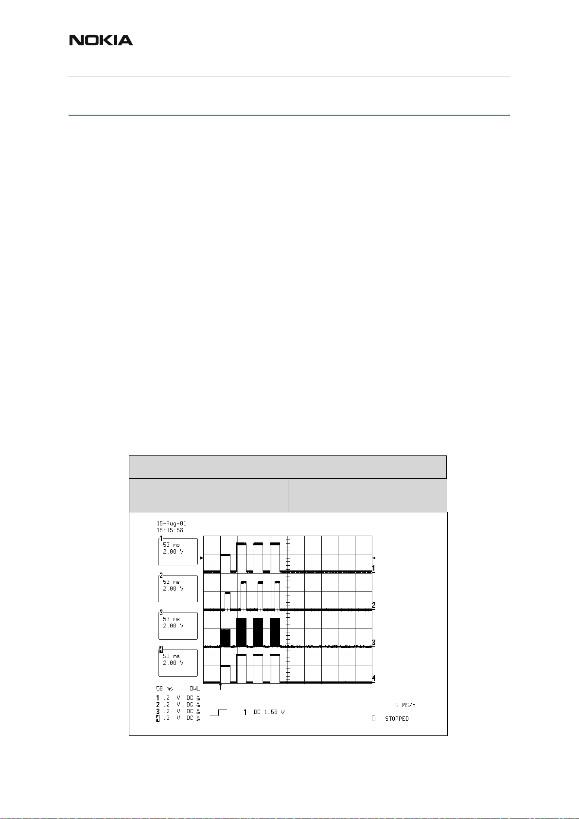
Analog Power control signals (TXC, VPC, VDET)
RH-53/54
The pictures in the following page show the typical shapes of the control signals low ba nd, right
side it for highest power – left side for lowest power . In all the pictures TXP is used a the trigger
point and is seen in the top of each picture. The difference between the high band and the low
band is that he high band signals looks the same with only small changes in level. The activating of high band Vdet starts 5us earlier than for low band.
58 COMPANY CONFIDENTIAL ISSUE 1 09/2004
Copyright © 2004 Nokia. All Rights Reserved.
Page 59

RH-53/54
Nokia Customer Care
Figure 46:Power control signals
High Power Low Power
TXC TXC
VPC VPC
VDET VDET
ISSUE 1 09/2004 COMPANY CONFIDENTIAL 59
Copyright © 2004 Nokia. All Rights Reserved.
Page 60

RH-53/54
Nokia Customer Care
I/Q signals
The following diagrams show different situations of TX IQ measurements. Depending on the
time the modulation may cause the signal to look different.
60 COMPANY CONFIDENTIAL ISSUE 1 09/2004
Copyright © 2004 Nokia. All Rights Reserved.
Page 61

RH-53/54
Nokia Customer Care
Alignment
■ Manual alignment with Phoenix
The alignment/calibration is the same in both GSM900/850 and GSM1800/1900 except for the
channels and frequencies. Only the the procedures for GSM900/GSM1800 are shown.
In Phoenix select connection Fbus scan product. If you power up the board before selecting
Fbus, it works without any error messages. Use Jig or other device for RF and bus connection.
Attenuation in the probe alone is 0dB for 900 and 0.1dB for 1800. Use CMD55,CMU200 or other suitable device. Default channels are 37 for GSM900 and 700 for GSM1800 (Ch 190 and
661 for GSM850/1900). The alignments and calibrations mu st be performed in the order shown
to give reliable results.
The way to save data to the phone and to load data from the phone is made different in the
various tunings. Always look what is shown in the windows regarding these issues and act accordingly . In some windows the saving is done without any warning or secon d approval as soon
as you stop or end.
To vary a selected parameter you can use + and – key or in some cases directly type the new
value. + and – steps the value for every press. Repeat function seems not to work. In I/Q you
can use the side arrows.
■ RX calibration
Select Tuning, RX Calibration
Select band GSM900
Press start
Figure 47:RX calibration
ISSUE 1 09/2004 COMPANY CONFIDENTIAL 61
Copyright © 2004 Nokia. All Rights Reserved.
Page 62

Nokia Customer Care
Follow the description in Phoenix, setting up the signal generator as described
Figure 48:Calibration tuning
RH-53/54
Press the OK button
Figure 49:Calibration tuning
Press the Save&Continue botton.
62 COMPANY CONFIDENTIAL ISSUE 1 09/2004
Copyright © 2004 Nokia. All Rights Reserved.
Page 63

RH-53/54
Nokia Customer Care
Follow the description in Phoenix, setting up the signal generator as described
Figure 50:Calibration tuning
Press the OK button
Figure 51:Calibration tuning
ISSUE 1 09/2004 COMPANY CONFIDENTIAL 63
Copyright © 2004 Nokia. All Rights Reserved.
Page 64

Nokia Customer Care
Press the Save&Continue botton
Note! You have to follow the shown procedure. It is not possible to tune the high band alone.
You need to make a tuning of the low band first to come to the high band. You can stop at any
time by switching off the menu. If the values are outside internal specs, you can not save them
and have to leave the tuning without saving.
■ RX Band Filter Response
Normally not needed in repair.
■ Tx Power tuning
Select Tuning, Tx Power Level Tuning
Figure 52:TX tuning
RH-53/54
Press start and follow the instructions in the pop-up window
Figure 53:TX tuning
64 COMPANY CONFIDENTIAL ISSUE 1 09/2004
Copyright © 2004 Nokia. All Rights Reserved.
Page 65

RH-53/54
Nokia Customer Care
Set the spectrum analyser or GSM tester for the required settings and press “OK” If a GSM
tester is used, set the TX data type to random so that the tester can trig on the signal.
Figure 54:TX tuning
Tune the highlighted values to the wanted power (Use average burst power)
Tune the base level to –25dBm
When done press Save&Continue and Phoenix will automatically shif t from lowband t o
highband. At the same time the intermidiate values are calculated, but that is firs t seen
next time you start a tuning.
Figure 55:TX tuning
ISSUE 1 09/2004 COMPANY CONFIDENTIAL 65
Copyright © 2004 Nokia. All Rights Reserved.
Page 66

RH-53/54
Nokia Customer Care
Set the spectrum analyser or GSM tester for the required settings and press “OK” . If a GSM
tester is used, set the TX data type to random so that the tester can trig on the signal.
Figure 56:TX tuning
Tune the highlighted values to the wanted power (Use average burst power).
Tune the base level to –25dBm.
When done press Save&Continue. The intermediate results are then calculated.
The procedure has to be followed. First low band tuning and then high band tuning. You do not
need to change anything.
■ I/Q tuning
Select Tuning, Tx IQ tuning, TX Data Type “random” for a GSM tester like CMU200 or 1/0 for
SPA measuring.
CMD55 shows the same as a spectrum analyzer when I/Q tuning is selected. CMU200 shows
the carrier and sideband supression directly as figures in the modulation mode.
66 COMPANY CONFIDENTIAL ISSUE 1 09/2004
Copyright © 2004 Nokia. All Rights Reserved.
Page 67

RH-53/54
Nokia Customer Care
Figure 57:i/Q tuning
Press Start
Figure 58:I/Q tuning
ISSUE 1 09/2004 COMPANY CONFIDENTIAL 67
Copyright © 2004 Nokia. All Rights Reserved.
Page 68

Nokia Customer Care
Set the spectrum analyser or GSM tester for the required settings and press “OK”
Figure 59:I/Q tuning
RH-53/54
Begin tuning with data from selected place.
Tune DC offset values to lowest carrier. Use Side arrows or +, - .
Tune Amplitude and phase to lowest sideband.
When satisfied with the result, press Next. (The sidebands should hardly be visible).Or for
CMU200 the supression should be better than -40dBc.
Figure 60:I/Q tuning
68 COMPANY CONFIDENTIAL ISSUE 1 09/2004
Copyright © 2004 Nokia. All Rights Reserved.
Page 69

RH-53/54
Nokia Customer Care
Set the spectrum analyser or GSM tester for the required settings and press “OK”
Figure 61:I/Q tuning
Press Start to begin tuning with data from selected place.
Tune DC offset values to lowest carrier. Use Side arrows or +, - .
Tune Amplitude and phase to lowest sideband.
When satisfied with the result, press Finish. (The sidebands should hardly be visible).
■ RF control
The purpoase is to check the receiver or transmitter without going in call. It works very much
like a call, but you have control via the PC and not via the tester . If you want to tune or calibrat e
at other channels or levels than the default for that function, you can activate RF control at the
same time and change the wanted parameters.
Figure 62:RF controls
ISSUE 1 09/2004 COMPANY CONFIDENTIAL 69
Copyright © 2004 Nokia. All Rights Reserved.
Page 70

RH-53/54
Nokia Customer Care
Autotune (RH-53 with CMU200)
■ File adjustments
Edit the file RH_53_tunings.ini and save it in the product folder under Phoenix with the right
name. It defines the target values for the tu nings which need targets or can be a general one
that only needs small updates for the values that might change (e.g. the base target).
Edit the file autotune_RH-53.ini and save it in the product folder under Phoenix with the right
name.
Change the Baselevel init values so that the expected base coefficient is among them. It is not
absolutely needed but it speeds up the tuning. Larger steps can be used but with lower accuracy.
Eventually, change also the Coeff init values if the tuning deviates too much from the target.
The lowest coefficient must be very close to 0. Check how the power tuning goes an d try with
some changes.
In case of edge capability, copy from RH-12 and make some changes. RH-12 is for Gemini engine, RH-53 is for Mjoelner engine.
For autotuning, please see also TB “Autotuning function in Phoenix”.
■ Phoenix setup
In Phoenix tools-options-gpib card select the type of card used.
Press start to check if the equipment can be found.
Figure 63:Phoenix-GPIB card
70 COMPANY CONFIDENTIAL ISSUE 1 09/2004
Copyright © 2004 Nokia. All Rights Reserved.
Page 71

RH-53/54
Nokia Customer Care
With a PKD-1NS dongle the loss in cables and jigs has to be set, and the jig type must be defined to the product. When that is done the PKD-1 donkle can be used, and the losses can not
be changed with that dongle.
Figure 64:Set loss
Select or add a jig and define the losses
Figure 65:Set loss 2
ISSUE 1 09/2004 COMPANY CONFIDENTIAL 71
Copyright © 2004 Nokia. All Rights Reserved.
Page 72

RH-53/54
Nokia Customer Care
Make sure the product has the right type of jig. (At the moment new products like RH-54 can
not be added)
Figure 66:Set loss 3
Note! CMU200:
Remember that CMU200 is left as it was set in the autotune. Attenuation settings are at 0.
72 COMPANY CONFIDENTIAL ISSUE 1 09/2004
Copyright © 2004 Nokia. All Rights Reserved.
 Loading...