


DATA SHEET
PHOTOCOUPLER
PS9713
1 Mbps, OPEN COLLECTOR OUTPUT, FOR GATE DRIVE INTERFACE
INTELLIGENT POWER MODULE
5-PIN SOP PHOTOCOUPLER
DESCRIPTION
The PS9713 is an optically coupled isolator containing a GaAlAs LED on the input side and a photo diode and a
signal processing circuit on the output side on one chip.
FEATURES
• High instantaneous common mode rejection voltage (CMH, CML = ±15 kV/µs MIN.)
• Small package (5-pin SOP)
• High-speed response (t
• Maximum propagation delays (t
• Pulse width distortion ( | t
• Ordering number of taping product: PS9713-F3, F4: 3 500 pcs/reel
• UL approved: File No. E72422 (S)
• VDE0884 approved (Option)
PHL
= 500 ns MAX., t
PLH
− t
PHL
PLH
− t
| = 270 ns TYP.)
PLH
= 750 ns MAX.)
PHL
= 270 ns TYP.)
−NEPOCTM Series−
APPLICATIONS
•IPM Driver
• General purpose inverter
The information in this document is subject to change without notice. Before using this document, please
confirm that this is the latest version.
Not all devices/types available in every country. Please check with local NEC representative for
availability and additional information.
Document No. P13982EJ2V0DS00 (2nd edition)
Date Published May 2000 NS CP(K)
Printed in Japan
©
1998, 2000

PACKAGE DIMENSIONS (in millimeters)
4.0±0.5
2.1±0.2
1.27
+0.10
–0.05
0.15
TOP VIEW
64
5
13
7.0±0.3
4.4
0.5±0.3
1. Anode
3. Cathode
4. GND
O
5. V
6. V
CC
PS9713
0.4
0.1±0.1
FUNCTIONAL DIAGRAM
1
3
LED
+0.10
–0.05
Output
0.25 M
6
5
4
Shield
ON L
OFF
2
H
Data Sheet P13982EJ2V0DS00
ORDERING INFORMATION
PS9713
Part Number Package Packing Style
Safety Standards
Approval
Application Part
PS9713 5-pin SOP Magazine case 100 pcs UL approved PS9713
PS9713-F3 Embossed Tape 3 500 pcs/reel
PS9713-F4
PS9713-V Magazine case 100 pcs VDE0884 approved
PS9713-V-F3 Embossed Tape 3 500 pcs/reel
PS9713-V-F4
For the application of the Safety Standard, following part number should be used.
*1
ABSOLUTE MAXIMUM RATINGS (TA = 25 °°°°C, unless otherwise specified)
Parameter Symbol Ratings Unit
Diode Forward Current I
Reverse Voltage V
Detector
Supply Voltage V
Output Voltage V
Output Current I
Power Dissipation P
Isolation Voltage
*1
Operating Ambient Temperature T
Storage Temperature T
F
R
CC
O
O
C
25 mA
3.0 V
−
0.5 to +35 V
−
0.5 to +35 V
15 mA
100 mW
BV 2 500 Vr.m.s .
A
stg
−
40 to +100
−
55 to +125
°
C
°
C
Number
*1
AC voltage for 1 minute at T
*1
A
= 25 °C, RH = 60 % between input and output.
RECOMMENDED OPERATING CONDITIONS
Parameter Symbol MIN. TYP. MAX. Unit
High Level Input Current I
Output Voltage V
Supply Voltage V
LED Off Voltage V
FH
O
CC
F
10 20 mA
030V
4.5 30 V
00.8V
Data Sheet P13982EJ2V0DS00
3

PS9713
ELECTRICAL CHARACTERISTICS (TA = −−−−40 to +100 °°°°C, VCC = 15 V, unless otherwise specified)
*1
Parameter Symbol Conditions MIN.
TYP.
MAX. Unit
Diode Forward Voltage V
Reverse Current I
Terminal Capacitance CtV = 0 V, f = 1 MHz, TA = 25 °C30pF
Detector Low Level Output Voltage V
High Level Output Current I
High Level Supply Current I
Low Level Supply Current I
Coupled
Threshold Input Current
(H → L)
Current Transfer Ratio (IC/IF)CTRIF = 10 mA, VO = 0.6 V 44 110 %
Isolation Resistance R
Isolation Capacitance C
Propagation Delay Time
*2
(H → L)
Propagation Delay Time
*2
(L → H)
Maximum Propagation
PLH
t
Delays
Pulse Width Distorti on
*2
(PWD)
Instantaneous Common
Mode Rejection Voltage
(Output: High)
*3
Instantaneous Common
Mode Rejection Voltage
(Output: Low)
*3
PHL
|t
CM
CM
FIF
= 10 mA 1.3 1.65 2.1 V
R
VR = 3 V 200
OLIF
= 10 mA, VCC = 5 V, IO = 2.4 mA 0.13 0.6 V
OH
VCC = 30 V, VF = 0.8 V 1.0 50
CCH
VCC = 30 V, VF = 0.8 V, VO = open 0.6 1.3 mA
CCL
VCC = 30 V, IF = 10 mA, VO = open 0.6 1.3 mA
FHL
I
VO = 0.8 V, IO = 0.75 mA 1.5 5.0 mA
I-O
V
I-O
I-O
PHL
t
PLH
t
−
t
−
t
= 1 kVDC, RH = 40 to 60 %,
A
T
= 25 °C
V = 0 V, f = 1 MHz, TA = 25 °C0.6pF
IF = 10mA, RL = 20 kΩ, CL = 100 pF,
THHL
V
= 1.5 V, V
PHL
PLH
| 270 650
TA = 25 °C, IF = 0 mA, VO > 3.0 V,
H
CM
V
= 1.5 kV, RL = 20 kΩ,
L
C
= 100 pF
TA = 25 °C, IF = 10 mA, VO < 1.0 V,
L
CM
V
= 1.5 kV, RL = 20 kΩ,
L
C
= 100 pF
THLH
= 2.0 V
11
10
250 500 ns
520 750
−
200 270 650
15 kV/
15 kV/
µ
A
µ
A
Ω
µ
s
µ
s
4
Data Sheet P13982EJ2V0DS00

A
Typical values at T
*1
Test circuit for propagation delay time
*2
= 25 °C.
PS9713
Pulse input (IF = 10 mA)
(PW = 10 s,
µ
0.1 F
Duty cycle = 1/10)
Input
(Monitor)
47 Ω
CL is approximately which includes probe and stray wiring capacitance.
Test circuit for common mode transient immunity
*3
GL SW I
F
0.1 F
µ
BA
V
CM
CL is approximately which includes probe and stray wiring capacitance.
µ
L
= 20 kΩ
R
C
L
= 100 pF
RL = 20 kΩ
CL = 100 pF
CC
= 15 V
V
O
(Monitor)
V
V
CC
= 15 V
O
(Monitor)
V
THHL
= 1.5 V
V
V
CM
V
O
(Switch A: IF = 0 mA)
V
O
(Switch B: IF = 10 mA)
Input
Output
t
PHL
90 %
10 %
IF (ON)
50 % I
F
(ON)
15 V
V
THLH
= 2.0 V
V
t
PLH
OL
1.5 kV
0 V
t
r
t
f
15 V
3.0 V
1.0 V
V
OL
USAGE CAUTION
By-pass capacitor of more than 0.1 µF is used between VCC and GND near device. Also, ensure that the distance
between the leads of the photocoupler and capacitor is no more than 10 mm.
Data Sheet P13982EJ2V0DS00
5

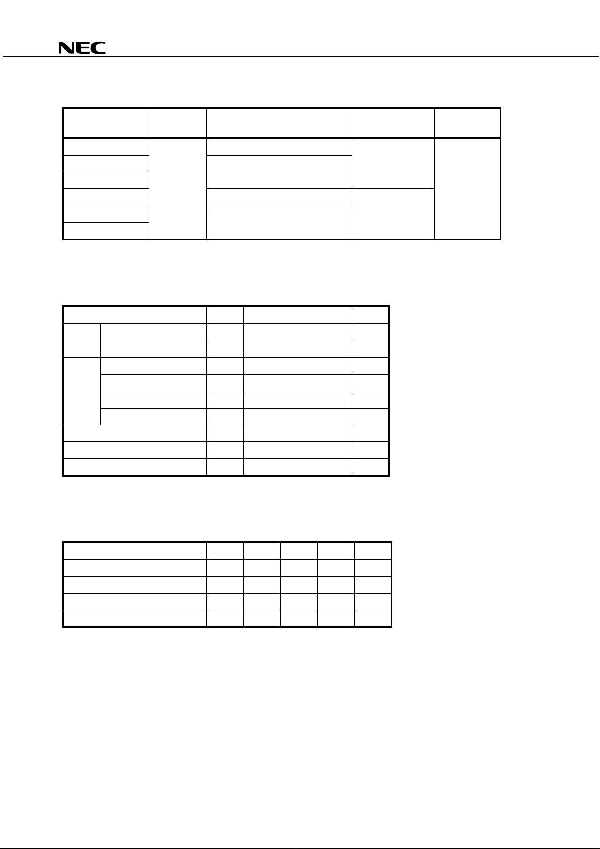
TYPICAL CHARACTERISTICS (TA = 25 °°°°C, unless otherwise specified)
PS9713
MAXIMUM FORWARD CURRENT
vs. AMBIENT TEMPERATURE
40
(mA)
F
30
20
10
Maximum Forward Current I
20 40 60 80 1000
Ambient T emperature T
FORWARD CURRENT vs.
FORWARD VOLTAGE
100
10
(mA)
F
1
0.1
Forward Current I
0.01
1.0
1.2 1.4 1.6 1.8 2.0 2.2 2.4
Forward V oltage VF (V)
A
(˚C)
TA = +85 ˚C
+50 ˚C
+25 ˚C
0 ˚C
–25 ˚C
DETECTOR POWER DISSIPATION
vs. AMBIENT TEMPERATURE
150
(mW)
C
100
50
Detector Power Dissipation P
20 40 60 80 1000
Ambient T emperature TA (˚C)
SUPPLY CURRENT vs.
AMBIENT TEMPERATURE
1 200
µ
µ
( A),
1 000
( A)
CCH
CCL
800
600
400
200
High Level Supply Current I
Low Level Supply Current I
0
–50 –25 0 25 50 75 100
Ambient T emperature TA (˚C)
V
V
I
I
CCH
CCL
CC
= 30 V,
O
= Open,
: VF = 0.8 V,
: IF = 10 mA
CCL
I
I
CCH
THRESHOLD INPUT CURRENT vs.
AMBIENT TEMPERATURE
5
(mA)
4
FHL
3
2
1
Threshold Input Current I
0
–50 –25 0 25 50 75 100
Ambient T emperature TA (˚C)
6
VCC = 15 V,
O
= 0.8 V,
V
O
= 0.75 mA
I
Data Sheet P13982EJ2V0DS00
LOW LEVEL OUTPUT VOLTAGE vs.
AMBIENT TEMPERATURE
0.6
(V)
0.5
OL
0.4
0.3
0.2
0.1
Low Level Output Voltage V
0
–50 –25
Ambient T emperature TA (˚C)
250 50 75 100
VCC = 15 V,
F
= 10 mA,
I
O
= 2.4 mA
I

OUTPUT CURRENT vs. FORWARD CURRENT
14
12
10
(mA)
O
TA = +25 ˚C
8
6
4
+100 ˚C
–40 ˚C
Output Current I
2
0
0 5 10 15 20
Forward Current IF (mA)
V
O
= 0.6 V
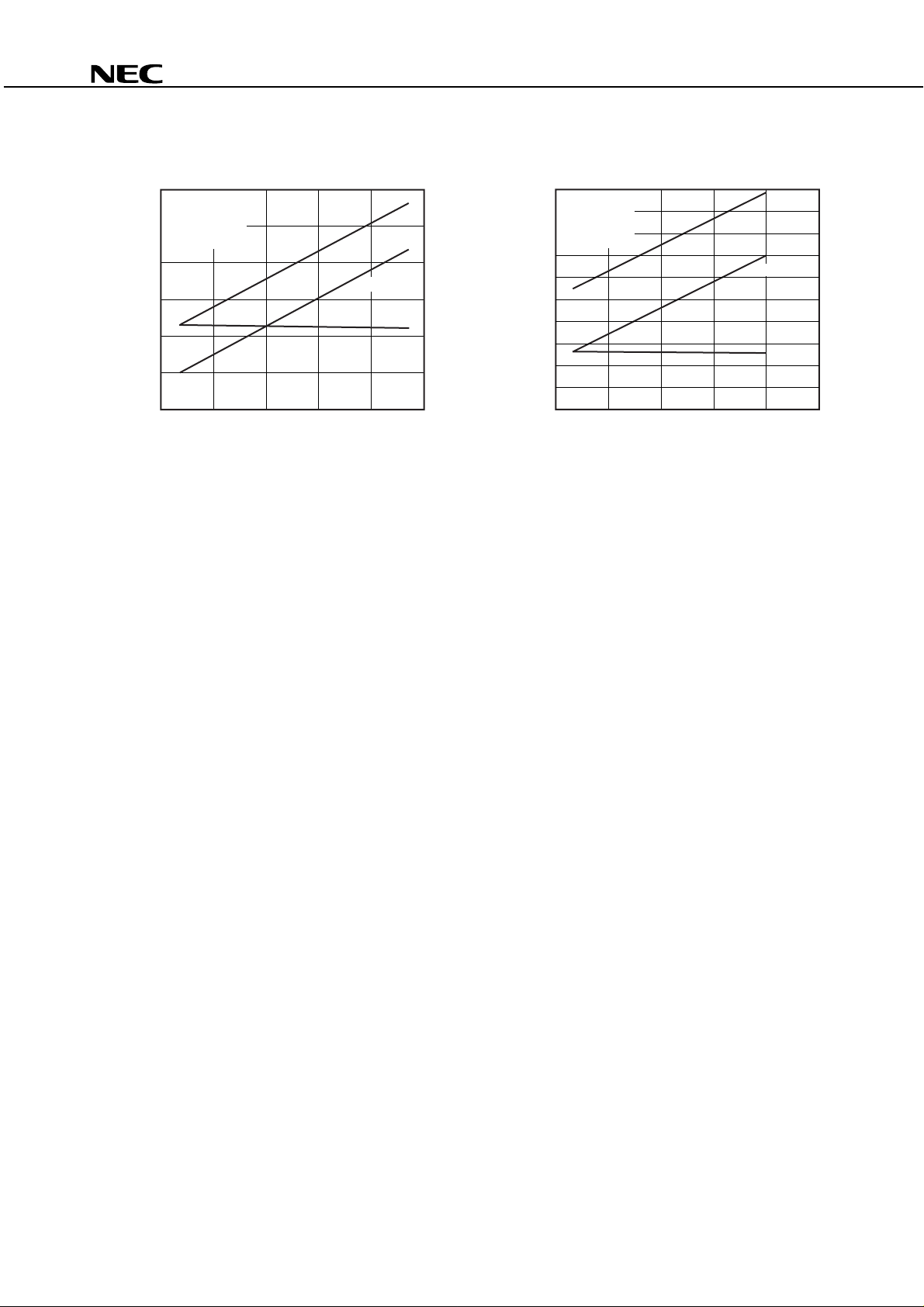
PROPAGATION DELAY TIME,
MAXIMUM PROPAGATION DELAYS
vs. FORWARD CURRENT
700
(ns)
V
CC
PHL
– t
(ns),
PLH
PLH
, t
PHL
600
500
400
300
200
= 15 V,
L
= 100 pF,
C
L
= 20 kΩ
R
t
PLH
t
PHL
t
PLH
– t
PHL
100
0
0 5 10 15 20
Maximum Propagation Delays t
Propagation Delay Time t
F
Forward Current I
(mA)
PROPAGATION DELAY TIME,
PULSE WIDTH DISTORTION
vs. AMBIENT TEMPERATURE
700
(ns),
(ns)
600
PLH
PLH
, t
PHL
Propagation Delay Time t
t
PLH
– t
500
PHL
400
t
PHL
300
200
PWD
100
Pulse Width Distortion t
0
–40 –20 0 20 40 60 80 100
IF = 10 mA,
CC
= 15 V,
V
L
= 100 pF,
C
L
= 20 kΩ
R
Ambient T emperature TA (˚C)
OUTPUT CURRENT vs.
AMBIENT TEMPERATURE
1.10
I
F
= 10 mA,
O
= 0.6 V
V
1.05
1.00
0.95
0.90
0.85
0.80
Output Current (Relative Value)
0.75
0.70
–40 –20 0 20 40 60 80 100
Ambient T emperature T
PROPAGATION DELAY TIME,
MAXIMUM PROPAGATION DELAYS
vs. SUPPLY VOLTAGE
1 800
(ns)
PHL
1 600
– t
1 400
(ns),
PLH
PLH
1 200
, t
PHL
1 000
800
600
t
PLH
t
PHL
t
PLH
– t
PHL
–200
Maximum Propagation Delays t
Propagation Delay Time t
400
200
0
010203040
Supply Voltage VCC (V)
PROPAGATION DELAY TIME vs.
LOAD CAPACITANCE
1 600
F
= 10 mA,
(ns)
PLH
, t
PHL
Propagation Delay Time t
I
1 400
L
= 20 kΩ
R
CC
= 15 V,
V
1 200
1 000
800
600
400
200
0
0 100 200 300 400
Load Capacitance CL (pF)
A
(˚C)
F
= 10 mA,
I
L
= 100 pF,
C
L
= 20 kΩ
R
PS9713
t
PLH
t
PHL
500
Data Sheet P13982EJ2V0DS00
7
PS9713
1 000
800
PLH – tPHL (ns)
600
400
200
–200
Maximum Propagation Delays t
Propagation Delay Time tPHL, tPLH (ns),
Remark
PROPAGATION DELAY TIME,
MAXIMUM PROPAGATION DELAYS
vs. LOAD RESISTANCE
IF = 10 mA,
VCC = 15 V,
CL = 100 pF
0
010203040
Load Resistance RL (kΩ)
The graphs indicate nominal characteristics.
tPLH
tPLH – tPHL
t
PHL
50
PROPAGATION DELAY TIME,
MAXIMUM PROPAGATION DELAYS
vs. LOAD RESISTANCE
500
I
F = 10 mA,
450
VCC = 5 V,
CL = 15 pF
400
PLH – tPHL (ns)
350
300
250
200
150
100
50
0
0 5 10 15 20
Maximum Propagation Delays t
Propagation Delay Time tPHL, tPLH (ns),
Load Resistance RL (kΩ)
tPLH
tPLH – tPHL
tPHL
25
8
Data Sheet P13982EJ2V0DS00

TAPING SPECIFICATIONS (in millimeters)
Outline and Dimensions (Tape)
2.0±0.1
4.0±0.1
1.55±0.1
1.75±0.1
PS9713
2.4±0.1
1.55±0.1
8.0±0.1
Tape Direction
PS9713-F3
Outline and Dimensions (Reel)
4.6±0.1
1
2
0
5.5±0.1
˚
12.0±0.2
PS9713-F4
7.4±0.1
0.3
1.5
2.0±0.5
1.5±0.5
6
0
˚
Packing: 3 500 pcs/reel
Data Sheet P13982EJ2V0DS00
21.0±0.8
φ
6.0±1
330
φ
80±5.0
13.0±0.5
φ
φ
12.4
+2.0
–0.0
9
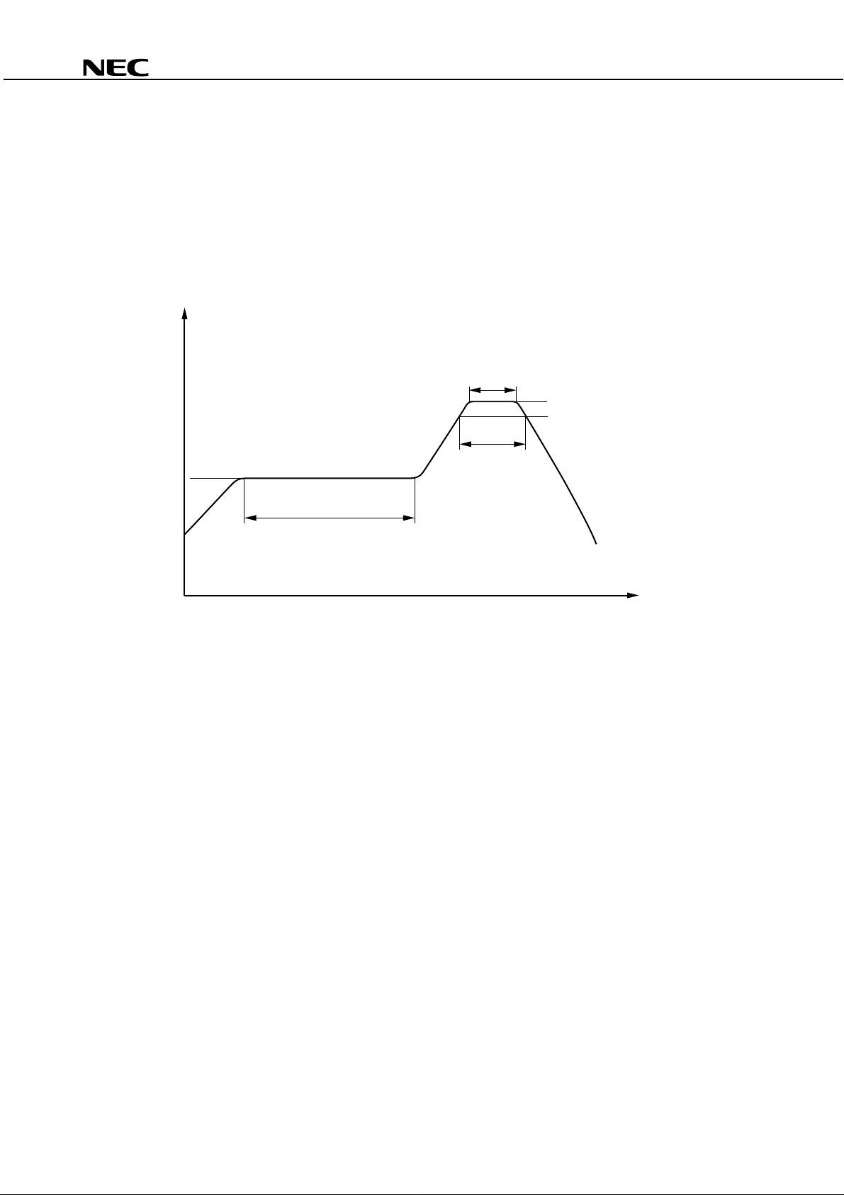
RECOMMENDED SOLDERING CONDITIONS
(1) Infrared reflow soldering
• Peak reflow temperature 235 °C or below (package surface temperature)
• Time of temperature higher than 210 °C 30 seconds or less
• Number of reflows Three
• Flux Rosin flux containing small amount of chlorine (The flux with a
maximum chlorine content of 0.2 Wt % is recommended.)
Recommended Temperature Profile of Infrared Reflow
(heating)
to 10 s
235 ˚C (peak temperature)
210 ˚C
to 30 s
100 to 160 ˚C
PS9713
60 to 120 s
(preheating)
Package Surface Temperature T (˚C)
Time (s)
(2) Dip soldering
• Temperature 260 °C or below (molten solder temperature)
• Time 10 seconds or less
• Number of times One (Allowed to be dipped in solder including plastic mold portion.)
• Flux Rosin flux containing small amount of chlorine (The flux with a maximum chlorine content of
0.2 Wt % is recommended.)
(3) Cautions
•Fluxes
Avoid removing the residual flux with freon-based and chlorine-based cleaning solvent.
10
Data Sheet P13982EJ2V0DS00

CAUTION
Within this device there exists GaAs (Gallium Arsenide) material which is a
harmful substance if ingested. Please do not under any circumstances break the
hermetic seal.
PS9713
Data Sheet P13982EJ2V0DS00
11

PS9713
NEPOC is a trademark of NEC Corporation.
•
The information in this document is current as of May, 2000. The information is subject to change
without notice. For actual design-in, refer to the latest publications of NEC's data sheets or data
books, etc., for the most up-to-date specifications of NEC semiconductor products. Not all products
and/or types are available in every country. Please check with an NEC sales representative for
availability and additional information.
•
No part of this document may be copied or reproduced in any form or by any means without prior
written consent of NEC. NEC assumes no responsibility for any errors that may appear in this document.
•
NEC does not assume any liability for infringement of patents, copyrights or other intellectual property rights of
third parties by or arising from the use of NEC semiconductor products listed in this document or any other
liability arising from the use of such products. No license, express, implied or otherwise, is granted under any
patents, copyrights or other intellectual property rights of NEC or others.
•
Descriptions of circuits, software and other related information in this document are provided for illustrative
purposes in semiconductor product operation and application examples. The incorporation of these
circuits, software and information in the design of customer's equipment shall be done under the full
responsibility of customer. NEC assumes no responsibility for any losses incurred by customers or third
parties arising from the use of these circuits, software and information.
•
While NEC endeavours to enhance the quality, reliability and safety of NEC semiconductor products, customers
agree and acknowledge that the possibility of defects thereof cannot be eliminated entirely. To minimize
risks of damage to property or injury (including death) to persons arising from defects in NEC
semiconductor products, customers must incorporate sufficient safety measures in their design, such as
redundancy, fire-containment, and anti-failure features.
•
NEC semiconductor products are classified into the following three quality grades:
"Standard", "Special" and "Specific". The "Specific" quality grade applies only to semiconductor products
developed based on a customer-designated "quality assurance program" for a specific application. The
recommended applications of a semiconductor product depend on its quality grade, as indicated below.
Customers must check the quality grade of each semiconductor product before using it in a particular
application.
"Standard": Computers, office equipment, communications equipment, test and measurement equipment, audio
and visual equipment, home electronic appliances, machine tools, personal electronic equipment
and industrial robots
"Special": Transportation equipment (automobiles, trains, ships, etc.), traffic control systems, anti-disaster
systems, anti-crime systems, safety equipment and medical equipment (not specifically designed
for life support)
"Specific": Aircraft, aerospace equipment, submersible repeaters, nuclear reactor control systems, life
support systems and medical equipment for life support, etc.
The quality grade of NEC semiconductor products is "Standard" unless otherwise expressly specified in NEC's
data sheets or data books, etc. If customers wish to use NEC semiconductor products in applications not
intended by NEC, they must contact an NEC sales representative in advance to determine NEC's willingness
to support a given application.
(Note)
(1) "NEC" as used in this statement means NEC Corporation and also includes its majority-owned subsidiaries.
(2) "NEC semiconductor products" means any semiconductor product developed or manufactured by or for
NEC (as defined above).
M8E 00. 4
 Loading...