

DATA SHEET
PHOTOCOUPLER
PS9711
HIGH NOISE REDUCTION/HIGH-SPEED 10 Mbps, TOTEM-POLE OUTPUT TYPE
5-PIN SOP TOM PHOTOCOUPLER
DESCRIPTION
The PS9711 is an optically coupled high-speed, totem-pole output isolator containing a GaAlAs LED on light
emitting diode (input) and a photodiode and a signal processing circuit on light receiving side (output side) on one
chip.
FEATURES
• High common mode transient immunity (CMH, CML = ±10 kV/µs TYP.)
• Small package (5-pin SOP)
• High-speed response (t
• Pulse width distortion (t
• Totem-pole output (No pull-up resistor required)
• Ordering number of taping product: PS9711-E3, E4: 900 pcs/reel,
PHL
= 30 ns, t
PHL
– t
PLH
= 35 ns TYP.)
PLH
= 7 ns TYP.)
PS9711-F3, F4 (Recommended): 3 500 pcs/reel
−NEPOCTM Series−
APPLICATIONS
• Computer and peripheral manufactures
• Measurement equipment
•PDP
The information in this document is subject to change without notice. Before using this document, please
confirm that this is the latest version.
Not all devices/types available in every country. Please check with local NEC representative for
availability and additional information.
Document No. P13103EJ3V0DS00 (3rd edition)
Date Published February 2000 NS CP(K)
Printed in Japan
The mark
••••
shows major revised points.
©
1997, 2000
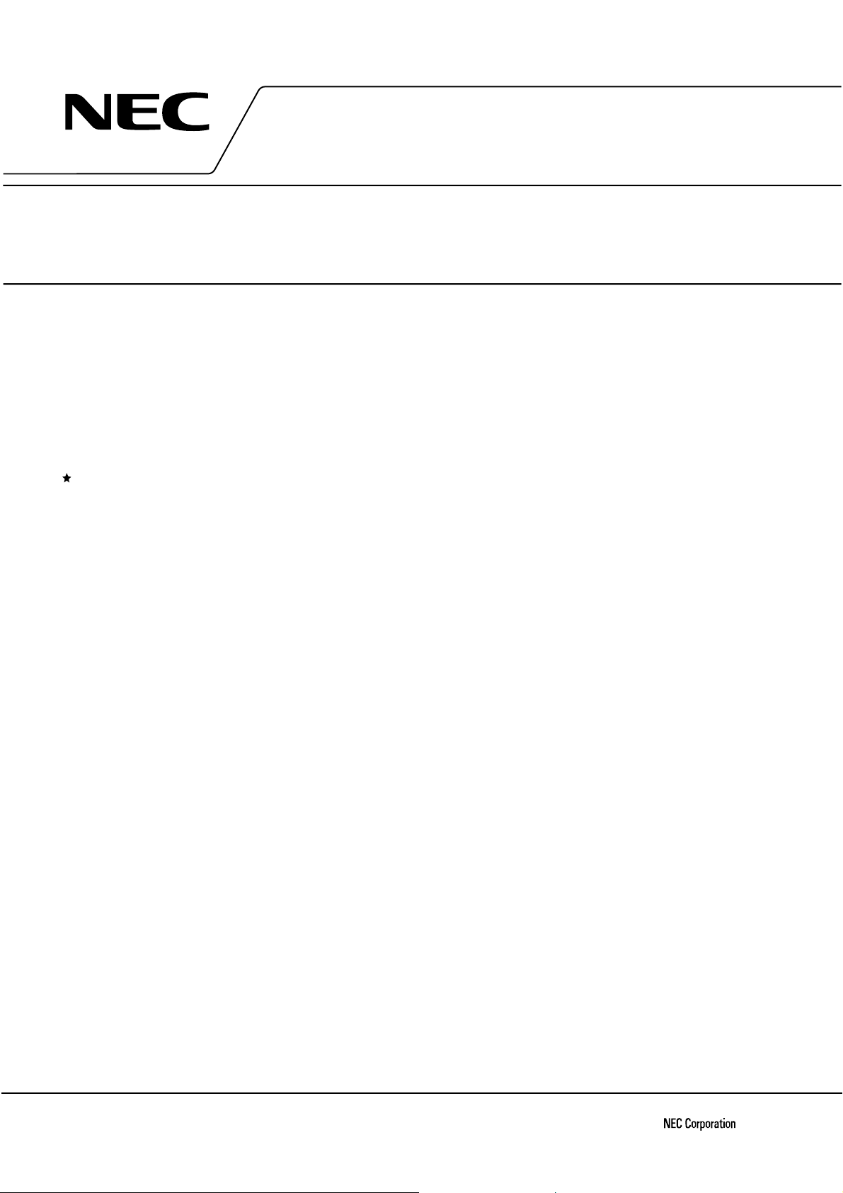
PACKAGE DIMENSIONS (in millimeters)
4.0±0.5
2.1±0.2
1.27
+0.10
–0.05
0.15
TOP VIEW
53
4
12
7.0±0.3
4.4
0.5±0.3
1. Anode
2. Cathode
3. GND
4. V
O
5. V
CC
PS9711
+0.10
0.4
0.1±0.1
–0.05
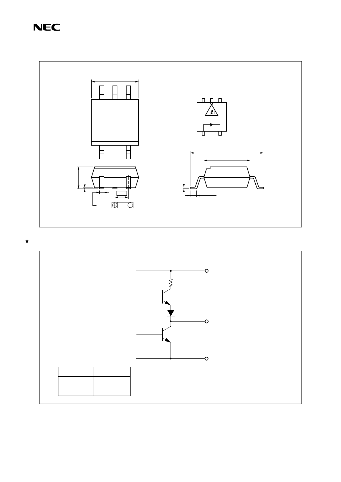
INTERNAL OUT PUT CIRCUIT
0.25 M
V
CC
(5)
Vo (4)
GND (3)
LED
Output
ON L
OFF
2
H
Data Sheet P13103EJ3V0DS00
ORDERING INFORMATION
PS9711
Part Number Package Packing Style
Application Part Number
PS9711 5-pin SOP Magazine case 100 pcs PS9711
PS9711-E3 Embossed Tape 900 pcs/reel
PS9711-E4
PS9711-F3 Emboss ed Tape 3 500 pcs/reel
PS9711-F4
For the application of the Safety Standard, following part number should be used.
*1
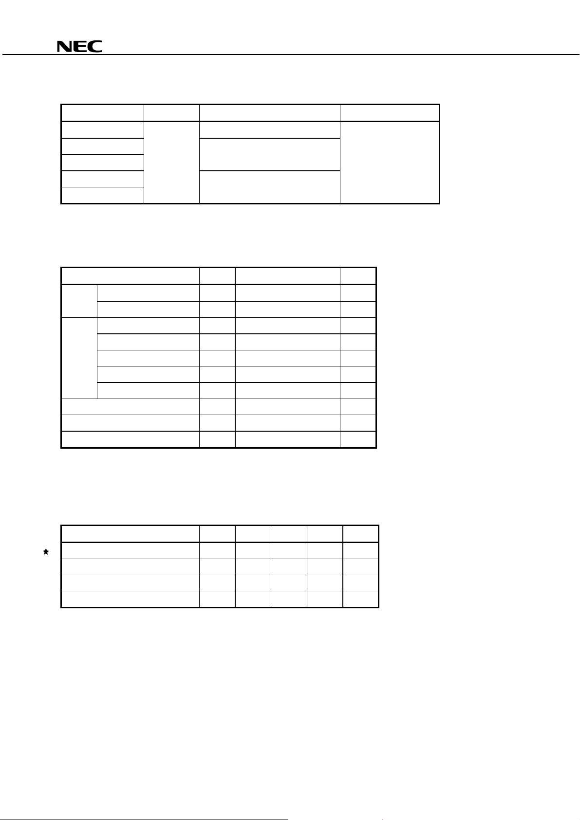
ABSOLUTE MAXIMUM RATINGS (TA = 25 °°°°C, unless otherwise specified)
Parameter Symbol Ratings Unit
Diode Forward Current I
Reverse Voltage V
Detector
Supply Voltage V
Output Voltage V
High Level Output Current
Low Level Output Current
Power Dissipation
Isolation Voltage
*2
*1
Operating Ambient Temperature T
Storage Temperature T
F
R
CC
O
*1
OH
I
*1
OL
I
C
P
30 mA
3.0 V
7V
7V
−
5mA
13 mA
130 mW
BV 2 500 Vr.m.s.
A
stg
−
40 to +85
−
55 to +125
°
C
°
C
*1
A
T
= −40 to +85 °C
*1
AC voltage for 1 minute at TA = 25 °C, RH = 60 % between input and output.
*2
RECOMMENDED OPERATING CONDITIONS
Parameter Symbol MIN. TYP. MAX. Unit
High Level Input Current I
Low Level Input Current I
Supply Voltage V
TTL (loads) N 3
FH
FL
CC
7.5 12.5 mA
0 250
4.5 5.0 5.5 V
µ
A
Data Sheet P13103EJ3V0DS00
3
ELECTRICAL CHARACTERISTICS (TA = −−−−40 to +85 °C, unless otherwise specified)
Parameter Symbol Conditions MIN.
TYP.
*1
MAX. Unit
PS9711
Diode Forward Voltage V
Reverse Current I
Terminal Capacitance C
Detector High Level Output Current I
High Level Output Voltage V
Low Level Output Voltage V
High Level Supply Current I
Low Level Supply Current I
High Level Output Short
I
Circuit Current
Low Level Output Short
Circuit Current
Coupled Threshold Input Current I
(H → L) 6
Threshold Input Current I
(L → H) 0.35
Isolation Resistance R
Isolation Capacitance C
Propagation Delay Time t
*2
(H → L)
Propagation Delay Time t
*2
(L → H)
PHL-tPLH
Pulse Width Distorti on
*2
(PWD)
Common Mode
Transient Immunity at Hi gh
Level Output
*3
Common Mode
Transient Immunity at Low
Level Output
*3
t
CM
CM
F
IF = 10 mA, TA = 25 °C 1.4 1.65 1.9 V
R
VR = 3 V, TA = 25 °C10
t
V = 0 V, f = 1 MHz, TA = 25 °C30pF
OH
VCC = VO = 5.5 V, IF = 250 µA 1 200
OH
VCC = 4.5 V, IF = 250 µA, IOH = −2 mA 2.4 3.0 V
OL
VCC = 4.5 V, IF = 7 mA, IO = 8 mA 0.38 0.6 V
CCH
VCC = 5.5 V, IF = 0 mA 11 17 mA
CCL
VCC = 5.5 V, IF = 10 mA 12 18 mA
VCC = 5.5 V, VO = GND, IF = 0 mA,
OSH
–26 mA
µ
A
µ
A
10 ms or less
VCC = VO = 5.5 V, IF = 8 mA,
OSL
I
34 mA
10 ms or less
FHL
VCC = 5 V TA = 25 °C2.05mA
FLH
VCC = 5 V TA = 25 °C0.5 mA
I-O
V
I-O
I-O
PHL
= 1 kVDC, RH = 40 to 60 %,
A
T
= 25 °C
V = 0 V, f = 1 MHz, TA = 25 °C0.4pF
TA = 25 °C 153065ns
10
11
Ω
VCC = 5 V, IF = 7.5 mA 10 85
PLH
TA = 25 °C 153565ns
VCC = 5 V, IF = 7.5 mA 10 85
CC
V
= 5 V, IF = 7.5 mA 7 35 ns
VCC = 5 V, TA = 25 °C, IF = 0 mA,
H
O (MIN.)
V
= 2 V, VCM = 100 V
VCC = 5 V, TA = 25 °C, IF = 7.5 mA,
L
O (MAX.)
V
= 0.8 V, VCM = 100 V
110 kV/
110 kV/
µ
s
µ
s
4
Data Sheet P13103EJ3V0DS00

PS9711
Typical values at T
*1
Test circuit for propagation delay time
*2
Pulse input (I
F
)
A
= 25 °C
V
CC
= 5 V
(PW = 500 ns,
V
GND
CC
µ
0.1 F
Duty cycle = 1/2)
Input
(monitor)
L
= 15 pF
C
47 Ω
CL is approximately which includes probe and stray wiring capacitance.
Test circuit for common mode transient immunity
*3
F
GL SW I
V
CC
µ
0.1 F
GND
CL is approximately which includes probe and stray wiring capacitance.
O
V
CL =
30 pF
CL = 15 pF
(monitor)
2.5 kΩ
V
CC
= 5 V
VO (Monitor)
V
CC
= 5 V
Input
1.3 kΩ
50 % I
IF (ON)
F
(ON)
OH
V
Output
1.5 V
V
OL
100 V
0 V
OH
V
2 V
V
CM
VO
(I
t
PHL
90 %
10 %
F
= 0 mA)
t
PLH
t
r
t
f
0.8 V
O
V
OL
V
(IF = 7.5 mA)
USAGE CAUTIONS
1. This product is weak for static electricity by designed with high-speed integrated circuit so protect against static
electricity when handling.
2. By-pass capacitor of more than 0.1 µF is used between VCC and GND near device.
Data Sheet P13103EJ3V0DS00
5

TYPICAL CHARACTERISTICS (TA = 25 °°°°C, unless otherwise specified)
PS9711
MAXIMUM FORWARD CURRENT
vs. AMBIENT TEMPERATURE
40
30
20
10
Maximum Forward Current IF (mA)
20 40 60 80 1000 20 40 60 80
Ambient T emperature TA (˚C)
FORWARD CURRENT vs.
FORWARD VOLTAGE
100
10
1
0.1
Forward Current IF (mA)
0.01
1.0
1.4 1.6 1.8 2.0 2.2 2.4
1.2
Forward V oltage V
TA = +85 ˚C
+50 ˚C
+25 ˚C
0 ˚C
–25 ˚C
F (V)
DETECTOR POWER DISSIPATION
vs. AMBIENT TEMPERATURE
150
100
50
Detector Power Dissipation PC (mW)
Ambient T emperature TA (˚C)
SUPPLY CURRENT vs.
AMBIENT TEMPERATURE
20
18
16
CCL (mA)
14
12
10
8
6
4
2
High Level Supply Current ICCH (mA),
Low Level Supply Current I
0
–50 –25 0 25 50 75 100
Ambient T emperature TA (˚C)
V
CC = 5.5 V,
CCH : IF = 0 mA,
I
CCL : IF = 10 mA
I
CCL
I
ICCH
8585
1000
HIGH LEVEL OUTPUT VOLTAGE vs.
HIGH LEVEL OUTPUT CURRENT
5
4
3
2
1
High Level Output Voltage VOH (V)
0
TA = +85 ˚C
+25 ˚C
–40 ˚C
–1 –2 –3 –5–4 –6
High Level Output Current IOH (mA)
6
VCC = 4.5 V,
µ
I
F = 250 A
Data Sheet P13103EJ3V0DS00
HIGH LEVEL OUTPUT VOLTAGE vs.
AMBIENT TEMPERATURE
5
4
3
2
1
High Level Output Voltage VOH (V)
0
–50 –25
Ambient T emperature TA (˚C)
VCC = 4.5 V, IF = 250 A,
I
OH = –2 mA
250 50 75 100
µ

PS9711
(V)
OL
Low Level Output Voltage V
(ns),
(ns)
PLH
PLH
, t
– t
PHL
PHL
Pulse Width Distortion t
Propagation Delay Time t
LOW LEVEL OUTPUT VOLTAGE vs.
LOW LEVEL OUTPUT CURRENT
3
V
CC
= 4.5 V,
F
= 7 mA
I
2
TA = +85 ˚C
1
0
Low Level Output Current I
+25 ˚C
–40 ˚C
10515
OL
PROPAGATION DELAY TIME,
PULSE WIDTH DISTORTION
vs. FORWARD CURRENT
70
60
50
40
30
20
10
–10
–20
–30
0
0
5 10152025
Forward Current IF (mA)
t
PLH
t
PHL
PWD
V
CC
(mA)
= 5 V
1.0
0.9
(V)
OL
0.8
0.7
0.6
0.5
0.4
0.3
0.2
0.1
Low Level Output Voltage V
0.0
–50
70
(ns),
(ns)
60
PLH
PLH
, t
50
– t
PHL
PHL
40
30
20
10
Pulse Width Distortion t
Propagation Delay Time t
0
–50 –25 0
LOW LEVEL OUTPUT VOLTAGE vs.
AMBIENT TEMPERATURE
VCC = 4.5 V, IF = 7 mA,
O
= 8mA
I
–25 0 25 50 75 100
Ambient T emperature TA (˚C)
PROPAGATION DELAY TIME,
PULSE WIDTH DISTORTION
vs. AMBIENT TEMPERATURE
V
CC
= 5 V,
I
F
= 7.5 mA
t
PLH
t
PHL
PWD
25 50 75 100
Ambient T emperature TA (˚C)
THRESHOLD INPUT CURRENT vs.
AMBIENT TEMPERATURE
8
7
(mA)
FLH
6
, I
FHL
5
4
3
2
1
Threshold Input Current I
0
–50
–25 0 25 50 75 100
Ambient T emperature TA (˚C)
Remark
The graphs indicate nominal characteristics.
V
CC
= 5 V
FHL
I
I
FLH
Data Sheet P13103EJ3V0DS00
7

TAPING SPECIFICATIONS (in millimeters)
Outline and Dimensions (Tape)
2.0±0.1
4.0±0.1
1.55±0.1
1.75±0.1
PS9711
2.4±0.1
1.55±0.1
8.0±0.1
Tape Direction
PS9711-E3 PS9711-E4
Outline and Dimensions (Tape)
4.6±0.1
5.5±0.1
12.0±0.2
7.4±0.1
0.3
2.0
2.0±0.5
13.0±0.5
15˚
15˚
21.0±0.8
180
60
13.0±0.5
13.0±1.0
Packing: 900 pcs/reel
8
Data Sheet P13103EJ3V0DS00

Outline and Dimensions (Tape)
2.0±0.1
4.0±0.1
1.55±0.1
1.75±0.1
PS9711
2.4±0.1
1.55±0.1
8.0±0.1
Tape Direction
PS9711-F3
Outline and Dimensions (Reel)
4.6±0.1
1
2
0
˚
5.5±0.1
12.0±0.2
7.4±0.1
0.3
PS9711-F4
1.5
2.0±0.5
1.5±0.5
6
0
˚
Packing: 3 500 pcs/reel
Data Sheet P13103EJ3V0DS00
21.0±0.8
φ
6.0±1
330
φ
80±5.0
13.0±0.5
φ
φ
12.4
+2.0
–0.0
9
RECOMMENDED SOLDERING CONDITIONS
(1) Infrared reflow soldering
• Peak reflow temperature 235 °C or below (package surface temperature)
• Time of temperature higher than 210 °C 30 seconds or less
• Number of reflows Three
• Flux Rosin flux containing small amount of chlorine (The flux with a
maximum chlorine content of 0.2 Wt % is recommended.)
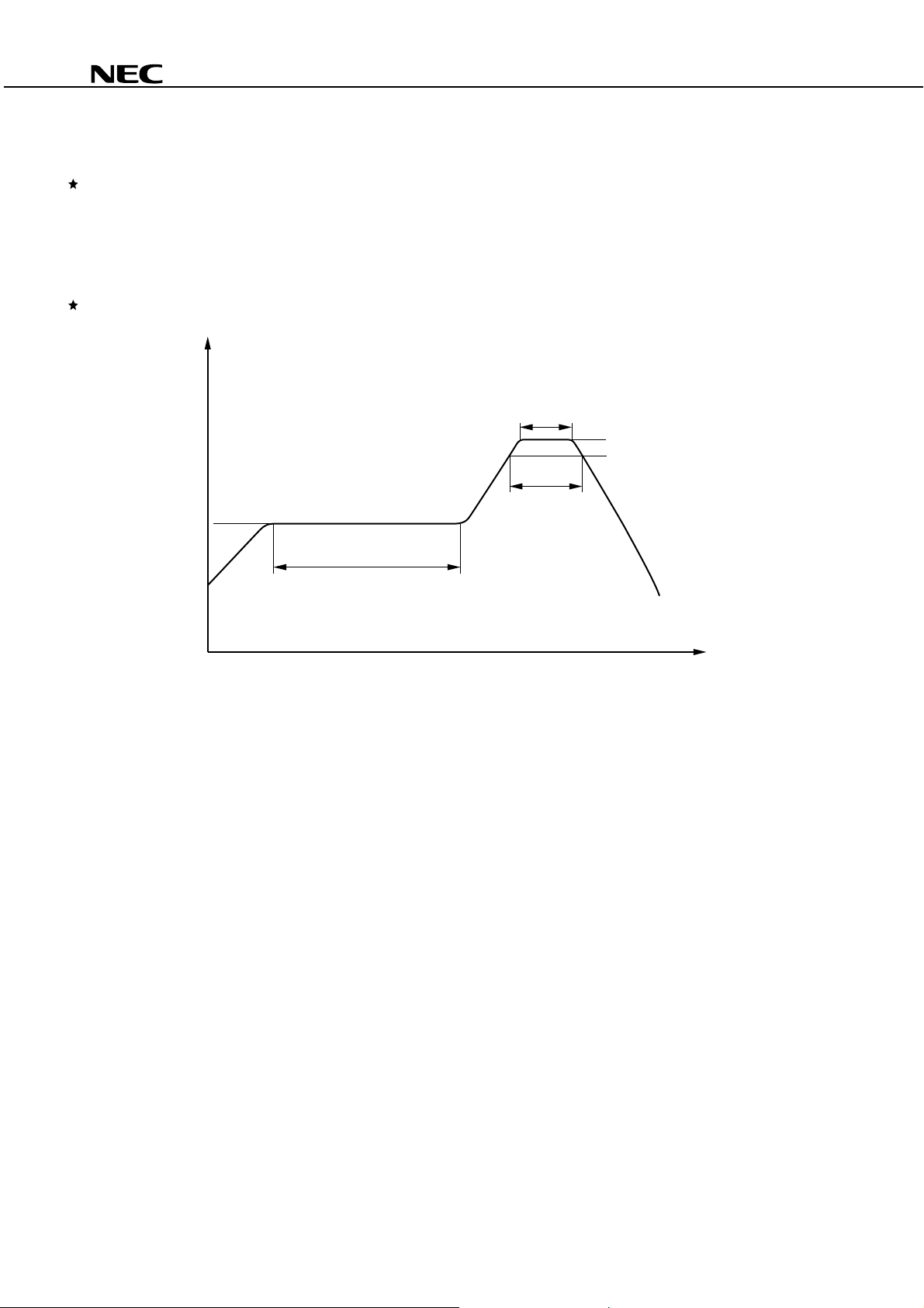
Recommended Temperature Profile of Infrared Reflow
(heating)
to 10 s
235 ˚C (peak temperature)
210 ˚C
to 30 s
100 to 160 ˚C
PS9711
60 to 120 s
(preheating)
Package Surface Temperature T (˚C)
Time (s)
(2) Dip soldering
• Temperature 260 °C or below (molten solder temperature)
• Time 10 seconds or less
• Number of times One (Allowed to be dipped in solder including plastic mold portion.)
• Flux Rosin flux containing small amount of chlorine (The flux with a maximum chlorine content of
0.2 Wt % is recommended.)
(3) Cautions
•Fluxes
Avoid removing the residual flux with freon-based and chlorine-based cleaning solvent.
10
Data Sheet P13103EJ3V0DS00

[MEMO]
PS9711
Data Sheet P13103EJ3V0DS00
11

PS9711
CAUTION
Within this device there exists GaAs (Gallium Arsenide) material which is a
harmful substance if ingested. Please do not under any circumstances break the
hermetic seal.
NEPOC is a trademark of NEC Corporation.
• The information in this document is subject to change without notice. Before using this document, please
confirm that this is the latest version.
• No part of this document may be copied or reproduced in any form or by any means without the prior written
consent of NEC Corporation. NEC Corporation assumes no responsibility for any errors which may appear in
this document.
• NEC Corporation does not assume any liability for infringement of patents, copyrights or other intellectual property
rights of third parties by or arising from use of a device described herein or any other liability arising from use
of such device. No license, either express, implied or otherwise, is granted under any patents, copyrights or other
intellectual property rights of NEC Corporation or others.
• Descriptions of circuits, software, and other related information in this document are provided for illustrative
purposes in semiconductor product operation and application examples. The incorporation of these circuits,
software, and information in the design of the customer's equipment shall be done under the full responsibility
of the customer. NEC Corporation assumes no responsibility for any losses incurred by the customer or third
parties arising from the use of these circuits, software, and information.
• While NEC Corporation has been making continuous effort to enhance the reliability of its semiconductor devices,
the possibility of defects cannot be eliminated entirely. To minimize risks of damage or injury to persons or
property arising from a defect in an NEC semiconductor device, customers must incorporate sufficient safety
measures in its design, such as redundancy, fire-containment, and anti-failure features.
• NEC devices are classified into the following three quality grades:
"Standard", "Special", and "Specific". The Specific quality grade applies only to devices developed based on a
customer designated "quality assurance program" for a specific application. The recommended applications of
a device depend on its quality grade, as indicated below. Customers must check the quality grade of each device
before using it in a particular application.
Standard: Computers, office equipment, communications equipment, test and measurement equipment,
audio and visual equipment, home electronic appliances, machine tools, personal electronic
equipment and industrial robots
Special: Transportation equipment (automobiles, trains, ships, etc.), traffic control systems, anti-disaster
systems, anti-crime systems, safety equipment and medical equipment (not specifically designed
for life support)
Specific: Aircraft, aerospace equipment, submersible repeaters, nuclear reactor control systems, life
support systems or medical equipment for life support, etc.
The quality grade of NEC devices is "Standard" unless otherwise specified in NEC's Data Sheets or Data Books.
If customers intend to use NEC devices for applications other than those specified for Standard quality grade,
they should contact an NEC sales representative in advance.
M7 98. 8
 Loading...