NEC UPD78P328GF-3BE Datasheet

DATA SHEET
MOS Integrated Circuit
µ
PD78P328
16/8-BIT SINGLE-CHIP MICROCONTROLLER
The µPD78P328 is a product provided by replacing the µPD75328's internal mask ROM with one-time
PROM or EPROM.
The one-time PROM version is programmable only once and is useful for small-lot production of many
different products and early development and time-to-market of application sets.
The EPROM version is reprogrammable, and suited for the evaluation of systems.
Functions are described in detail in the following user's manual. Be sure to read it before designing.
µ
PD78328 User's Manual: IEU-1268
FEATURES
•
µ
PD78328 compatible
• For mass-production, the µPD78P328 can be replaced with the µPD78328 incorporating mask ROM
• Internal PROM: 16,384 x 8 bits
• Programmable once only (one-time PROM version without window)
• Erasable with ultraviolet rays and electrically programmable (EPROM version with window)
• PROM programming characteristics:
• The µPD78P328 is a QTOP
Remark QTOP microcontroller is a general term for microcontrollers which incorporates one-time PROM, and
are totally supported by NEC's programming service (from programming to marking, screening, and
verification).
ORDERING INFORMATION
Part Number Package Internal ROM
µ
PD78P328CW 64-pin plastic shrink DIP (750 mils) One-time PROM
µ
PD78P328GF-3BE 64-pin plastic QFP (14 x 20 mm) One-time PROM
µ
PD78P328DW 64-pin ceramic shrink DIP (750 mils) (with window) EPROM
TM
microcontroller.
µ
PD27C256A compatible
Functions common to the one-time PROM and EPROM versions are referred to as PROM functions throughout this document.
Document No. U10209EJ4V0DS00 (4th edition)
(Previous No. IC-2486)
Date Published October 1995 P
Printed in Japan
The information in this document is subject to change without notice.
The mark
shows revised points.
*
NEC Corporation
1990
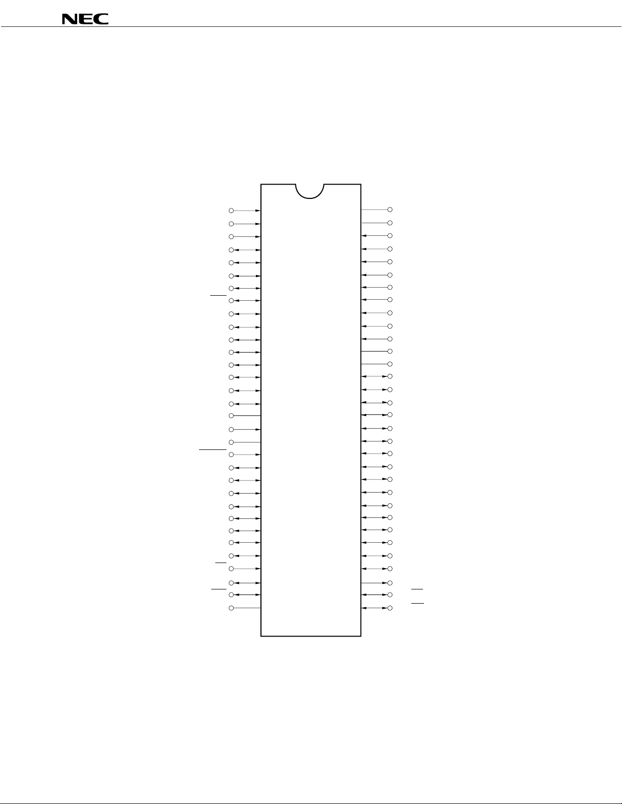
PIN CONFIGURATIONS
(1) Normal operating mode
• 64-pin plastic shrink DIP (750 mils)
µ
PD78P328CW
• 64-pin ceramic shrink DIP (750 mils) (with window)
µ
PD78P328DW
µ
PD78P328
P20/NM1
P21/INTP0
P22/INTP1
P30/TxD
P31/RxD
P32/SO/SB0
P33/SI/SB1
P34/SCK
P80/TO0
P81/TO1
P82/TO2
P83/TO3
P84/TO4
P85/TO5
P86/TO6/INTP2
P87/TO7/PWM
V
X1
X2
RESET
P00/RTP0
P01/RTP1
P02/RTP2
P03/RTP3
P04/RTP4
P05/RTP5
P06/RTP6
P07/RTP7
EA
P93/TMD
P92/TAS
V
1
2
3
4
5
6
7
8
9
10
11
12
13
14
15
16
SS
SS
17
18
19
20
21
22
23
24
25
26
27
28
29
30
31
32
64
63
62
61
60
59
58
57
56
55
54
53
52
51
50
49
48
47
46
45
44
43
42
41
40
39
38
37
36
35
34
33
V
DD
AVDD
AVREF
P77/ANI7
P76/ANI6
P75/ANI5
P74/ANI4
P73/ANI3
P72/ANI2
P71/ANI1
P70/ANI0
AV
SS
VDD
P57/A15
P56/A14
P55/A13
P54/A12
P53/A11
P52/A10
P51/A9
P50/A8
P47/AD7
P46/AD6
P45/AD5
P44/AD4
P43/AD3
P42/AD2
P41/AD1
P40/AD0
ASTB
P90/RD
P91/WR
Remark These pins are compatible with the
2
µ
PD78328CW pins.
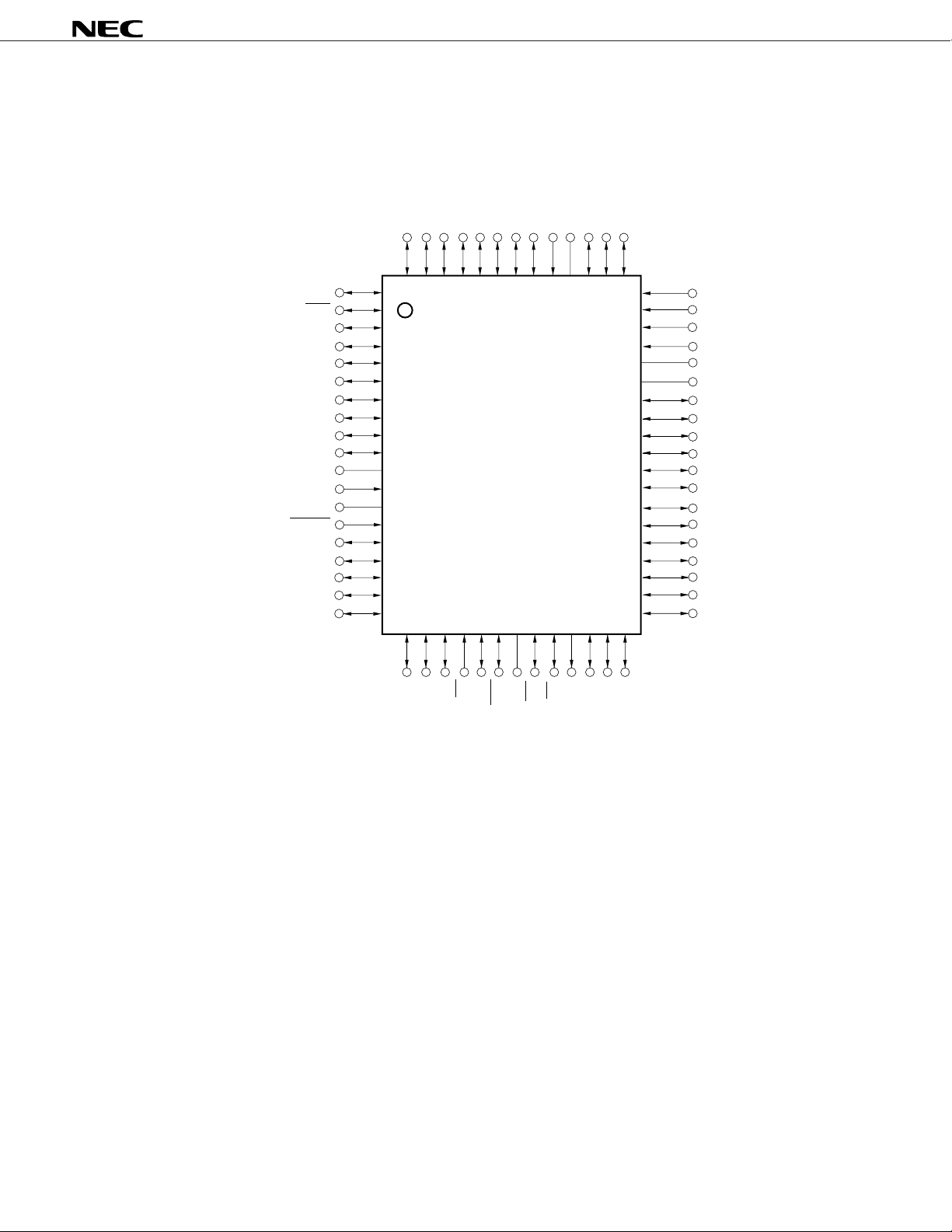
• 64-pin plastic QFP (14 x 20 mm)
µ
PD78P328GF-3BE
P33/SI/SB1
P34/SCK
P80/TO0
P81/TO1
P82/TO2
P83TO3
P84/TO4
P85/TO5
P86/TO6/INTP2
P87/TO7/PWM
V
SS
X1
X2
RESET
P00/RTP0
P01/RTP1
P02/RTP2
P03/RTP3
P04/RTP4
REF
P32/SO/SB0
P31/RxD
P30/RxD
P22/INTP/TI
P21/INTP0
P20/NMI
VDDAVDDAV
64 6362 61 60 59 58 57 56 55 54 53 52
1
2
3
4
5
6
7
8
9
10
11
12
13
14
15
16
17
18
19
20 21 22 2324 25 26 27 28 29 30 31 32
P77/ANI7
P76/ANI6
P75/ANI5
P74/ANI4
51
50
49
48
47
46
45
44
43
42
41
40
39
38
37
36
35
34
33
P73/ANI3
P72/ANI2
P71/ANI1
P70/ANI0
SS
AV
V
DD
P57/A15
P56/A14
P55/A13
P54/A12
P53/A11
P52/A10
P51/A9
P50/A8
P47/AD7
P46/AD6
P45/AD5
P44/AD4
P43/AD3
µ
PD78P328
SS
V
P92/TAS
P93/TMD
P91/WR
P05/RTP5
P06/RTP6
P07/RTP7
EA
Remark These pins are compatible with the µPD78328GF pins.
ASTB
P90/RD
P40/AD0
P41/AD1
P42/AD2
3

µ
P00-P07 : Port 0 SI : Serial Input
P20-P22 : Port 2 SO : Serial Output
P30-P34 : Port 3 SB0-SB1 : Serial Bus0-1
P40-P47 : Port 4 RD : Read Strobe
P50-P57 : Port 5 WR : Write Strobe
P70-P77 : Port 7 ASTB : Address Strobe
P80-P87 : Port 8 EA : External Access
P90-P93 : Port 9 RESET : Reset
A8-A15 : Address8-15 SCK : Serial Clock
AD0-AD7 : Address0-7/Data0-7 TAS : Turbo Access Strobe
ANI0-ANI7 : Analog Input0-7 TMD : Turbo Mode
TO0-TO7 : Timer Output0-7 X1, X2 : Crystal1, 2
NMI : Nonmaskable Interrupt AV
PWM : Pulse Wide Modulation Output AVREF : Analog Reference Voltage
INTP0-INTP2 : Interrupt From Peripherals0-2 AV
RTP0-RTP7 : Real-Time Port0-7 VDD : Power Supply
TxD : Transmit Data VSS : Ground
RxD : Receive Data
DD : Analog VDD
SS : Analog VSS
PD78P328
4
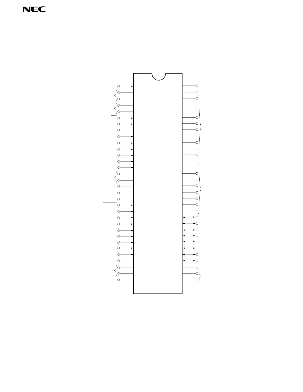
(2) PROM programming mode (RESET = H, AVDD = L)
• 64-pin plastic shrink DIP (750 mils)
µ
PD78P328CW
• 64-pin ceramic shrink DIP (750 mils) (with window)
µ
PD78P328DW
µ
PD78P328
A9
(G)
(L)
OE
CE
(L)
A8
A10
A11
A12
A13
A14
(L)
V
(G)
(Open)
RESET
A0
A1
A2
A3
A4
A5
A6
A7
V
(L)
V
1
2
3
4
5
6
7
8
9
10
11
12
13
14
15
16
SS
PP
SS
17
18
19
20
21
22
23
24
25
26
27
28
29
30
31
32
64
63
62
61
60
59
58
57
56
55
54
53
52
51
50
49
48
47
46
45
44
43
42
41
40
39
38
37
36
35
34
33
V
DD
AV
DD
(G)
DD
V
(L)
D7
D6
D5
D4
D3
D2
D1
D0
(Open)
(L)
Caution The recommended connection of the unused pins in the PROM programming mode are indicated
in parentheses.
L : Connect each pin to V
SS via a resistor.
G : Connect the pin to VSS.
Open : Leave the pin unconnected.
5
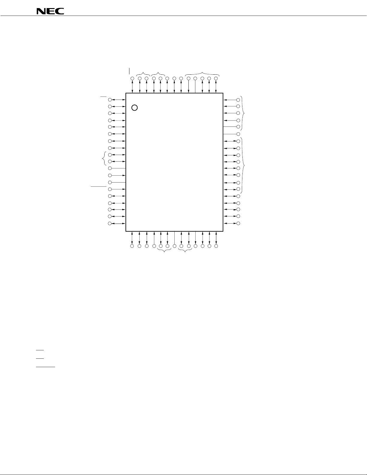
• 64-pin plastic QFP (14 x 20 mm)
µ
PD78P328GF-3BE
µ
PD78P328
CE
(L)
A8
A10
A11
A12
A13
A14
(L)
V
(G)
(Open)
RESET
A0
A1
A2
A3
A4
(L)
OE
64 63 62 61 60 59 58 57 56 55 54 53 52
1
2
3
4
5
6
7
8
9
10
SS
11
12
13
14
15
16
17
18
19
20 21 22 2324 25 26 27 2829 30 31 32
(G)
A9
DD
DD
AV
V
(G)
51
50
49
48
47
46
45
44
43
42
41
40
39
38
37
36
35
34
33
V
D7
D6
D5
D4
D3
(G)
DD
(L)
A5A6A7
PP
V
(L)
SS
V
(L)
D0D1D2
(Open)
Caution The recommended connection of the unused pins in the PROM programming mode are indicated
in parentheses.
L : Connect each pin to VSS via a resistor.
G : Connect the pin to V
SS.
Open : Leave the pin unconnected.
A0-A14 : Address0-14 AV
DD : Analog VDD
D0-D7 : Data0-7 VDD : Power Supply
CE : Chip Enable VSS : Ground
OE : Output Enable V
PP : Programming Power Supply
RESET : Reset
6
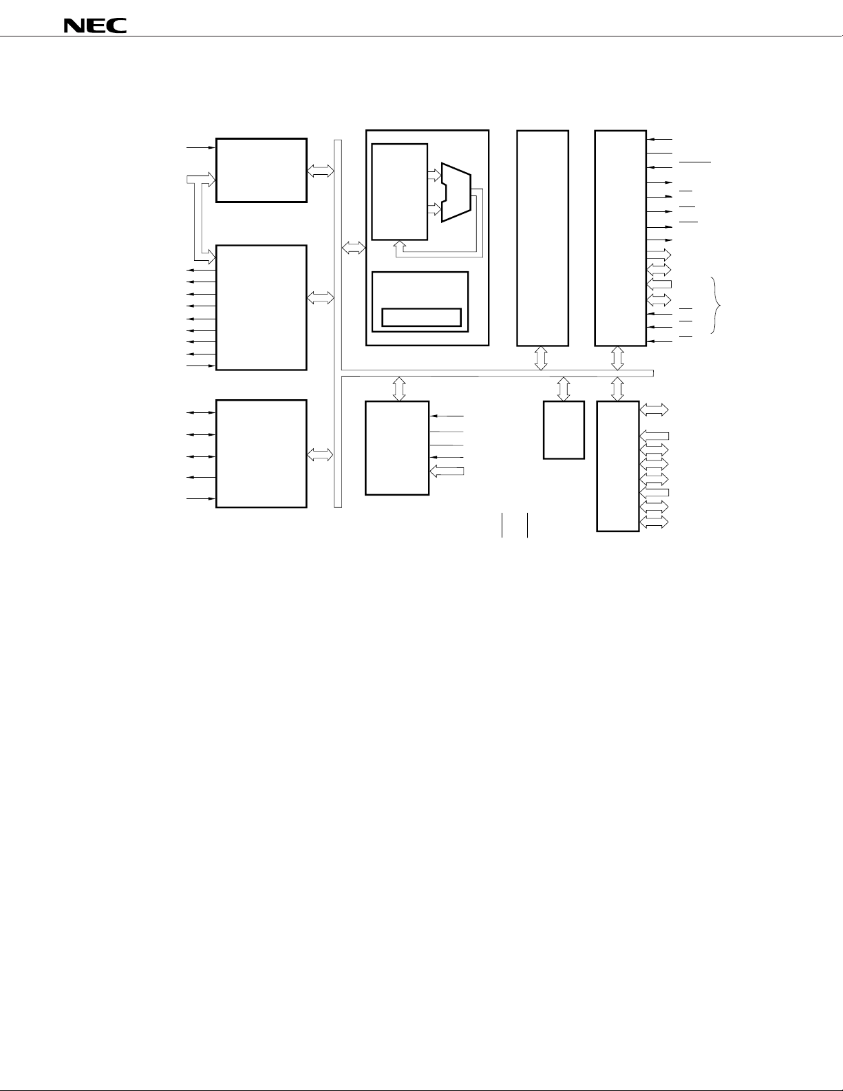
BLOCK DIAGRAM
µ
PD78P328
(P20) NMI
INTP0-INTP2
(P21, P22, P86)
(P80) TO0
(P81) TO1
(P82) TO2
(P83) TO3
(P84) TO4
(P85) TO5
(P86) TO6
(P87) TO7/PWM
(P22) TI/INTP1
(P34) SCK
(P32) SO/SB0
(P33) SI/SB1
(P30) TxD
(P31) RxD
Programmable
Interrupt
Controller
Timer/Counter Unit
(Real-Time
Pulse Unit)
Serial Interface
(SBI)
(UART)
Main RAM
General
Registers
128 x 8
&
Data
Memory
128 x 8
Micro Sequence
Control
Micro ROM
A/D Converter
(10-bit)
EXU PROM/RAM
ALU
PROM
16K x 8
&
Peripheral
RAM
256 X 8
REF
AV
AV
AV
SS
DD
WDT
INTP0
ANI0-ANI7
(P70-P77)
/
/
2
2
DD
SS
V
V
BCU
System
Control
&
Bus
Control
&
Prefetch
Control
Ports
X1
X2
RESET
ASTB
RD (P90)
WR (P91)
TAS (P92)
TMD (P93)
A8-A15 (P50-P57)
AD0-AD7 (P40-P47)
A0-A14
D0-D7
CE
Note
OE
Note
EA/V
PP
P00-P07
(Real-Time Port)
P20-P22
P30-P34
P40-P47
P50-P57
P70-P77
P80-P87
P90-P93
Note During PROM programming mode
7

CONTENTS
1. PIN FUNCTIONS ... 9
1.1 Normal Operating Mode ... 9
1.2 PROM Programming Mode (RESET = H, AVDD = L) ... 11
1.3 Pin Input/Output Circuits and Recommended Connection of Unused Pins ... 12
2. DIFFERENCES BETWEEN µPD78P328 and µPD78328 ... 14
3. PROM PROGRAMMING ... 15
3.1 Operation Mode ... 15
3.2 PROM Write Procedure ... 16
3.3 PROM Read Procedure ... 18
4. ERASURE CHARACTERISTICS (EPROM VERSION ONLY) ... 19
5. WINDOW SEAL (EPROM VERSION ONLY) ... 19
µ
PD78P328
6. ONE-TIME PROM VERSION SCREENING ... 19
7. ELECTRICAL SPECIFICATIONS ... 20
8. PACKAGE DRAWINGS ... 35
9. RECOMMENDED SOLDERING CONDITIONS ... 37
APPENDIX A. DRAWINGS OF CONVERSION SOCKET AND RECOMMENDED FOOTPRINT... 38
APPENDIX B. TOOLS ... 40
B.1 Development Tools ... 40
B.2 Evaluation Tools ... 43
B.3 Embedded Software ... 43
*
8

µ
PD78P328
1. PIN FUNCTIONS
1.1 Normal Operating Mode
(1) Port Pins
Pin Name Input/Output Function Alternate
Function
P00-P07 Input/Output PORT0 RTP0-RTP7
4-/8-bit input/output port
Input or output mode can be specified bit-wise.
The port can also operate as a real-time output port.
P20 Input PORT 2 NMI
P21 3-bit input-only port INTP0
P22 INTP1/TI
P30 Input/Output PORT 3 TxD
P31 5-bit input/output port RxD
P32 Input or output mode can be specified bit-wise. SO/SB0
P33 SI/SB1
P34 SCK
P40-P47 Input/Output PORT 4 AD0-AD7
8-bit input/output port
Input or output mode can be specified in 8-bit units.
P50-P57 Input/Output PORT 5 A8-A15
8-bit input/output port
Input or output mode can be specified bit-wise.
P70-P77 Input PORT 7 ANI0-ANI7
8-bit input-only port
P80 Input/Output PORT 8 TO0
P81 8-bit input/output port TO1
P82 Input or output mode can be specified bit-wise. TO2
P83 TO3
P84 TO4
P85 TO5
P86 TO6/INTP2
P87 TO7/PWM
P90 Input/Output PORT 9 RD
P91 4-bit input/output port WR
P92 Input or output mode can be specified bit-wise. TAS
P93 TMD
9

(2) Non-Port Pins (1/2)
Pin Name Input/Output Function Alternate
RTP0-RTP7 Output Real-time output port which outputs a pulse in synchronization with the trigger signal from P00-P07
NMI Input Edge-detected nonmaskable interrupt request input. P20
INTP0 Input Edge-detected external interrupt request input. P21
INTP1 The valid edge can be specified in the mode register. P22/T1
INTP2 P86/TO6
TI Input External count clock input pin to timer 1 (TM1). S22/INTP1
RxD Input Serial data input pin to asynchronous serial interface (UART). P30
TxD Output Serial data output pin from asynchronous serial interface (UART). P31
SO Output Serial data output pin from clocked serial interface in 3-wire mode. P32/SB0
SI Input Serial data input pin to clocked serial interface in 3-wire mode. P33/SB1
SB0 Input/Output Serial data input/output pins to/from clocked serial interface in SBI mode. P32/SO
SB1 P33/SI
SCK Input/Output Serial clock input/output pin to/from clocked serial interface. P34
AD0-AD7 Input/Output Multiplexed address/data bus used when external memory is added. P40-P47
A8-A15 Output Address bus used when external memory is added. P50-P57
TO0 Output Pulse output from real-time pulse unit. P80
TO1 P81
TO2 P82
TO3 P83
TO4 P84
TO5 P85
TO6 P86/INTP2
TO7 P87/PWM
PWM Output PWM signal output from real-time pulse unit. P87/TO7
RD Output Strobe signal output for external memory read operation. P90
WR Strobe signal output for external memory write operation. P91
*
TAS Control signal output pins to access turbo access manager (µPD71P301).
TMD P93
ASTB Output Timing signal output pin to externally latch an address information output to port 4 for —
EA Input For µPD78P328, normally connect the EA pin to VDD. When the EA pin is connected to —
real-time pulse unit (RPU).
The rising or falling edge can be selected for the valid edge by setting the mode register.
Note
external memory access.
VSS, the µPD78P328 enters the ROMless mode and external memory is accessed.
The EA pin level cannot be changed during operation.
µ
PD78P328
Function
P92
Note Turbo access manager (µPD71P301) is available for maintenance purposes only.
10

µ
PD78P328
(2) Non-Port Pins (2/2)
Pin Name Input/Output Function Alternate
Function
ANI0-ANI7 Input Analog input to A/D converter. P70-P77
AVREF Input A/D converter reference voltage input. —
AVDD — A/D converter analog power supply. —
AVSS — A/D converter GND. —
RESET Input System reset input. —
X1 Input Crystal connection pin for system clock generation. To supply external clock, —
X2 — input to the X1 and input reverse signal to the X2 pin (X2 pin can be unconnected.) —
VDD — Positive power supply pin. —
VSS — GND pin. —
1.2 PROM Programming Mode (RESET = H, AVDD = L)
Pin Name Input/Output Function
AVDD Input PROM programming mode setting.
RESET
A0-A14 — Address bus.
D0-D7 — Data bus.
CE Input PROM enable to PROM.
OE Input Read strobe to PROM.
VPP — Write power supply.
VDD Positive power supply.
VSS GND.
11

1.3 Pin Input/Output Circuits and Recommended Connection of Unused Pins
Table 1-1 and Figure 1-1 show the pin input/output circuit schematically.
Table 1-1. Pin Input/Output Circuits and Recommended Connection of Unused Pins
Pin Input/Output Recommended connection of unused pins
circuit type
P00P07/RTP0-RTP7 5 Input state: Independently connect to VDD or VSS via a resistor.
Output state: Leave Open.
P21/NMI 2 Connect to VSS.
P21/INTP0
P27/INTP6/TI
P30/TxD 5 Input state: Independently connect to VDD or VSS via a resistor.
P31/RxD Output state: Leave Open.
P32/SO/SB0 8
P33/SI/SB1
P34/SCK
P40/AD0-P47/AD0-AD7 5
P50/P57/A8-A15
P70-P77/ANI0-ANI7 9 Connect to VSS.
P80-P85/TO0-TO5 5 Input state: Independently connect to VDD or VSS via a resistor.
P86/TO6/INTP2 6 Output state: Leave Open.
P87/TO7/PWM 5
P90/RD 5
P91/WR
P92/TAS
P93/TMD
ASTB 4 Leave Open.
EA 1 —
RESET 2 —
AVREF, AVSS — Connect to V SS.
VDD — Connect to VDD.
µ
PD78P328
12
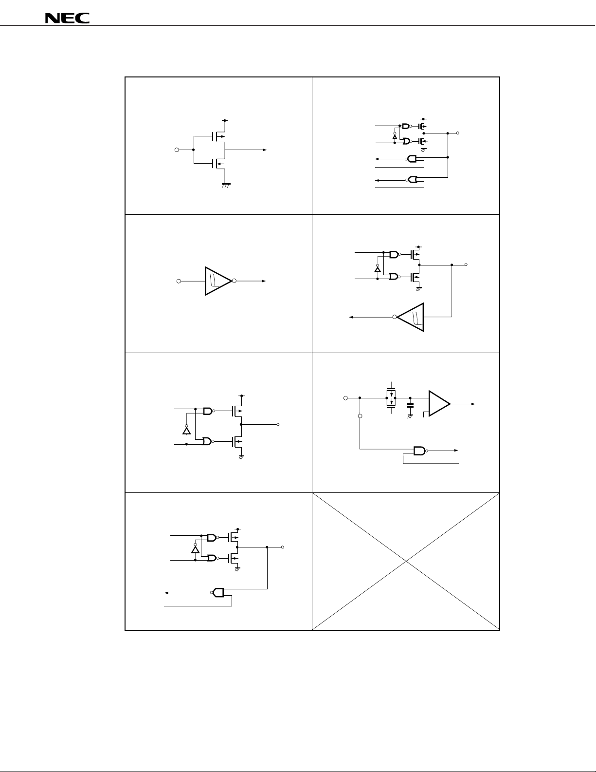
Figure 1-1. Pin Input/Output Circuits
TYPE 1 TYPE 6
V
DD
IN
P-ch
N-ch
data input enable
control signal
control input
enable
data
output
disable
data
µ
PD78P328
V
DD
P-ch
IN/OUT
N-ch
TYPE 2
TYPE 8
data
IN
output
disable
Schmitt-triggerred input with hysteresis characteristics
TYPE 4 TYPE 9
V
DD
IN
data
output
disable
Push-pull output that can be placed in high impedance
(both P-ch and N-ch off).
P-ch
N-ch
OUT
TYPE 5
V
P-ch
N-ch
(Threshold voltage)
DD
V
P-ch
N-ch
REF
IN/OUT
Comparator
+
–
input
enable
data
output
disable
input
disable
V
DD
P-ch
IN/OUT
N-ch
13

µ
PD78P328
2. DIFFERENCES BETWEEN µPD78P328 and µPD78328
The µPD78P328 is a product provided by replacing the µPD78328's on-chip mask ROM with one-time PROM
or EPROM. Thus, the µPD78P328 and µPD78328 are the same in function except for the ROM specifications such
as write or verify. Table 2-1 lists the differences between these two products.
µ
This Data Sheet describes the PROM specification function. Refer to the
other functions.
PD78328 documents for details of
Table 2-1. Differences between µPD78P328 and µPD78328
Item
Internal program memory One-time PROM EPROM Mask ROM
(electrical program) (programmable only once) (reprogrammable) (nonprogrammable)
PROM programming pin Contained Not contained
Package • 64-pin plastic shrink DIP • 64-pin ceramic shrink DIP • 64-pin plastic shrink DIP
*
Electrical specifications Current dissipations are different.
Others Noise immunity and noise radiation differ because circuit complexity and mask layout are
*
Caution The noise immunity and noise radiation differ between the PROM and mask ROM versions. To
*
replace the PROM version with the mask ROM version when shifting from experimental production
to mass production, evaluate your system by using the CS version (not ES version) of the mask
ROM version.
µ
PD78P328
• 64-pin plastic QFP (with window) • 64-pin plastic QFP
different.
µ
PD78328
14

µ
PD78P328
3. PROM PROGRAMMING
The PROM incorporated in the µPD78P328 is a 16,384 x 8-bit electrically writable PROM. For programming,
set the PROM programming mode by using the RESET and AVDD pins.
The programming characteristics are compatible with the µPD27C256A programming characteristics.
Table 3-1. Pin Function in Programming Mode
Function Normal Operating Mode Programming Mode
Address input P00-P07, P80, P20, P81-P85 A0-A14
Data input P40-P47 D0-D7
Chip enable/program pulse P33 CE
Output enable P32 OE
Program voltage EA VPP
Mode control RESET, AVDD
3.1 Operation Mode
To set the program write/verify mode, set RESET = H and AV
selected by setting the CE and OE pins, as listed in Table 3-2.
To read the PROM contents, set the read mode.
Connect the unused pins exactly as indicated on Pin Configuration.
DD = L. For the mode, the operation mode can be
Table 3-2. PROM Programming Operation Mode
Mode RESET AVDD CE OE VPP VDD D0-D7
Program write H L L H +12.5 V +6 V Data input
Program verify H L Data output
Program inhibit H H High impedance
Read L L +5 V +5 V Data output
Output disable L H High impedance
Standby H L/H High impedance
Caution When VPP is set to +12.5 V and VDD is set to +6V, setting both CE and OE to L is inhibited.
15
 Loading...