


User’s Manual
µ
PD78078, 78078Y Subseries
8-bit Single-chip Microcontrollers
µ
PD78076
µ
PD78078
µ
PD78P078
µ
PD78076Y
µ
PD78078Y
µ
PD78P078Y
Document No. U10641EJ4V0UM00 (4th edition)
Date Published December 1997 N
©
Printed in Japan
1994

[MEMO]
2

NOTES FOR CMOS DEVICES
1 PRECAUTION AGAINST ESD FOR SEMICONDUCTORS
Note:
Strong electric field, when exposed to a MOS device, can cause destruction of the gate oxide and
ultimately degrade the device operation. Steps must be taken to stop generation of static electricity
as much as possible, and quickly dissipate it once, when it has occurred. Environmental control
must be adequate. When it is dry, humidifier should be used. It is recommended to avoid using
insulators that easily build static electricity. Semiconductor devices must be stored and transported
in an anti-static container, static shielding bag or conductive material. All test and measurement
tools including work bench and floor should be grounded. The operator should be grounded using
wrist strap. Semiconductor devices must not be touched with bare hands. Similar precautions need
to be taken for PW boards with semiconductor devices on it.
2 HANDLING OF UNUSED INPUT PINS FOR CMOS
Note:
No connection for CMOS device inputs can be cause of malfunction. If no connection is provided
to the input pins, it is possible that an internal input level may be generated due to noise, etc., hence
causing malfunction. CMOS devices behave differently than Bipolar or NMOS devices. Input levels
of CMOS devices must be fixed high or low by using a pull-up or pull-down circuitry. Each unused
pin should be connected to V
being an output pin. All handling related to the unused pins must be judged device by device and
related specifications governing the devices.
DD or GND with a resistor, if it is considered to have a possibility of
3 STATUS BEFORE INITIALIZATION OF MOS DEVICES
Note:
Power-on does not necessarily define initial status of MOS device. Production process of MOS
does not define the initial operation status of the device. Immediately after the power source is
turned ON, the devices with reset function have not yet been initialized. Hence, power-on does
not guarantee out-pin levels, I/O settings or contents of registers. Device is not initialized until the
reset signal is received. Reset operation must be executed immediately after power-on for devices
having reset function.
FIP, EEPROM, IEBus, and QTOP are trademarks of NEC Corporation.
MS-DOS, Windows, and WindowsNT are either registered trademarks or trademarks of Microsoft
Corporation in the United States and/or other countries.
IBM DOS, IBM PC/AT, and PC DOS are trademarks of International Business Machines Corporation.
HP9000 Series 700 and HP-UX are trademarks of Hewlett-Packard Company.
SPARCstation is a trademark of SPARC International, Inc.
SunOS is a trademark of Sun Microsystems, Inc.
Ethernet is a trademark of XEROX Corporation.
OSF/Motif is a trademark of Open Software Foundation, Inc.
NEWS and NEWS-OS are trademarks of Sony Corporation.
TRON is an abbreviation of The Realtime Operating System Nucleus.
ITRON is an abbreviation of Industrial TRON.
3

The export of these products from Japan is regulated by the Japanese government. The export of some or all of
these products may be prohibited without governmental license. To export or re-export some or all of these products
from a country other than Japan may also be prohibited without a license from that country. Please call an NEC
sales representative.
License not needed:
The customer must judge the need for license:
The application circuits and their parameters are for reference only and are not intended for use in actual design-ins.
µ
PD78P078KL-T, 78P078YKL-T
µ
PD78076GC-xxx-7EA, 78076GC-xxx-8EU, 78076GF-xxx-3BA,
µ
PD78076YGF-xxx-3BA
µ
PD78078GC-xxx-7EA, 78078GC-xxx-8EU, 78078GF-xxx-3BA,
µ
PD78078YGF-xxx-3BA
µ
PD78P078GC-7EA, 78P078GC-8EU, 78P078GF-3BA, 78P078YGF-3BA
Purchase of NEC I2C components conveys a license under the Philips I2C Patent Rights to use these
components in an I
2
C system, provided that the system conforms to the I2C Standard Specification as
defined by Philips.
The information in this document is subject to change without notice.
No part of this document may be copied or reproduced in any form or by any means without the prior written consent
of NEC Corporation. NEC Corporation assumes no responsibility for any errors which may appear in this
document.
NEC Corporation does not assume any liability for infringement of patents, copyrights or other intellectual property
rights of third parties by or arising from use of a device described herein or any other liability arising from use of
such device. No license, either express, implied or otherwise, is granted under any patents, copyrights or other
intellectual property rights of NEC Corporation or others.
While NEC Corporation has been making continuous effort to enhance the reliability of its semiconductor devices,
the possibility of defects cannot be eliminated entirely. To minimize risks of damage or injury to persons or property
arising from a defect in an NEC semiconductor device, customers must incorporate sufficient safety measures in
its design, such as redundancy, fire-containment, and anti-failure features.
NEC devices are classified into the following three quality grades:
“Standard”, “Special”, and “Specific”. The Specific quality grade applies only to devices developed based on a
customer designated “quality assurance program” for a specific application. The recommended applications of
a device depend on its quality grade, as indicated below. Customers must check the quality grade of each device
before using it in a particular application.
Standard: Computers, office equipment, communications equipment, test and measurement equipment, audio
and visual equipment, home electronic appliances, machine tools, personal electronic equipment
and industrial robots
Special: Transportation equipment (automobiles, trains, ships, etc.), traffic control systems, anti-disaster
systems, anti-crime systems, safety equipment and medical equipment (not specifically designed for
life support)
Specific: Aircrafts, aerospace equipment, submersible repeaters, nuclear reactor control systems, life support
systems or medical equipment for life support, etc.
The quality grade of NEC devices is “Standard” unless otherwise specified in NEC’s Data Sheets or Data Books.
If customers intend to use NEC devices for applications other than those specified for Standard quality grade, they
should contact an NEC sales representative in advance.
Anti-radioactive design is not implemented in this product.
M7 96.5
4

Regional Information
Some information contained in this document may vary from country to country. Before using any NEC
product in your application, please contact the NEC office in your country to obtain a list of authorized
representatives and distributors. They will verify:
• Device availability
• Ordering information
• Product release schedule
• Availability of related technical literature
• Development environment specifications (for example, specifications for third-party tools and
components, host computers, power plugs, AC supply voltages, and so forth)
• Network requirements
In addition, trademarks, registered trademarks, export restrictions, and other legal issues may also vary
from country to country.
NEC Electronics Inc. (U.S.)
Santa Clara, California
Tel: 408-588-6000
800-366-9782
Fax: 408-588-6130
800-729-9288
NEC Electronics (Germany) GmbH
Duesseldorf, Germany
Tel: 0211-65 03 02
Fax: 0211-65 03 490
NEC Electronics (UK) Ltd.
Milton Keynes, UK
Tel: 01908-691-133
Fax: 01908-670-290
NEC Electronics Italiana s.r.1.
Milano, Italy
Tel: 02-66 75 41
Fax: 02-66 75 42 99
NEC Electronics (Germany) GmbH
Benelux Office
Eindhoven, The Netherlands
Tel:040-2445845
Fax: 040-2444580
NEC Electronics (France) S.A.
Velizy-Villacoublay, France
Tel:01-30-67 58 00
Fax: 01-30-67 58 99
NEC Electronics (France) S.A.
Spain Office
Madrid, Spain
Tel: 01-504-2787
Fax: 01-504-2860
NEC Electronics (Germany) GmbH
Scandinavia Office
Taeby, Sweden
Tel: 08-63 80 820
Fax: 08-63 80 388
NEC Electronics Hong Kong Ltd.
Hong Kong
Tel:2886-9318
Fax: 2886-9022/9044
NEC Electronics Hong Kong Ltd.
Seoul Branch
Seoul, Korea
Tel: 02-528-0303
Fax: 02-528-4411
NEC Electronics Singapore Pte. Ltd.
United Square, Singapore 1130
Tel:253-8311
Fax: 250-3583
NEC Electronics Taiwan Ltd.
Taipei, Taiwan
Tel: 02-719-2377
Fax: 02-719-5951
NEC do Brasil S.A.
Cumbica-Guarulhos-SP, Brasil
Tel: 011-6465-6810
Fax: 011-6465-6829
J97. 8
5

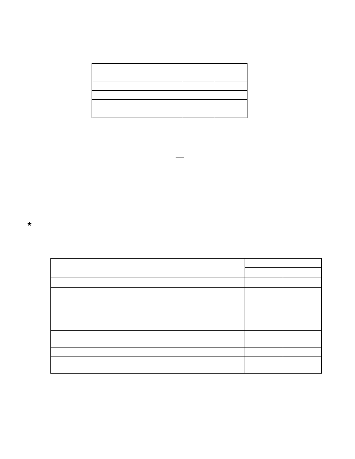
Major Revisions in This Edition
Page Description
Throughout The following products have been changed from “under development” to “already developed”.
µ
PD78078Y Subseries: µPD78076Y, 78078Y, 78P078Y
The following packages have been added to the µPD78078Y Subseries.
100-pin plastic LQFP (Fine pitch) (14 × 14 mm, resin thickness 1.4 mm)
p. 139 to 143, Block diagrams of ports have been changed.
149, 153 Figure 6-5. Block Diagram of P20, P21, P23 to P26, Figure 6-6. Block Diagram of P22 and P27,
Figure 6-7. Block Diagram of P20, P21, P23 to P26, Figure 6-8. Block Diagram of P22 and P27,
Figure 6-9. Block Diagram of P30 to P37, Figure 6-16. Block Diagram of P71 and P72,
Figure 6-20. Block Diagram of P100 and P101
p. 169 Table 7-2. Relationship between CPU Clock and Minimum Instruction Execution Time has been
added.
p. 181 8.1 Outline of Timers Incorporated into µPD78078, 78078Y Subseries has been added.
p. 241 Figure 9-10. Square Wave Output Operation Timing has been added.
p. 262 Figure 10-13. Square Wave Output Operation Timing has been added.
p. 277 Figure 12-1. Block Diagram of Watchdog Timer has been corrected.
p. 316, 366 Precautions have been added to 17.1, 18.1 Serial Interface Channel 0 Functions.
p. 323, 374 Precautions have been added to 17.3 (2), 18.3 (2) Serial Operating Mode Register 0 (CSIM0).
p. 372 Note about the BSYE flag in Figure 17-5. Serial Bus Interface Control Register Format has been
changed.
p. 336 Precautions have been added to 17.4.3 (2) (a) Bus release signal (REL), (b) Command signal
(CMD).
p. 449 19.4.3 (3) (d) Busy control option, (e) Busy & strobe control option, and (f) Bit slippage
detection function have been changed to (4) Synchronization control, and the explanation has
been improved.
p. 481 20.4.2 (2) (d) Reception
Conditions of INTSR generation when receive error occurrs has been corrected.
p. 482 Figure 20-10. Receive Error Timing has been corrected, and note has been added.
p. 490 20.4.3 (3) MSB/LSB switching as the start bit has been added.
p. 491 20.4.4 Restrictions on using UART mode has been added.
p. 569 Precautions have been added to Table 27-1. Differences between µPD78P078, 78P078Y and Mask
ROM Versions.
p. 597 APPENDIX A DIFFERENCES BETWEEN µPD78078, 78075B SUBSERIES AND µPD78070A has
been added.
p. 599 to 612 APPENDIX B DEVELOPMENT TOOL
Entirely revised: Supports in-circuit emulator IE-78K0-NS
p. 613, 614 APPENDIX C EMBEDDED SOFTWARE
Entirely revised: Fuzzy inference developing support system has been deleted.
The mark shows major revised points.
6

INTRODUCTION
Readers This manual has been prepared for user engineers who understand the functions
of the
µ
PD78078 and 78078Y Subseries and design and develop its application
systems and programs.
The µPD78078 and 78078Y Subseries consist of the following members.
• µPD78078 Subseries: µPD78076, 78078, 78P078
µ
PD78078Y Subseries: µPD78076Y, 78078Y, 78P078Y
•
Caution Of the above members, the following devices with the suffix
KL-T should be used only for experiment or function evaluation,
because they are not intended for use in equipment that will be
mass-produced and do not have enough reliability.
• µPD78P078KL-T and 78P078YKL-T
Purpose This manual is intended for users to understand the functions described in the
Organization below.
Organization The
How to Read This Manual Before reading this manual, you should have general knowledge of electric and
µ
PD78078 and 78078Y Subseries manual is separated into two parts: this
manual and the instructions edition (common to the 78K/0 Series).
µ
PD78078, 78078Y Subseries 78K/0 Series
User’s Manual User’s Manual
(This manual) — Instructions —
• Pin functions • CPU functions
• Internal block functions • Instruction set
• Interrupt • Explanation of each instruction
• Other on-chip peripheral functions
logic circuits and microcontroller.
When you want to understand the functions in general:
→ Read this manual in the order of the contents.
How to interpret the register format:
→
For the circled bit number, the bit name is defined as a reserved word in RA78K/
0, and in CC78K/0, already defined in the header file named sfrbit.h.
When you know a register name and want to confirm its details:
→ Read “APPENDIX D REGISTER INDEX”
To know the differences between the µPD78054 and 78054Y Subseries:
µ
→ See sections 1.10 and 2.10, titled “Differences with
and “Differences with
To know the µPD78078 and 78078Y Subseries instruction function in detail:
→ Refer to “78K/0 Series User’s Manual—Instructions (U12326E)”
To know the application example of each function of the µPD78078 and 78078Y
Subseries:
→ Refer to separately available Application Note.
µ
PD78054Y Subseries”, respectively.
PD78054 Subseries”
7

Chapter Organization: This manual divides the descriptions for the µPD78078 and 78078Y Subseries into different
chapters as shown below. Read only the chapters related to the device you use.
Chapter
Chapter 1 Outline (µPD78078 Subseries) √ —
Chapter 2 Outline (µPD78078Y Subseries) — √
Chapter 3 Pin Function (µPD78078 Subseries) √ —
Chapter 4 Pin Function (µPD78078Y Subseries) — √
Chapter 5 CPU Architecture √√
Chapter 6 Port Functions √√
Chapter 7 Clock Generator √√
Chapter 8 16-Bit Timer/Event Counter √√
Chapter 9 8-Bit Timer/Event Counters 1 and 2 √√
Chapter 10 8-Bit Timer/Event Counters 5 and 6 √√
Chapter 11 Watch Timer √√
Chapter 12 Watchdog Timer √√
Chapter 13 Clock Output Control Circuit √√
Chapter 14 Buzzer Output Control Circuit √√
Chapter 15 A/D Converter √√
µ
PD78078µPD78078Y
Subseries Subseries
Chapter 16 D/A Converter √√
Chapter 17 Serial Interface Channel 0 (µPD78078 Subseries) √ —
Chapter 18 Serial Interface Channel 0 (µPD78078Y Subseries) — √
Chapter 19 Serial Interface Channel 1 √√
Chapter 20 Serial Interface Channel 2 √√
Chapter 21 Real-Time Output Port √√
Chapter 22 Interrupt and Test Functions √√
Chapter 23 External Device Expansion Function √√
Chapter 24 Standby Function √√
Chapter 25 Reset Function √√
Chapter 26 ROM Correction √√
Chapter 27µPD78P078, µPD78P078Y √√
Chapter 28 Instruction Set √√
8
Differences between µPD78078 and µPD78078Y Subseries
The µPD78078 and µPD78078Y Subseries are different in the following functions of the serial
interface channel 0.
Mode of serial interface channel 0
3-wire serial I/O mode √√
2-wire serial I/O mode √√
SBI (serial bus interface) mode √ —
I2C (Inter IC) bus mode — √
√ : Supported
— : Not supported
µ
PD78078µPD78078Y
Subseries Subseries
Legend Data significance : High digits on the left and low digits on the right
Active low representations : xxx (line over the pin and signal names)
Note : Description of note in the text
Caution : Information requiring particular attention
Remark : Additional explanatory material
Numeral representations : Binary ... xxxx or xxxxB
Decimal ... xxxx
Hexadecimal ... xxxxH
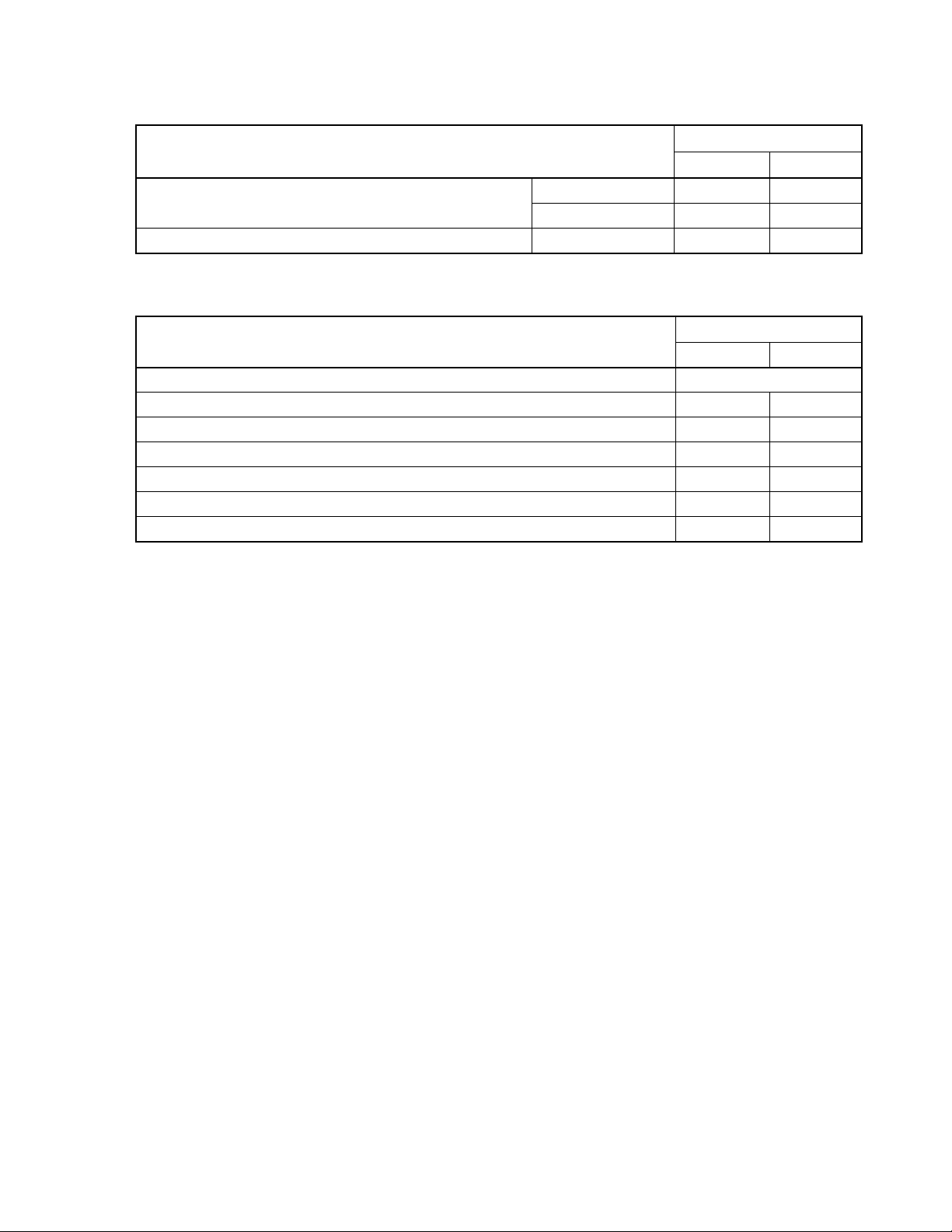
Related Documents The related documents indicated in this publication may include preliminary
versions. However, preliminary versions are not marked as such.
• Related documents for this subseries
Document name Document No.
English Japanese
µ
PD78078, 78078Y Subseries User’s Manual This manual U10641J
µ
PD78076, 78078 Data Sheet U10167E U10167J
µ
PD78P078 Data Sheet U10168E U10168J
µ
PD78076Y, 78078Y Data Sheet U10605E U10605J
µ
PD78P078Y Data Sheet U10606E U10606J
78K/0 Series User’s Manual—Instructions U12326E U12326J
78K/0 Series Instruction Table — U10903J
78K/0 Series Instruction Set — U10904J
µ
PD78078 Subseries Special Function Register Table — IEM-5607
µ
PD78078Y Subseries Special Function Register Table — IEM-5601
78K/0 Series Application Note Basics (III) U10182E U10182J
Caution The above documents are subject to change without prior notice. Be sure to use the latest
version when starting design.
9
• Development Tool Documents (User’s Manuals)
Document Name Document No.
English Japanese
RA78K Series Assembler Package Operation EEU-1399 EEU-809
Language EEU-1404 EEU-815
RA78K Series Structured Assembler Preprocessor EEU-1402 U12323J
RA78K0 Assembler Package Operation U11802E U11802J
Language U11801E U11801J
Structured Assembly U11789E U11789J
Language
CC78K Series C Compiler Operation EEU-1280 EEU-656
Language EEU-1284 EEU-655
CC78K0 C Compiler Operation U11517E U11517J
Language U11518E U11518J
CC78K0 C Compiler Application Note
CC78K Series Library Source File — U12322J
PG-1500 PROM Programmer EEU-1335 U11940J
PG-1500 Controller PC-9800 Series (MS-DOSTM)-Based EEU-1291 EEU-704
PG-1500 Controller IBM PC Series (PC DOSTM)-Based U10540E EEU-5008
IE-78K0-NS
IE-78001-R-A
IE-78K0-R-EX1
IE-78078-NS-EM1
Programming Know-how
EEA-1208 U13034J
To be prepared To be prepared
To be prepared To be prepared
To be prepared To be prepared
To be prepared To be prepared
IE-78078-R-EM U10775E U10775J
EP-78064 EEU-1469 EEU-934
SM78K0 System Simulator WindowsTM-Based Reference U10181E U10181J
SM78K Series System Simulator External Part User Open Interface Specifications U10092E U10092J
ID78K0-NS Integrated Debugger Reference
ID78K0 Integrated Debugger EWS Based Reference — U11151J
ID78K0 Integrated Debugger PC Based Reference U11539E U11539J
ID78K0 Integrated Debugger Windows Based Guides U11649E U11649J
To be prepared
U12900J
Caution The above documents are subject to change without prior notice. Be sure to use the latest
version when starting design.
10
• Documents for Embedded Software (User’s Manuals)
Document Name Document No.
English Japanese
78K/0 Series Real-time OS Basics U11537E U11537J
Installation U11536E U11536J
78K/0 Series OS MX78K0 Basics U12257E U12257J
• Other Documents
Document Name Document No.
English Japanese
IC Package Manual C10943X
Semiconductor Device Mounting Technology Manual C10535E C10535J
Quality Grades on NEC Semiconductor Devices C11531E C11531J
NEC Semiconductor Device Reliability/Quality Control System U10983E U10983J
Guide to Prevent Damage for Semiconductor Devices by Electrostatic Discharge (ESD) C11892E C11892J
Guide to Quality Assurance for Semiconductor Devices MEI-1202 —
Microcomputer Product Series Guide — U11416J
Caution The above documents are subject to change without prior notice. Be sure to use the latest
version when starting design.
11

[MEMO]
12

TABLE OF CONTENTS
CHAPTER 1 OUTLINE (µPD78078 SUBSERIES)................................................................................. 33
1.1 Features .................................................................................................................................. 33
1.2 Application Fields.................................................................................................................. 34
1.3 Ordering Information............................................................................................................. 3 4
1.4 Quality Grade ......................................................................................................................... 3 5
1.5 Pin Configuration (Top View)............................................................................................... 36
1.6 78K/0 Series Expansion........................................................................................................ 42
1.7 Block Diagram........................................................................................................................ 44
1.8 Outline of Function ................................................................................................................ 45
1.9 Mask Options .......................................................................................................................... 47
1.10 Differences with µPD78054 Subseries ................................................................................ 47
CHAPTER 2 OUTLINE (µPD78078Y SUBSERIES) .............................................................................. 49
2.1 Features .................................................................................................................................. 49
2.2 Application Fields.................................................................................................................. 50
2.3 Ordering Information............................................................................................................. 5 0
2.4 Quality Grade ......................................................................................................................... 5 1
2.5 Pin Configuration (Top View)............................................................................................... 52
2.6 78K/0 Series Expansion........................................................................................................ 58
2.7 Block Diagram........................................................................................................................ 60
2.8 Outline of Function ................................................................................................................ 61
2.9 Mask Options .......................................................................................................................... 63
2.10 Differences with µPD78054Y Subseries ............................................................................. 63
CHAPTER 3 PIN FUNCTION (µPD78078 SUBSERIES) ....................................................................... 65
3.1 Pin Function List .................................................................................................................... 65
3.1.1 Normal operating mode pins ...................................................................................................... 65
3.1.2 PROM programming mode pins (µPD78P078 only) ................................................................. 69
3.2 Description of Pin Functions ............................................................................................... 70
3.2.1 P00 to P07 (Port 0) .....................................................................................................................70
3.2.2 P10 to P17 (Port 1) .....................................................................................................................70
3.2.3 P20 to P27 (Port 2) .....................................................................................................................71
3.2.4 P30 to P37 (Port 3) .....................................................................................................................72
3.2.5 P40 to P47 (Port 4) .....................................................................................................................72
3.2.6 P50 to P57 (Port 5) .....................................................................................................................73
3.2.7 P60 to P67 (Port 6) .....................................................................................................................73
3.2.8 P70 to P72 (Port 7) .....................................................................................................................74
3.2.9 P80 to P87 (Port 8) .....................................................................................................................74
3.2.10 P90 to P96 (Port 9) ..................................................................................................................... 75
3.2.11 P100 to P103 (Port 10) ............................................................................................................... 75
3.2.12 P120 to P127 (Port 12) ............................................................................................................... 75
3.2.13 P130 and P131 (Port 13) ............................................................................................................ 76
3.2.14 AV
3.2.15 AV
3.2.16 AVDD ............................................................................................................................................. 76
REF0 .......................................................................................................................................... 76
REF1 .......................................................................................................................................... 76
13

3.2.17 AVSS ............................................................................................................................................. 76
3.2.18 RESET ......................................................................................................................................... 76
3.2.19 X1 and X2 .................................................................................................................................... 76
3.2.20 XT1 and XT2 ............................................................................................................................... 76
3.2.21 V
3.2.22 V
DD ............................................................................................................................................... 77
SS ................................................................................................................................................ 77
3.2.23 VPP (µPD78P078 only) ................................................................................................................ 77
3.2.24 IC (Mask ROM version only) ...................................................................................................... 77
3.3 Input/output Circuits and Recommended Connection of Unused Pins ........................ 78
CHAPTER 4 PIN FUNCTION (µPD78078Y SUBSERIES) ................................................................... 83
4.1 Pin Function List .................................................................................................................... 83
4.1.1 Normal operating mode pins ...................................................................................................... 83
4.1.2 PROM programming mode pins (µPD78P078Y only) ............................................................... 87
4.2 Description of Pin Functions ............................................................................................... 88
4.2.1 P00 to P07 (Port 0) .....................................................................................................................88
4.2.2 P10 to P17 (Port 1) .....................................................................................................................88
4.2.3 P20 to P27 (Port 2) .....................................................................................................................89
4.2.4 P30 to P37 (Port 3) .....................................................................................................................90
4.2.5 P40 to P47 (Port 4) .....................................................................................................................90
4.2.6 P50 to P57 (Port 5) .....................................................................................................................91
4.2.7 P60 to P67 (Port 6) .....................................................................................................................91
4.2.8 P70 to P72 (Port 7) .....................................................................................................................92
4.2.9 P80 to P87 (Port 8) .....................................................................................................................92
4.2.10 P90 to P96 (Port 9) ..................................................................................................................... 93
4.2.11 P100 to P103 (Port 10) ............................................................................................................... 93
4.2.12 P120 to P127 (Port 12) ............................................................................................................... 93
4.2.13 P130 and P131 (Port 13) ............................................................................................................ 94
4.2.14 AV
4.2.15 AV
REF0 .......................................................................................................................................... 94
REF1 .......................................................................................................................................... 94
4.2.16 AVDD ............................................................................................................................................. 94
4.2.17 AVSS ............................................................................................................................................. 94
4.2.18 RESET ......................................................................................................................................... 94
4.2.19 X1 and X2 .................................................................................................................................... 94
4.2.20 XT1 and XT2 ............................................................................................................................... 94
4.2.21 V
DD ............................................................................................................................................... 95
4.2.22 VSS ................................................................................................................................................ 95
4.2.23 VPP (µPD78P078Y only) .............................................................................................................. 95
4.2.24 IC (Mask ROM version only) ...................................................................................................... 95
4.3 Input/output Circuits and Recommended Connection of Unused Pins ........................ 96
CHAPTER 5 CPU ARCHITECTURE.................................................................................................... 101
5.1 Memory Spaces.................................................................................................................... 101
5.1.1 Internal program memory space .............................................................................................. 104
5.1.2 Internal data memory space ..................................................................................................... 106
5.1.3 Special function register (SFR) area........................................................................................ 10 6
5.1.4 External memory space ............................................................................................................ 10 6
5.1.5 Data memory addressing.......................................................................................................... 10 7
14

5.2 Processor Registers............................................................................................................ 11 0
5.2.1 Control registers ........................................................................................................................ 110
5.2.2 General registers....................................................................................................................... 11 3
5.2.3 Special function register (SFR) ................................................................................................ 114
5.3 Instruction Address Addressing ....................................................................................... 118
5.3.1 Relative addressing................................................................................................................... 118
5.3.2 Immediate addressing............................................................................................................... 1 19
5.3.3 Table indirect addressing..........................................................................................................120
5.3.4 Register addressing .................................................................................................................. 121
5.4 Operand Address Addressing ........................................................................................... 122
5.4.1 Implied addressing .................................................................................................................... 122
5.4.2 Register addressing .................................................................................................................. 123
5.4.3 Direct addressing ...................................................................................................................... 124
5.4.4 Short direct addressing ............................................................................................................. 125
5.4.5 Special function register (SFR) addressing .............................................................................126
5.4.6 Register indirect addressing .....................................................................................................127
5.4.7 Based addressing......................................................................................................................128
5.4.8 Based indexed addressing .......................................................................................................129
5.4.9 Stack addressing....................................................................................................................... 1 29
CHAPTER 6 PORT FUNCTIONS......................................................................................................... 131
6.1 Port Functions ...................................................................................................................... 131
6.2 Port Configuration ............................................................................................................... 136
6.2.1 Port 0 ......................................................................................................................................... 136
6.2.2 Port 1 ......................................................................................................................................... 138
6.2.3 Port 2 (µPD78078 Subseries) ................................................................................................... 139
µ
6.2.4 Port 2 (
6.2.5 Port 3 ......................................................................................................................................... 143
6.2.6 Port 4 ......................................................................................................................................... 144
6.2.7 Port 5 ......................................................................................................................................... 145
6.2.8 Port 6 ......................................................................................................................................... 146
6.2.9 Port 7 ......................................................................................................................................... 148
6.2.10 Port 8 ......................................................................................................................................... 150
6.2.11 Port 9 ......................................................................................................................................... 151
6.2.12 Port 10 .......................................................................................................................................153
6.2.13 Port 12 .......................................................................................................................................155
6.2.14 Port 13 .......................................................................................................................................156
PD78078Y Subseries) ................................................................................................ 141
6.3 Port Function Control Registers ....................................................................................... 157
6.4 Port Function Operations ................................................................................................... 163
6.4.1 Writing to input/output port ....................................................................................................... 163
6.4.2 Reading from input/output port................................................................................................. 1 63
6.4.3 Operations on input/output port................................................................................................ 16 3
6.5 Selection of Mask Option ................................................................................................... 1 64
15

CHAPTER 7 CLOCK GENERATOR .................................................................................................... 165
7.1 Clock Generator Functions ................................................................................................ 16 5
7.2 Clock Generator Configuration .......................................................................................... 166
7.3 Clock Generator Control Register ..................................................................................... 167
7.4 System Clock Oscillator ..................................................................................................... 1 71
7.4.1 Main system clock oscillator ..................................................................................................... 171
7.4.2 Subsystem clock oscillator........................................................................................................172
7.4.3 Divider........................................................................................................................................ 1 74
7.4.4 When no subsystem clocks are used ...................................................................................... 174
7.5 Clock Generator Operations .............................................................................................. 175
7.5.1 Main system clock operations .................................................................................................. 176
7.5.2 Subsystem clock operations ..................................................................................................... 177
7.6 Changing System Clock and CPU Clock Settings .......................................................... 178
7.6.1 Time required for switchover between system clock and CPU clock ..................................... 178
7.6.2 System clock and CPU clock switching procedure ................................................................. 17 9
CHAPTER 8 16-BIT TIMER/EVENT COUNTER.................................................................................. 181
8.1 Outline of Timers Incorporated into µPD78078, 78078Y Subseries............................. 181
8.2 16-Bit Timer/Event Counter Functions ............................................................................. 183
8.3 16-Bit Timer/Event Counter Configuration ...................................................................... 185
8.4 16-Bit Timer/Event Counter Control Registers ............................................................... 19 0
8.5 16-Bit Timer/Event Counter Operations ........................................................................... 1 98
8.5.1 Interval timer operations ........................................................................................................... 1 98
8.5.2 PWM output operations ............................................................................................................ 200
8.5.3 PPG output operations..............................................................................................................203
8.5.4 Pulse width measurement operations ...................................................................................... 204
8.5.5 External event counter operation ............................................................................................. 211
8.5.6 Square-wave output operation .................................................................................................213
8.5.7 One-shot pulse output operation .............................................................................................. 215
8.6 16-Bit Timer/Event Counter Operating Precautions....................................................... 219
CHAPTER 9 8-BIT TIMER/EVENT COUNTERS 1 AND 2................................................................... 223
9.1 8-Bit Timer/Event Counters 1 and 2 Functions............................................................... 2 23
9.1.1 8-bit timer/event counter mode.................................................................................................223
9.1.2 16-bit timer/event counter mode ............................................................................................... 226
9.2 8-Bit Timer/Event Counters 1 and 2 Configurations ...................................................... 22 8
9.3 8-Bit Timer/Event Counters 1 and 2 Control Registers ................................................. 231
9.4 8-Bit Timer/Event Counters 1 and 2 Operations............................................................. 236
9.4.1 8-bit timer/event counter mode.................................................................................................236
9.4.2 16-bit timer/event counter mode ............................................................................................... 242
9.5 8-Bit Timer/Event Counters 1 and 2 Precautions ........................................................... 246
16

CHAPTER 10 8-BIT TIMER/EVENT COUNTERS 5 AND 6................................................................. 249
10.1 8-Bit Timer/Event Counters 5 and 6 Functions............................................................... 2 49
10.2 8-Bit Timer/Event Counters 5 and 6 Configurations ...................................................... 25 2
10.3 8-Bit Timer/Event Counters 5 and 6 Control Registers ................................................. 254
10.4 8-Bit Timer/Event Counters 5 and 6 Operations............................................................. 259
10.4.1 Interval timer operations ........................................................................................................... 259
10.4.2 External event counter operation ............................................................................................. 261
10.4.3 Square-wave output .................................................................................................................. 262
10.4.4 PWM output operations ............................................................................................................ 2 64
10.5 8-Bit Timer/Event Counters 5 and 6 Precautions ........................................................... 267
CHAPTER 11 WATCH TIMER ............................................................................................................. 269
11.1 Watch Timer Functions....................................................................................................... 269
11.2 Watch Timer Configuration ................................................................................................ 270
11.3 Watch Timer Control Registers ......................................................................................... 27 1
11.4 Watch Timer Operations..................................................................................................... 274
11.4.1 Watch timer operation ............................................................................................................... 274
11.4.2 Interval timer operation ............................................................................................................. 274
CHAPTER 12 WATCHDOG TIMER ..................................................................................................... 275
12.1 Watchdog Timer Functions ................................................................................................ 275
12.2 Watchdog Timer Configuration ......................................................................................... 277
12.3 Watchdog Timer Control Registers .................................................................................. 278
12.4 Watchdog Timer Operations .............................................................................................. 281
12.4.1 Watchdog timer operation......................................................................................................... 281
12.4.2 Interval timer operation ............................................................................................................. 282
CHAPTER 13 CLOCK OUTPUT CONTROL CIRCUIT........................................................................ 283
13.1 Clock Output Control Circuit Functions .......................................................................... 283
13.2 Clock Output Control Circuit Configuration.................................................................... 2 84
13.3 Clock Output Function Control Registers ....................................................................... 285
CHAPTER 14 BUZZER OUTPUT CONTROL CIRCUIT ...................................................................... 289
14.1 Buzzer Output Control Circuit Functions ........................................................................ 289
14.2 Buzzer Output Control Circuit Configuration.................................................................. 289
14.3 Buzzer Output Function Control Registers ..................................................................... 290
CHAPTER 15 A/D CONVERTER ......................................................................................................... 293
15.1 A/D Converter Functions .................................................................................................... 293
15.2 A/D Converter Configuration ............................................................................................. 293
15.3 A/D Converter Control Registers ...................................................................................... 296
15.4 A/D Converter Operations .................................................................................................. 30 0
15.4.1 Basic operations of A/D converter............................................................................................ 300
15.4.2 Input voltage and conversion results ....................................................................................... 30 2
15.4.3 A/D converter operating mode.................................................................................................. 303
15.5 A/D Converter Cautions...................................................................................................... 305
17

CHAPTER 16 D/A CONVERTER ......................................................................................................... 309
16.1 D/A Converter Functions .................................................................................................... 309
16.2 D/A Converter Configuration ............................................................................................. 310
16.3 D/A Converter Control Registers ...................................................................................... 312
16.4 D/A Converter Operations .................................................................................................. 31 3
16.5 D/A Converter Cautions...................................................................................................... 314
CHAPTER 17 SERIAL INTERFACE CHANNEL 0 (µPD78078 SUBSERIES) .................................... 315
17.1 Serial Interface Channel 0 Functions ............................................................................... 316
17.2 Serial Interface Channel 0 Configuration......................................................................... 318
17.3 Serial Interface Channel 0 Control Registers.................................................................. 321
17.4 Serial Interface Channel 0 Operations ............................................................................. 328
17.4.1 Operation stop mode................................................................................................................. 328
17.4.2 3-wire serial I/O mode operation .............................................................................................. 329
17.4.3 SBI mode operation .................................................................................................................. 333
17.4.4 2-wire serial I/O mode operation .............................................................................................. 357
17.4.5 SCK0/P27 pin output manipulation .......................................................................................... 363
CHAPTER 18 SERIAL INTERFACE CHANNEL 0 (µPD78078Y Subseries) ..................................... 365
18.1 Serial Interface Channel 0 Functions ............................................................................... 366
18.2 Serial Interface Channel 0 Configuration......................................................................... 368
18.3 Serial Interface Channel 0 Control Registers.................................................................. 372
18.4 Serial Interface Channel 0 Operations ............................................................................. 380
18.4.1 Operation stop mode................................................................................................................. 380
18.4.2 3-wire serial I/O mode operation .............................................................................................. 381
18.4.3 2-wire serial I/O mode operation .............................................................................................. 385
2
18.4.4 I
18.4.5 Cautions on use of I2C bus mode ............................................................................................ 408
18.4.6 Restrictions in I2C bus mode .................................................................................................... 4 11
18.4.7 SCK0/SCL/P27 pin output manipulation .................................................................................. 413
C bus mode operation ............................................................................................................ 3 90
CHAPTER 19 SERIAL INTERFACE CHANNEL 1 .............................................................................. 415
19.1 Serial Interface Channel 1 Functions ............................................................................... 415
19.2 Serial Interface Channel 1 Configuration......................................................................... 416
19.3 Serial Interface Channel 1 Control Registers.................................................................. 418
19.4 Serial Interface Channel 1 Operations ............................................................................. 425
19.4.1 Operation stop mode................................................................................................................. 425
19.4.2 3-wire serial I/O mode operation .............................................................................................. 426
19.4.3 3-wire serial I/O mode operation with automatic transmit/receive function ........................... 429
CHAPTER 20 SERIAL INTERFACE CHANNEL 2 .............................................................................. 457
20.1 Serial Interface Channel 2 Functions ............................................................................... 457
20.2 Serial Interface Channel 2 Configuration......................................................................... 458
20.3 Serial Interface Channel 2 Control Registers.................................................................. 461
20.4 Serial Interface Channel 2 Operation ............................................................................... 469
20.4.1 Operation stop mode................................................................................................................. 469
20.4.2 Asynchronous serial interface (UART) mode .......................................................................... 471
20.4.3 3-wire serial I/O mode............................................................................................................... 4 84
20.4.4 Restrictions on using UART mode ........................................................................................... 4 91
18

CHAPTER 21 REAL-TIME OUTPUT PORT ........................................................................................ 495
21.1 Real-Time Output Port Functions ..................................................................................... 495
21.2 Real-Time Output Port Configuration............................................................................... 495
21.3 Real-Time Output Port Control Registers........................................................................ 497
CHAPTER 22 INTERRUPT FUNCTIONS ............................................................................................ 499
22.1 Interrupt Function Types .................................................................................................... 499
22.2 Interrupt Sources and Configuration................................................................................ 500
22.3 Interrupt Function Control Registers ............................................................................... 504
22.4 Interrupt Servicing Operations .......................................................................................... 513
22.4.1 Non-maskable interrupt request acknowledge operation ........................................................ 513
22.4.2 Maskable interrupt request acknowledge operation ................................................................ 516
22.4.3 Software interrupt request acknowledge operation ................................................................. 51 8
22.4.4 Multiple interrupt servicing ........................................................................................................519
22.4.5 Interrupt request reserve .......................................................................................................... 5 22
22.5 Test Functions ..................................................................................................................... 523
22.5.1 Registers controlling the test function ...................................................................................... 523
22.5.2 Test input signal acknowledge operation................................................................................. 5 25
CHAPTER 23 EXTERNAL DEVICE EXPANSION FUNCTION ........................................................... 527
23.1 External Device Expansion Functions ............................................................................. 527
23.2 External Device Expansion Function Control Register ................................................. 5 31
23.3 External Device Expansion Function Timing .................................................................. 534
23.3.1 Timings in multiplexed bus mode............................................................................................ 534
23.3.2 Timings in separate bus mode ................................................................................................ 53 9
CHAPTER 24 STANDBY FUNCTION.................................................................................................. 545
24.1 Standby Function and Configuration ............................................................................... 545
24.1.1 Standby function........................................................................................................................ 5 45
24.1.2 Standby function control register.............................................................................................. 546
24.2 Standby Function Operations............................................................................................ 5 47
24.2.1 HALT mode................................................................................................................................ 547
24.2.2 STOP mode ............................................................................................................................... 550
CHAPTER 25 RESET FUNCTION ....................................................................................................... 553
25.1 Reset Function ..................................................................................................................... 553
CHAPTER 26 ROM CORRECTION ..................................................................................................... 559
26.1 ROM Correction Functions ................................................................................................. 559
26.2 ROM Correction Configuration .......................................................................................... 559
26.3 ROM Correction Control Registers ................................................................................... 561
26.4 ROM Correction Application .............................................................................................. 562
26.5 ROM Correction Example ................................................................................................... 565
26.6 Program Execution Flow .................................................................................................... 566
26.7 Cautions on ROM Correction............................................................................................. 568
19

CHAPTER 27 µPD78P078, 78P078Y .................................................................................................. 569
27.1 Internal Memory Size Switching Register........................................................................ 570
27.2 Internal Extension RAM Size Switching Register........................................................... 571
27.3 PROM Programming............................................................................................................ 572
27.3.1 Operating modes .......................................................................................................................572
27.3.2 PROM write procedure.............................................................................................................. 574
27.3.3 PROM reading procedure ......................................................................................................... 578
27.4 Erasure Procedure (µPD78P078KL-T and 78P078YKL-T Only)..................................... 579
27.5 Opaque Film Masking Window (µPD78P078KL-T and 78P078YKL-T Only) ................ 579
27.6 Screening of One-Time PROM Versions .......................................................................... 579
CHAPTER 28 INSTRUCTION SET ...................................................................................................... 581
28.1 Legends Used in Operation List ........................................................................................ 582
28.1.1 Operand identifiers and description methods .......................................................................... 5 82
28.1.2 Description of “operation” column ............................................................................................583
28.1.3 Description of “flag operation” column ..................................................................................... 583
28.2 Operation List....................................................................................................................... 584
28.3 Instructions Listed by Addressing Type.......................................................................... 59 2
APPENDIX A DIFFERENCES BETWEEN µPD78078, 78075B SUBSERIES, AND µPD78070A...... 597
APPENDIX B DEVELOPMENT TOOLS .............................................................................................. 599
B.1 Language Processing Software ......................................................................................... 602
B.2 PROM Writing Tools............................................................................................................ 604
B.2.1 Hardware ................................................................................................................................... 6 04
B.2.2 Software.....................................................................................................................................604
B.3 Debugging Tools .................................................................................................................. 605
B.3.1 Hardware ................................................................................................................................... 6 05
B.3.2 Software.....................................................................................................................................607
B.4 OS for IBM PC ...................................................................................................................... 60 9
B.5 System Upgrading from Former-type In-circuit Emulator for 78K/0 Series
to IE-78001-R-A .................................................................................................................... 609
APPENDIX C EMBEDDED SOFTWARE ............................................................................................ 613
APPENDIX D REGISTER INDEX......................................................................................................... 615
D.1 Register Name Index ........................................................................................................... 615
D.2 Register Symbol Index........................................................................................................ 619
APPENDIX E REVISION HISTORY ..................................................................................................... 623
20

LIST OF FIGURES (1/9)
Figure No. Title Page
3-1 List of Pin Input/Output Circuits ................................................................................................... 80
4-1 List of Pin Input/Output Circuits ................................................................................................... 98
µ
5-1 Memory Map (
5-2 Memory Map (
5-3 Memory Map (µPD78P078, µPD78P078Y) ............................................................................... 10 3
5-4 Data Memory Addressing (µPD78076, 78076Y)....................................................................... 107
5-5 Data Memory Addressing (
5-6 Data Memory Addressing (µPD78P078, 78P078Y).................................................................. 109
5-7 Program Counter Configuration ................................................................................................. 110
5-8 Program Status Word Configuration .......................................................................................... 110
5-9 Stack Pointer Configuration ....................................................................................................... 112
5-10 Data to be Saved to Stack Memory ........................................................................................... 11 2
5-11 Data to be Reset from Stack Memory ....................................................................................... 1 12
5-12 General Register Configuration .................................................................................................. 113
PD78076, 78076Y) ........................................................................................... 101
µ
PD78078, 78078Y) ........................................................................................... 102
µ
PD78078, 78078Y)....................................................................... 108
6-1 Port Types ................................................................................................................................... 13 1
6-2 Block Diagram of P00 and P07.................................................................................................. 137
6-3 Block Diagram of P01 to P06..................................................................................................... 137
6-4 Block Diagram of P10 to P17..................................................................................................... 138
6-5 Block Diagram of P20, P21, P23 to P26 ................................................................................... 139
6-6 Block Diagram of P22 and P27.................................................................................................. 140
6-7 Block Diagram of P20, P21, P23 to P26 ................................................................................... 141
6-8 Block Diagram of P22 and P27.................................................................................................. 142
6-9 Block Diagram of P30 to P37..................................................................................................... 143
6-10 Block Diagram of P40 to P47 ..................................................................................................... 14 4
6-11 Block Diagram of Falling Edge Detection Circuit...................................................................... 144
6-12 Block Diagram of P50 to P57 ..................................................................................................... 14 5
6-13 Block Diagram of P60 to P63 ..................................................................................................... 14 7
6-14 Block Diagram of P64 to P67 ..................................................................................................... 14 7
6-15 Block Diagram of P70 ................................................................................................................. 1 48
6-16 Block Diagram of P71 and P72 .................................................................................................. 149
6-17 Block Diagram of P80 to P87 ..................................................................................................... 15 0
6-18 Block Diagram of P90 to P93 ..................................................................................................... 15 2
6-19 Block Diagram of P94 to P96 ..................................................................................................... 15 2
6-20 Block Diagram of P100 and P101 ............................................................................................. 153
6-21 Block Diagram of P102 and P103 ............................................................................................. 154
6-22 Block Diagram of P120 to P127 ................................................................................................. 155
6-23 Block Diagram of P130 and P131 ............................................................................................. 156
6-24 Port Mode Register Format........................................................................................................ 159
6-25 Pull-Up Resistor Option Register Format.................................................................................. 160
6-26 Memory Expansion Mode Register Format............................................................................... 161
6-27 Key Return Mode Register Format............................................................................................ 162
21

LIST OF FIGURES (2/9)
Figure No. Title Page
7-1 Block Diagram of Clock Generator ............................................................................................ 166
7-2 Subsystem Clock Feedback Resistor ........................................................................................ 167
7-3 Processor Clock Control Register Format................................................................................. 168
7-4 Oscillation Mode Selection Register Format ............................................................................. 170
7-5 Main System Clock Waveform due to Writing to OSMS .......................................................... 17 0
7-6 External Circuit of Main System Clock Oscillator ..................................................................... 171
7-7 External Circuit of Subsystem Clock Oscillator......................................................................... 172
7-8 Examples of Oscillator with Bad Connection ............................................................................ 17 2
7-9 Main System Clock Stop Function............................................................................................. 176
7-10 System Clock and CPU Clock Switching .................................................................................. 179
8-1 16-Bit Timer/Event Counter Block Diagram .............................................................................. 1 86
8-2 16-Bit Timer/Event Counter Output Control Circuit Block Diagram ......................................... 187
8-3 Timer Clock Selection Register 0 Format ................................................................................. 191
8-4 16-Bit Timer Mode Control Register Format ............................................................................. 192
8-5 Capture/Compare Control Register 0 Format ........................................................................... 19 3
8-6 16-Bit Timer Output Control Register Format ........................................................................... 194
8-7 Port Mode Register 3 Format..................................................................................................... 195
8-8 External Interrupt Mode Register 0 Format............................................................................... 196
8-9 Sampling Clock Select Register Format.................................................................................... 197
8-10 Control Register Settings for Interval Timer Operation ............................................................ 198
8-11 Interval Timer Configuration Diagram ........................................................................................ 1 99
8-12 Interval Timer Operation Timings .............................................................................................. 199
8-13 Control Register Settings for PWM Output Operation.............................................................. 201
8-14 Example of D/A Converter Configuration with PWM Output.................................................... 202
8-15 TV Tuner Application Circuit Example ....................................................................................... 202
8-16 Control Register Settings for PPG Output Operation ............................................................... 20 3
8-17 Control Register Settings for Pulse Width Measurement with Free-Running Counter
and One Capture Register ......................................................................................................... 204
8-18 Configuration Diagram for Pulse Width Measurement by Free-Running Counter .................. 205
8-19 Timing of Pulse Width Measurement Operation by Free-Running Counter and
One Capture Register (with Both Edges Specified) ................................................................. 205
8-20 Control Register Settings for Two Pulse Width Measurements with
Free-Running Counter ................................................................................................................ 206
8-21 Timing of Pulse Width Measurement Operation with Free-Running Counter
(with Both Edges Specified) ....................................................................................................... 207
8-22 Control Register Settings for Pulse Width Measurement with Free-Running Counter and
Two Capture Registers............................................................................................................... 208
8-23 Timing of Pulse Width Measurement Operation by Free-Running Counter and
Two Capture Registers (with Rising Edge Specified)............................................................... 209
8-24 Control Register Settings for Pulse Width Measurement by Means of Restart ...................... 2 10
8-25 Timing of Pulse Width Measurement Operation by Means of Restart
(with Rising Edge Specified) ...................................................................................................... 2 10
22

LIST OF FIGURES (3/9)
Figure No. Title Page
8-26 Control Register Settings in External Event Counter Mode ..................................................... 21 1
8-27 External Event Counter Configuration Diagram........................................................................ 212
8-28 External Event Counter Operation Timings (with Rising Edge Specified) ............................... 2 12
8-29 Control Register Settings in Square-Wave Output Mode......................................................... 213
8-30 Square-Wave Output Operation Timing .................................................................................... 214
8-31 Control Register Settings for One-Shot Pulse Output Operation Using Software Trigger ..... 215
8-32 Timing of One-Shot Pulse Output Operation Using Software Trigger..................................... 216
8-33 Control Register Settings for One-Shot Pulse Output Operation Using External Trigger ...... 217
8-34 Timing of One-Shot Pulse Output Operation Using External Trigger
(With Rising Edge Specified) ..................................................................................................... 218
8-35 16-Bit Timer Register Start Timing ............................................................................................ 219
8-36 Timings After Change of Compare Register During Timer Count Operation.......................... 219
8-37 Capture Register Data Retention Timing .................................................................................. 220
8-38 Operation Timing of OVF0 Flag................................................................................................. 221
9-1 8-Bit Timer/Event Counters 1 and 2 Block Diagram................................................................. 228
9-2 Block Diagram of 8-Bit Timer/Event Counter Output Control Circuit 1.................................... 229
9-3 Block Diagram of 8-Bit Timer/Event Counter Output Control Circuit 2.................................... 229
9-4 Timer Clock Select Register 1 Format ...................................................................................... 232
9-5 8-Bit Timer Mode Control Register 1 Format ............................................................................ 233
9-6 8-Bit Timer Output Control Register Format ............................................................................. 23 4
9-7 Port Mode Register 3 Format..................................................................................................... 235
9-8 Interval Timer Operation Timing ................................................................................................ 2 36
9-9 External Event Counter Operation Timings (with Rising Edge Specified)............................... 239
9-10 Timing of Square Wave Output Operation ................................................................................ 241
9-11 Interval Timer Operation Timing ................................................................................................ 242
9-12 External Event Counter Operation Timings (with Rising Edge Specified) ............................... 2 44
9-13 8-Bit Timer Registers 1 and 2 Start Timing ............................................................................... 246
9-14 External Event Counter Operation Timing ................................................................................. 246
9-15 Timing after Compare Register Change during Timer Count Operation ................................. 24 7
10-1 8-Bit Timer/Event Counters 5 and 6 Block Diagram ................................................................. 2 52
10-2 Block Diagram of 8-Bit Timer/Event Counters 5 and 6 Output Control Circuit ....................... 253
10-3 Timer Clock Select Register 5 Format ...................................................................................... 254
10-4 Timer Clock Select Register 6 Format ...................................................................................... 255
10-5 8-Bit Timer Output Control Register Format ............................................................................. 256
10-6 8-Bit Timer Output Control Register 6 Format .......................................................................... 257
10-7 Port Mode Register 10 Format ................................................................................................... 258
10-8 8-Bit Timer Mode Control Register Settings for Interval Timer Operation .............................. 259
10-9 Interval Timer Operation Timings .............................................................................................. 259
10-10 8-Bit Timer Mode Control Register Setting for External Event Counter Operation ................. 26 1
10-11 External Event Counter Operation Timings (with Rising Edge Specified)............................... 261
10-12 8-Bit Timer Mode Control Register Settings for Square-Wave Output Operation .................. 26 2
10-13 Timing of Square Wave Output Operation ................................................................................ 2 62
23

LIST OF FIGURES (4/9)
Figure No. Title Page
10-14 8-Bit Timer Control Register Settings for PWM Output Operation .......................................... 26 4
10-15 PWM Output Operation Timing (Active High Setting) ............................................................... 2 65
10-16 PWM Output Operation Timings (CRn0 = 00H, Active High Setting)...................................... 265
10-17 PWM Output Operation Timings (CRn0 = FFH, Active High Setting) ..................................... 266
10-18 PWM Output Operation Timings (CRn0 Changing, Active High Setting) ................................ 266
10-19 8-bit Timer Registers 5 and 6 Start Timings ............................................................................. 267
10-20 External Event Counter Operation Timings............................................................................... 267
10-21 Timings after Compare Register Change during Timer Count Operation ............................... 268
11-1 Watch Timer Block Diagram ...................................................................................................... 271
11-2 Timer Clock Select Register 2 Format ...................................................................................... 272
11-3 Watch Timer Mode Control Register Format ............................................................................ 273
12-1 Watchdog Timer Block Diagram ................................................................................................ 277
12-2 Timer Clock Select Register 2 Format ...................................................................................... 279
12-3 Watchdog Timer Mode Register Format ................................................................................... 280
13-1 Remote Controlled Output Application Example....................................................................... 2 83
13-2 Clock Output Control Circuit Block Diagram ............................................................................. 28 4
13-3 Timer Clock Select Register 0 Format ...................................................................................... 286
13-4 Port Mode Register 3 Format ..................................................................................................... 287
14-1 Buzzer Output Control Circuit Block Diagram........................................................................... 289
14-2 Timer Clock Select Register 2 Format ...................................................................................... 291
14-3 Port Mode Register 3 Format ..................................................................................................... 292
15-1 A/D Converter Block Diagram.................................................................................................... 294
15-2 A/D Converter Mode Register Format ....................................................................................... 297
15-3 A/D Converter Input Select Register Format ............................................................................ 298
15-4 External Interrupt Mode Register 1 Format............................................................................... 2 99
15-5 A/D Converter Basic Operation .................................................................................................. 30 1
15-6 Relationships between Analog Input Voltage and A/D Conversion Result ............................. 302
15-7 A/D Conversion by Hardware Start ............................................................................................ 303
15-8 A/D Conversion by Software Start............................................................................................. 304
15-9 Example of Method of Reducing Current Consumption in Standby Mode.............................. 305
15-10 Analog Input Pin Disposition ...................................................................................................... 3 06
15-11 A/D Conversion End Interrupt Request Generation Timing ..................................................... 307
15-12 Handling of AV
DD Pin .................................................................................................................. 30 7
16-1 D/A Converter Block Diagram.................................................................................................... 310
16-2 D/A Converter Mode Register Format ....................................................................................... 312
16-3 Use Example of Buffer Amplifier................................................................................................ 314
24

LIST OF FIGURES (5/9)
Figure No. Title Page
17-1 Serial Bus Interface (SBI) System Configuration Example ...................................................... 317
17-2 Serial Interface Channel 0 Block Diagram ................................................................................ 3 18
17-3 Timer Clock Select Register 3 Format ...................................................................................... 322
17-4 Serial Operating Mode Register 0 Format ................................................................................ 324
17-5 Serial Bus Interface Control Register Format ........................................................................... 3 25
17-6 Interrupt Timing Specify Register Format .................................................................................. 327
17-7 3-Wire Serial I/O Mode Timings ................................................................................................. 331
17-8 RELT and CMDT Operations ..................................................................................................... 331
17-9 Circuit of Switching in Transfer Bit Order.................................................................................. 3 32
17-10 Example of Serial Bus Configuration with SBI.......................................................................... 333
17-11 SBI Transfer Timings.................................................................................................................. 335
17-12 Bus Release Signal .................................................................................................................... 336
17-13 Command Signal ........................................................................................................................ 33 6
17-14 Addresses ................................................................................................................................... 33 7
17-15 Slave Selection with Address..................................................................................................... 337
17-16 Commands .................................................................................................................................. 338
17-17 Data ............................................................................................................................................. 338
17-18 Acknowledge Signal ................................................................................................................... 33 9
17-19 BUSY and READY Signals ........................................................................................................ 339
17-20 RELT, CMDT, RELD, and CMDD Operations (Master)............................................................ 344
17-21 RELD and CMDD Operations (Slave) ....................................................................................... 344
17-22 ACKT Operation.......................................................................................................................... 345
17-23 ACKE Operations........................................................................................................................ 3 46
17-24 ACKD Operations ....................................................................................................................... 347
17-25 BSYE Operation.......................................................................................................................... 347
17-26 Pin Configuration ........................................................................................................................ 350
17-27 Address Transmission from Master Device to Slave Device (WUP = 1) ................................ 3 52
17-28 Command Transmission from Master Device to Slave Device................................................ 353
17-29 Data Transmission from Master Device to Slave Device ......................................................... 3 54
17-30 Data Transmission from Slave Device to Master Device ......................................................... 3 55
17-31 Serial Bus Configuration Example Using 2-Wire Serial I/O Mode ........................................... 3 57
17-32 2-Wire Serial I/O Mode Timings ................................................................................................. 3 61
17-33 RELT and CMDT Operations ..................................................................................................... 3 61
17-34 SCK0/P27 Pin Configuration ...................................................................................................... 363
2
18-1 Serial Bus Configuration Example Using I
C Bus ..................................................................... 367
18-2 Serial Interface Channel 0 Block Diagram ................................................................................ 3 69
18-3 Timer Clock Select Register 3 Format ...................................................................................... 373
18-4 Serial Operating Mode Register 0 Format ................................................................................ 375
18-5 Serial Bus Interface Control Register Format ........................................................................... 3 76
18-6 Interrupt Timing Specify Register Format .................................................................................. 378
18-7 3-Wire Serial I/O Mode Timings ................................................................................................. 383
18-8 RELT and CMDT Operations ..................................................................................................... 383
18-9 Circuit of Switching in Transfer Bit Order.................................................................................. 3 84
25

LIST OF FIGURES (6/9)
Figure No. Title Page
18-10 Serial Bus Configuration Example Using 2-Wire Serial I/O Mode ........................................... 385
18-11 2-Wire Serial I/O Mode Timings................................................................................................. 3 88
18-12 RELT and CMDT Operations ..................................................................................................... 3 89
18-13 Example of Serial Bus Configuration Using I2C Bus ................................................................ 390
18-14 I2C Bus Serial Data Transfer Timing ......................................................................................... 3 91
18-15 Start Condition ............................................................................................................................ 392
18-16 Address ....................................................................................................................................... 392
18-17 Transfer Direction Specification ................................................................................................. 39 2
18-18 Acknowledge Signal ................................................................................................................... 39 3
18-19 Stop Condition ............................................................................................................................ 39 3
18-20 Wait Signal .................................................................................................................................. 39 4
18-21 Pin Configuration ........................................................................................................................ 399
18-22 Example of Communication from Master to Slave
(with 9-Clock Wait Selected for Both Master and Slave) ......................................................... 401
18-23 Example of Communication from Slave to Master
(with 9-Clock Wait Selected for Both Master and Slave) ......................................................... 404
18-24 Start Condition Output ................................................................................................................ 408
18-25 Slave Wait Release (Transmission)........................................................................................... 4 09
18-26 Slave Wait Release (Reception) ................................................................................................ 410
18-27 SCK0/SCL/P27 Pin Configuration.............................................................................................. 413
18-28 SCK0/SCL/P27 Pin Configuration.............................................................................................. 414
18-29 Logic Circuit of SCL Signal ........................................................................................................ 414
19-1 Serial Interface Channel 1 Block Diagram ................................................................................ 416
19-2 Timer Clock Select Register 3 Format ...................................................................................... 418
19-3 Serial Operation Mode Register 1 Format ................................................................................ 419
19-4 Automatic Data Transmit/Receive Control Register Format .................................................... 420
19-5 Automatic Data Transmit/Receive Interval Specify Register Format....................................... 421
19-6 3-Wire Serial I/O Mode Timings ................................................................................................. 42 7
19-7 Circuit of Switching in Transfer Bit Order.................................................................................. 4 28
19-8 Basic Transmission/Reception Mode Operation Timings......................................................... 436
19-9 Basic Transmission/Reception Mode Flowchart ....................................................................... 437
19-10 Buffer RAM Operation in 6-byte Transmission/Reception
(in Basic Transmit/Receive Mode)............................................................................................. 438
19-11 Basic Transmission Mode Operation Timings........................................................................... 440
19-12 Basic Transmission Mode Flowchart ......................................................................................... 44 1
19-13 Buffer RAM Operation in 6-byte Transmission (in Basic Transmit Mode) ............................... 4 42
19-14 Repeat Transmission Mode Operation Timing.......................................................................... 444
19-15 Repeat Transmission Mode Flowchart ...................................................................................... 445
19-16 Buffer RAM Operation in 6-byte Transmission (in Repeat Transmit mode)............................ 446
19-17 Automatic Transmission/Reception Suspension and Restart ................................................... 4 48
19-18 System Configuration when the Busy Control Option is Used................................................. 449
19-19 Operation Timings when Using Busy Control Option (BUSY0 = 0)......................................... 450
19-20 Busy Signal and Wait Cancel (BUSY0 = 0) .............................................................................. 451
26

LIST OF FIGURES (7/9)
Figure No. Title Page
19-21 Operation Timings when Using Busy & Strobe Control Option (BUSY0 = 0) ......................... 452
19-22 Operation Timing of the Bit Slippage Detection Function through the Busy Signal
(BUSY0 = 1)................................................................................................................................ 453
19-23 Automatic Data Transmit/Receive Interval ................................................................................ 4 54
19-24 Operation Timing with Automatic Data Transmit/Receive Function Performed
by Internal Clock ......................................................................................................................... 455
20-1 Serial Interface Channel 2 Block Diagram ................................................................................ 4 58
20-2 Baud Rate Generator Block Diagram ........................................................................................ 459
20-3 Serial Operating Mode Register 2 Format ................................................................................ 461
20-4 Asynchronous Serial Interface Mode Register Format............................................................. 462
20-5 Asynchronous Serial Interface Status Register Format ............................................................ 464
20-6 Baud Rate Generator Control Register Format ........................................................................ 465
20-7 Asynchronous Serial Interface Transmit/Receive Data Format ............................................... 478
20-8 Asynchronous Serial Interface Transmission Completion Interrupt Request Generation
Timing.......................................................................................................................................... 480
20-9 Asynchronous Serial Interface Reception Completion Interrupt Request Generation
Timing.......................................................................................................................................... 481
20-10 Receive Error Timing.................................................................................................................. 482
20-11 State of Receive Buffer Register (RXB) When Receive Operation is Stopped and
Whether Interrupt Request (INTSR) is Generated or Not ........................................................ 483
20-12 3-Wire Serial I/O Mode Timing .................................................................................................. 48 9
20-13 Circuit of Switching in Transfer Bit Order.................................................................................. 490
20-14 Receive Completion Interrupt Request Generation Timing (ISRM = 1) .................................. 491
20-15 Period that Reading Receive Buffer Register is Prohibited ..................................................... 492
21-1 Real-time Output Port Block Diagram ....................................................................................... 495
21-2 Real-time Output Buffer Register Configuration ....................................................................... 496
21-3 Port Mode Register 12 Format................................................................................................... 4 97
21-4 Real-time Output Port Mode Register Format .......................................................................... 497
21-5 Real-time Output Port Control Register Format ........................................................................ 498
22-1 Basic Configuration of Interrupt Function.................................................................................. 502
22-2 Interrupt Request Flag Register Format.................................................................................... 505
22-3 Interrupt Mask Flag Register Format......................................................................................... 506
22-4 Priority Specify Flag Register Format ........................................................................................ 5 07
22-5 External Interrupt Mode Register 0 Format ............................................................................... 5 08
22-6 External Interrupt Mode Register 1 Format ............................................................................... 5 09
22-7 Sampling Clock Select Register Format .................................................................................... 5 10
22-8 Noise Eliminator Input/Output Timing (during Rising Edge Detection) .................................... 511
22-9 Program Status Word Format .................................................................................................... 5 12
22-10 Flowchart from Non-Maskable Interrupt Generation to Acknowledge ..................................... 514
22-11 Non-Maskable Interrupt Request Acknowledge Timing............................................................ 514
22-12 Non-Maskable Interrupt Request Acknowledge Operation ....................................................... 515
27

LIST OF FIGURES (8/9)
Figure No. Title Page
22-13 Interrupt Request Acknowledge Processing Algorithm ............................................................. 5 17
22-14 Interrupt Request Acknowledge Timing (Minimum Time) ......................................................... 518
22-15 Interrupt Request Acknowledge Timing (Maximum Time) ........................................................ 518
22-16 Multiple Interrupt Example .......................................................................................................... 520
22-17 Interrupt Request Hold ............................................................................................................... 522
22-18 Basic Configuration of Test Function ......................................................................................... 523
22-19 Format of Interrupt Request Flag Register 1L .......................................................................... 524
22-20 Format of Interrupt Mask Flag Register 1L ............................................................................... 524
22-21 Key Return Mode Register Format ............................................................................................ 525
23-1 Memory Map when Using External Device Expansion Function ............................................. 529
23-2 Memory Expansion Mode Register Format............................................................................... 531
23-3 Internal Memory Size Switching Register Format ..................................................................... 5 32
23-4 External Bus Type Select Register Format............................................................................... 533
23-5 Instruction Fetch from External Memory in Multiplexed Bus Mode ......................................... 535
23-6 External Memory Read Timing in Multiplexed Bus Mode......................................................... 536
23-7 External Memory Write Timing in Multiplexed Bus Mode ......................................................... 5 37
23-8 External Memory Read Modify Write Timing in Multiplexed Bus Mode ................................... 538
23-9 Instruction Fetch from External Memory in Separate Bus Mode ............................................. 5 40
23-10 External Memory Read Timing in Separate Bus Mode ............................................................ 541
23-11 External Memory Write Timing in Separate Bus Mode ............................................................ 542
23-12 External Memory Read Modify Write Timing in Separate Bus Mode ...................................... 543
24-1 Oscillation Stabilization Time Select Register Format .............................................................. 546
24-2 HALT Mode Released by Interrupt Request Generation .......................................................... 5 48
24-3 HALT Mode Released by RESET Input .................................................................................... 549
24-4 STOP Mode Released by Interrupt Request Generation ......................................................... 55 1
24-5 STOP Mode Released by RESET Input .................................................................................... 5 52
25-1 Block Diagram of Reset Function .............................................................................................. 5 53
25-2 Timing of Reset by RESET Input ............................................................................................... 55 4
25-3 Timing of Reset due to Watchdog Timer Overflow................................................................... 554
25-4 Timing of Reset by RESET Input in STOP Mode..................................................................... 554
26-1 Block Diagram of ROM Correction ............................................................................................ 559
26-2 Correction Address Registers 0 and 1 Format ......................................................................... 560
26-3 Correction Control Register Format........................................................................................... 561
26-4 Storing Example to EEPROM (when One Place is Corrected)................................................ 562
26-5 Connecting Example with EEPROM (Using 2-Wire Serial I/O Mode) ..................................... 562
26-6 Initialization Routine ................................................................................................................... 563
26-7 ROM Correction Operation ......................................................................................................... 564
26-8 ROM Correction Example ........................................................................................................... 565
26-9 Program Transition Diagram (when One Place is Corrected) .................................................. 5 66
26-10 Program Transition Diagram (when Two Places are Corrected) ............................................. 567
28

LIST OF FIGURES (9/9)
Figure No. Title Page
27-1 Internal Memory Size Switching Register Format ..................................................................... 5 70
27-2 Internal Extension RAM Size Switching Register Format ........................................................ 571
27-3 Page Program Mode Flowchart ................................................................................................. 574
27-4 Page Program Mode Timing ...................................................................................................... 575
27-5 Byte Program Mode Flowchart ................................................................................................... 576
27-6 Byte Program Mode Timing ....................................................................................................... 577
27-7 PROM Read Timing .................................................................................................................... 57 8
B-1 Development Tool Configuration................................................................................................ 600
B-2 TGC-100SDW Drawing (For Reference Only) .......................................................................... 610
B-3 EV-9200GF-100 Drawing (For Reference Only) ....................................................................... 611
B-4 EV-9200GF-100 Recommended Footprints (For Reference Only) .......................................... 612
29

LIST OF TABLES (1/3)
Table No. Title Page
1-1 Mask Options of Mask ROM Versions......................................................................................... 47
1-2 Differences between µPD78078 Subseries and µPD78054 Subseries ..................................... 47
2-1 Mask Options of Mask ROM Versions......................................................................................... 63
2-2 Differences between µPD78078Y Subseries and µPD78054Y Subseries ................................ 63
3-1 Pin Input/Output Circuit Types ..................................................................................................... 78
4-1 Pin Input/Output Circuit Types ..................................................................................................... 96
5-1 Internal ROM Capacities ............................................................................................................ 10 4
5-2 Vector Table ................................................................................................................................ 105
5-3 Special Function Register List ................................................................................................... 115
6-1 Port Functions (µPD78078 Subseries) ...................................................................................... 1 32
6-2 Port Functions (µPD78078Y Subseries) .................................................................................... 13 4
6-3 Port Configuration ....................................................................................................................... 13 6
6-4 Pull-up Resistor Options for Port 6 ............................................................................................ 146
6-5 Pull-up Resistor Options for Port 9 ............................................................................................ 151
6-6 Port Mode Register and Output Latch Settings when Using Alternate Function .................... 158
6-7 Comparison between Mask ROM Version and the µPD78P078 and 78P078Y...................... 164
7-1 Clock Generator Configuration................................................................................................... 166
7-2 Relationship between CPU Clock and Minimum Instruction Execution Time ........................ 169
7-3 Maximum Time Required for CPU Clock Switchover ............................................................... 178
8-1 Timer/Event Counter Operations ............................................................................................... 18 2
8-2 16-Bit Timer/Event Counter Interval Times ............................................................................... 183
8-3 16-Bit Timer/Event Counter Square-Wave Output Ranges ...................................................... 184
8-4 16-Bit Timer/Event Counter Configuration ................................................................................ 185
8-5 INTP0/TI00 Pin Valid Edge and CR00 Capture Trigger Valid Edge........................................ 188
8-6 16-Bit Timer/Event Counter Interval Times ............................................................................... 200
8-7 16-Bit Timer/Event Count Square-Wave Output Ranges ......................................................... 214
9-1 8-Bit Timer/Event Counters 1 and 2 Interval Times ................................................................. 224
9-2 8-Bit Timer/Event Counters 1 and 2 Square-Wave Output Ranges ........................................ 225
9-3 Interval Times when 8-Bit Timer/Event Counters 1 and 2
are Used as 16-Bit Timer/Event Counters ................................................................................ 22 6
9-4 Square-Wave Output Ranges when 8-Bit Timer/Event Counters 1 and 2 are
Used as 16-Bit Timer/Event Counters ....................................................................................... 22 7
9-5 8-Bit Timer/Event Counters 1 and 2 Configurations ................................................................. 228
9-6 8-Bit Timer/Event Counter 1 Interval Time................................................................................ 237
9-7 8-Bit Timer/Event Counter 2 Interval Time................................................................................ 238
9-8 8-Bit Timer/Event Counters 1 and 2 Square-Wave Output Ranges ........................................ 240
30

LIST OF TABLES (2/3)
Table No. Title Page
9-9 Interval Times when 2-Channel 8-Bit Timer/Event Counters (TM1 and TM2)
are Used as 16-Bit Timer/Event Counter .................................................................................. 243
9-10 Square-Wave Output Ranges when 2-Channel 8-Bit Timer/Event Counters
(TM1 and TM2) are Used as 16-Bit Timer/Event Counter ....................................................... 245
10-1 8-Bit Timer/Event Counters 5 and 6 Interval Times ................................................................. 250
10-2 8-Bit Timer/Event Counters 5 and 6 Square-Wave Output Ranges ........................................ 2 51
10-3 8-Bit Timer/Event Counters 5 and 6 Configurations................................................................. 252
10-4 8-Bit Timer/Event Counters 5 and 6 Interval Times ................................................................. 260
10-5 8-Bit Timer/Event Counters 5 and 6 Square-Wave Output Ranges ........................................ 2 63
11-1 Interval Timer Interval Time ....................................................................................................... 269
11-2 Watch Timer Configuration ......................................................................................................... 270
11-3 Interval Timer Interval Time ....................................................................................................... 274
12-1 Watchdog Timer Runaway Detection Times ............................................................................. 275
12-2 Interval Times ............................................................................................................................. 276
12-3 Watchdog Timer Configuration .................................................................................................. 277
12-4 Watchdog Timer Runaway Detection Time............................................................................... 281
12-5 Interval Timer Interval Time ....................................................................................................... 282
13-1 Clock Output Control Circuit Configuration ............................................................................... 284
14-1 Buzzer Output Control Circuit Configuration............................................................................. 289
15-1 A/D Converter Configuration ...................................................................................................... 293
16-1 D/A Converter Configuration ...................................................................................................... 310
17-1 Differences between Channels 0, 1, and 2 ............................................................................... 315
17-2 Serial Interface Channel 0 Configuration .................................................................................. 318
17-3 Various Signals in SBI Mode ..................................................................................................... 348
18-1 Differences between Channels 0, 1, and 2 ............................................................................... 365
18-2 Serial Interface Channel 0 Configuration .................................................................................. 368
18-3 Serial Interface Channel 0 Interrupt Request Signal Generation ............................................. 371
2
18-4 Signals in I
C Bus Mode............................................................................................................. 398
19-1 Serial Interface Channel 1 Configuration .................................................................................. 416
19-2 Interval Timing through CPU Processing (when the Internal Clock is Operating).................. 455
19-3 Interval Timing through CPU Processing (when the External Clock is Operating)................. 456
20-1 Serial Interface Channel 2 Configuration .................................................................................. 458
20-2 Serial Interface Channel 2 Operating Mode Settings ............................................................... 46 3
31

LIST OF TABLES (3/3)
Table No. Title Page
20-3 Relationship between Main System Clock and Baud Rate ...................................................... 467
20-4 Relationship between ASCK Pin Input Frequency and Baud Rate
(When BRGC is set to 00H)....................................................................................................... 468
20-5 Relationship between Main System Clock and Baud Rate ...................................................... 476
20-6 Relationship between ASCK Pin Input Frequency and Baud Rate
(When BRGC is set to 00H)....................................................................................................... 477
20-7 Receive Error Causes ................................................................................................................ 482
21-1 Real-time Output Port Configuration .......................................................................................... 495
21-2 Operation in Real-time Output Buffer Register Manipulation................................................... 496
21-3 Real-time Output Port Operating Mode and Output Trigger .................................................... 498
22-1 Interrupt Source List ................................................................................................................... 5 00
22-2 Various Flags Corresponding to Interrupt Request Sources .................................................... 504
22-3 Times from Maskable Interrupt Request Generation to Interrupt Service............................... 516
22-4 Interrupt Request Enabled for Multiple Interrupt during Interrupt Servicing............................ 519
22-5 Test Input Factors....................................................................................................................... 5 23
22-6 Flags Corresponding to Test Input Signals............................................................................... 523
23-1 Pin Functions in External Memory Expansion Mode ................................................................ 527
23-2 State of Port 4 to Port 6 Pins in External Memory Expansion Mode....................................... 5 27
23-3 Pin Functions in Separate Bus Mode ........................................................................................ 528
23-4 State of Port 4 to Port 6 and Port 8 Pins in Separate Bus Mode............................................ 528
23-5 Values when the Internal Memory Size Switching Register is Reset...................................... 532
24-1 HALT Mode Operating Status.................................................................................................... 547
24-2 Operation after HALT Mode Release ........................................................................................ 549
24-3 STOP Mode Operating Status ................................................................................................... 550
24-4 Operation after STOP Mode Release ........................................................................................ 55 2
25-1 Hardware Status after Reset...................................................................................................... 5 55
26-1 ROM Correction Configuration................................................................................................... 559
27-1 Differences between PROM and Mask ROM Versions ............................................................ 5 69
27-2 Examples of Internal Memory Size Switching Register Settings ............................................. 570
27-3 Examples of Internal Extension RAM Size Switching Register Settings................................. 571
27-4 PROM Programming Operating Modes..................................................................................... 572
µ
A-1 Major Differences between
PD78078, 78075B Subseries, and µPD78070A........................ 597
B-1 OS for IBM PC ............................................................................................................................ 609
B-2 System Upgrading from Former-type In-circuit Emulator for
78K/0 Series to IE-78001-R-A ................................................................................................... 6 09
32

CHAPTER 1 OUTLINE (µPD78078 SUBSERIES)
1.1 Features
Internal high-capacity ROM and RAM
Type
Part Number
µ
PD78076
µ
PD78078
µ
PD78P078
Program Memory
(ROM)
48 Kbytes
60 Kbytes
60 Kbytes
Note 1
Internal High-Speed RAM
1024 bytes 32 bytes 1024 bytes
Data Memory
Internal Buffer RAM
Internal Expansion RAM
1024 bytes
Note 2
Notes 1. The capacity of internal PROM can be changed by means of the internal memory size switching
register (IMS).
2. The capacity of internal high-speed RAM can be changed by means of the internal expansion RAM
size switching register (IXS).
External Memory Expansion Space: 64 Kbytes
Minimum instruction execution time changeable from high speed (0.4 µs: @ 5.0-MHz operation with main
µ
system clock) to ultra-low speed (122
s: @ 32.768-kHz operation with subsystem clock)
Instruction set suited to system control
• Bit manipulation possible in all address spaces
• Multiply and divide instructions incorporated
88 I/O port pins: (including eight N-ch open-drain port pins)
8-bit resolution A/D converter: 8 channels
8-bit resolution D/A converter: 2 channels
Serial interface: Three channels
• 3-wire serial I/O/SBI/2-wire serial I/O mode: 1 channel
• 3-wire serial I/O mode (automatic transmit/receive function): 1 channel
• 3-wire serial I/O/UART mode: 1 channel
Timer: Seven channels
• 16-bit timer/event counter : 1 channel
• 8-bit timer/event counter : 4 channels
• Watch timer : 1 channel
• Watchdog timer : 1 channel
24 vectored interrupt sources
Two test inputs
Two types of on-chip clock oscillator circuits (main system clock and subsystem clock)
Power supply voltage: 1.8 to 5.5 V
33

CHAPTER 1 OUTLINE (µPD78078 SUBSERIES)
1.2 Application Fields
Cellular phones, cordless telephones, printers, AV equipment, air conditioners, cameras, PPCs, fuzzy home
appliances, vending machines, etc.
1.3 Ordering Information
Part number Package Internal ROM
µ
PD78076GC-xxx-7EA 100-pin plastic QFP (Fine pitch) (14 x 14 mm, resin thickness 1.45 mm) Mask ROM
µ
PD78076GC-xxx-8EU
µ
PD78076GF-xxx-3BA 100-pin plastic QFP (14 x 20 mm, resin thickness 2.7 mm) Mask ROM
µ
PD78078GC-xxx-7EA 100-pin plastic QFP (Fine pitch) (14 x 14 mm, resin thickness 1.45 mm) Mask ROM
µ
PD78078GC-xxx-8EU
µ
PD78078GF-xxx-3BA 100-pin plastic QFP (14 x 20 mm, resin thickness 2.7 mm) Mask ROM
µ
PD78P078GC-7EA 100-pin plastic QFP (Fine pitch) (14 x 14 mm, resin thickness 1.45 mm) One-time PROM
µ
PD78P078GC-8EU
Note
100-pin plastic LQFP (Fine pitch) (14 x 14 mm, resin thickness 1.4 mm) Mask ROM
Note
100-pin plastic LQFP (Fine pitch) (14 x 14 mm, resin thickness 1.4 mm) Mask ROM
Note
100-pin plastic LQFP (Fine pitch) (14 x 14 mm, resin thickness 1.4 mm) One-time PROM
µ
PD78P078GF-3BA 100-pin plastic QFP (14 x 20 mm, resin thickness 2.7 mm) One-time PROM
µ
PD78P078KL-T 100-pin ceramic WQFN (14 x 20 mm) EPROM
Note Under development
Caution Two types of packages are available for the µPD78076GC, 78078GC, and 78P078GC. For the
suppliable package, contact an NEC sales representative.
Remark xxx indicates ROM code suffix.
34

CHAPTER 1 OUTLINE (µPD78078 SUBSERIES)
1.4 Quality Grade
Part number Package Quality grades
µ
PD78076GC-xxx-7EA 100-pin plastic QFP (Fine pitch) (14 x 14 mm, resin thickness 1.45 mm) Standard
µ
PD78076GC-xxx-8EU
µ
PD78076GF-xxx-3BA 100-pin plastic QFP (14 x 20 mm, resin thickness 2.7 mm) Standard
µ
PD78078GC-xxx-7EA 100-pin plastic QFP (Fine pitch) (14 x 14 mm, resin thickness 1.45 mm) Standard
µ
PD78078GC-xxx-8EU
µ
PD78078GF-xxx-3BA 100-pin plastic QFP (14 x 20 mm, resin thickness 2.7 mm) Standard
µ
PD78P078GC-7EA 100-pin plastic QFP (Fine pitch) (14 x 14 mm, resin thickness 1.45 mm) Standard
µ
PD78P078GC-8EU
µ
PD78P078GF-3BA 100-pin plastic QFP (14 x 20 mm, resin thickness 2.7 mm) Standard
µ
PD78P078KL-T 100-pin ceramic WQFN (14 x 20 mm)
Note
100-pin plastic LQFP (Fine pitch) (14 x 14 mm, resin thickness 1.4 mm) Standard
Note
100-pin plastic LQFP (Fine pitch) (14 x 14 mm, resin thickness 1.4 mm) Standard
Note
100-pin plastic LQFP (Fine pitch) (14 x 14 mm, resin thickness 1.4 mm) Standard
(for function evaluation only)
Not assured
Note Under development
Caution Of the above members, the following device with the suffix KL-T should be used only for
experiment or function evaluation, because it is not intended for use in equipment that will be
mass-produced and require high reliability.
µ
PD78P078KL-T
•
Remark xxx indicates ROM code suffix.
Please refer to “Quality Grades on NEC Semiconductor Devices”(C11531E) published by NEC Corporation to know the
specification of quality grade on the devices and its recommended applications.
35

CHAPTER 1 OUTLINE (µPD78078 SUBSERIES)
1.5 Pin Configuration (Top View)
(1) Normal operating mode
100-pin plastic QFP (Fine pitch) (14 x 14 mm, resin thickness 1.45 mm)
µ
PD78076GC-xxx-7EA, 78078GC-xxx-7EA
µ
PD78P078GC-7EA
100-pin plastic LQFP (Fine pitch) (14 x 14 mm, resin thickness 1.4 mm)
µ
PD78076GC-xxx-8EU
µ
PD78P078GC-8EU
Note Under development
Note
, 78078GC-xxx-8EU
Note
Note
36

P14/ANI4
P15/ANI5
P16/ANI6
P17/ANI7
AV
P130/ANO0
P131/ANO1
AV
REF1
P70/SI2/RxD
P71/SO2/TxD
P72/SCK2/ASCK
V
P20/SI1
P21/SO1
P22/SCK1
P23/STB
P24/BUSY
P25/SI0/SB0
P26/SO0/SB1
P27/SCK0
P80/A0
P81/A1
P82/A2
P83/A3
P84/A4
CHAPTER 1 OUTLINE (µPD78078 SUBSERIES)
)
REF0AVDD
P13/ANI3
P12/ANI2
P11/ANI1
P10/ANI0
AV
P06/INTP6
P05/INTP5
P04/INTP4
P03/INTP3
P02/INTP2
P01/INTP1/TI01
P00/INTP0/TI00
RESET
XT1/P07
XT2
100
9998979695 94 93 92 90 8988 87 868584 83 82 81 8079 7877 7691
1
2
3
4
SS
5
6
7
8
9
10
11
SS
12
13
14
15
16
17
18
19
20
21
22
23
24
25
262728 293031 3233 34 36 3738394041 42 43 444546474849 5035
PP
VDDX1X2IC (V
P127/RTP7
P126/RTP6
P125/RTP5
P124/RTP4
P123/RTP3
75
74
73
72
71
70
69
68
67
66
65
64
63
62
61
60
59
58
57
56
55
54
53
52
51
P122/RTP2
P121/RTP1
P120/RTP0
P96
P95
P94
P93
P92
P91
P90
P37
P36/BUZ
P35/PCL
P34/TI2
P33/TI1
P32/TO2
P31/TO1
P30/TO0
P103
P102
P101/TI6/TO6
P100/TI5/TO5
P67/ASTB
P66/WAIT
P65/WR
SS
V
P85/A5
P86/A6
P87/A7
P40/AD0
P41/AD1
P42/AD2
P43/AD3
P44/AD4
P45/AD5
P46/AD6
P47/AD7
P50/A8
P51/A9
P52/A10
P53/A11
P54/A12
P55/A13
P56/A14
P57/A15
Cautions 1. Connect IC (Internally Connected) pin to VSS directly.
2. Connect AVDD pin to VDD.
3. Connect AVSS pin to VSS.
µ
Remark Pin connection in parentheses is for the
PD78P078.
P60
P61
P62
P63
P64/RD
37

CHAPTER 1 OUTLINE (µPD78078 SUBSERIES)
100-pin plastic QFP (14 x 20 mm)
µ
PD78076GF-xxx-3BA, 78078GF-xxx-3BA
µ
PD78P078GF-3BA
100-pin ceramic WQFN (14 x 20 mm)
µ
PD78P078KL-T
P96
P95
P94
P93
P92
P91
P90
P37
P36/BUZ
P35/PCL
P34/TI2
P33/TI1
P32/TO2
P31/TO1
P30/TO0
P103
P102
P101/TI6/TO6
P100/TI5/TO5
P67/ASTB
P120/RTP0
P121/RTP1
P122/RTP2
P123/RTP3
P124/RTP4
P125/RTP5
P126/RTP6
P127/RTP7
IC (V
PP
X2
X1
V
XT2
XT1/P07
RESET
P00/INTP0/TI00
P01/INTP1/TI01
P02/INTP2
P03/INTP3
P04/INTP4
P05/INTP5
P06/INTP6
AV
AV
REF0
P10/ANI0
P11/ANI1
P12/ANI2
P13/ANI3
P14/ANI4
P15/ANI5
8889919293949698100 87909799 8195 85
1
86
2
3
4
5
6
7
8
)
9
10
11
DD
12
13
14
15
16
17
18
19
20
21
22
DD
23
24
25
26
27
28
29
30
434240393837353331 44413432
45
828384
80
79
78
77
76
75
74
73
72
71
70
69
68
67
66
65
64
63
62
61
60
59
58
57
56
55
54
53
52
51
494847
5036 46
P66/WAIT
P65/WR
P64/RD
P63
P62
P61
P60
P57/A15
P56/A14
V
SS
P55/A13
P54/A12
P53/A11
P52/A10
P51/A9
P50/A8
P47/AD7
P46/AD6
P45/AD5
P44/AD4
P43/AD3
P42/AD2
P41/AD1
P40/AD0
P87/A7
P86/A6
P85/A5
P84/A4
P83/A3
P82/A2
38
SS
AV
P16/ANI6
P17/ANI7
REF1
AV
P130/ANO0
P131/ANO1
P70/SI2/RxD
SS
V
P20/SI1
P71/SO2/TxD
P23/STB
P21/SO1
P22/SCK1
P72/SCK2/ASCK
Cautions 1. Connect IC (Internally Connected) pin to V
2. Connect AVDD pin to VDD.
3. Connect AV
Remark Pin connection in parentheses is for the
SS pin to VSS.
µ
PD78P078.
P24/BUSY
SS directly.
P27/SCK0
P25/SI0/SB0
P26/SO0/SB1
P80/A0
P81/A1

Pin Identifications
CHAPTER 1 OUTLINE (µPD78078 SUBSERIES)
A0 to A15 : Address Bus
AD0 to AD7 : Address/Data Bus
ANI0 to ANI7 : Analog Input
ANO0, ANO1 : Analog Output
ASCK : Asynchronous Serial Clock
ASTB : Address Strobe
DD : Analog Power Supply
AV
AVREF0, AVREF1 : Analog Reference Voltage
AVSS : Analog Ground
BUSY : Busy
BUZ : Buzzer Clock
IC : Internally Connected
INTP0 to INTP6 : Interrupt from Peripherals
P00 to P07 : Port 0
P10 to P17 : Port 1
P20 to P27 : Port 2
P30 to P37 : Port 3
P40 to P47 : Port 4
P50 to P57 : Port 5
P60 to P67 : Port 6
P70 to P72 : Port 7
P80 to P87 : Port 8
P90 to P96 : Port 9
P100 to P103 : Port 10
P120 to P127 : Port 12
P130, P131 : Port 13
PCL : Programmable Clock
RD : Read Strobe
RESET : Reset
RTP0 to RTP7 : Real-time Output Port
RxD : Receive Data
SB0, SB1 : Serial Bus
SCK0 to SCK2 : Serial Clock
SI0 to SI2 : Serial Input
SO0 to SO2 : Serial Output
STB : Strobe
TI00, TI01 : Timer Input
TI1, TI2, TI5, TI6 : Timer Input
TO0 to TO2, TO5, TO6 : Timer Output
TxD : Transmit Data
DD : Power Supply
V
VPP : Programming Power Supply
SS : Ground
V
WAIT : Wait
WR : Write Strobe
X1, X2 : Crystal (Main System Clock)
XT1, XT2 : Crystal (Subsystem Clock)
39

CHAPTER 1 OUTLINE (µPD78078 SUBSERIES)
(2) PROM programming mode
100-pin plastic QFP (Fine pitch) (14 x 14 mm, resin thickness 1.45 mm)
µ
PD78P078GC-7EA
100-pin plastic LQFP (Fine pitch) (14 x 14 mm, resin thickness 1.4 mm)
µ
PD78P078GC-8EU
Note
(L)
(L)
(L)
(L)
VSSV
DD
(L)
(L)A9RESET
PGM
888991929394959698100 8187909799
(L)
1
2
3
4
V
SS
5
6
7
V
DD
8
9
10
11
V
SS
12
13
14
15
16
17
18
19
20
21
22
23
24
25
38373534333231302826 4539362927
86
40
(L)
Open
DD
V
(L)
Open
PP
V
(L)
76
7778798082838485
75
74
73
72
71
70
(L)
69
68
67
66
65
64
63
62
61
60
59
58
D7
D6
D5
D4
D3
D2
D1
D0
57
56
55
54
(L)
53
52
51
504948474644434241
CE
40
A7
(L)
A2A3A4A5A6
A0
A1
A8
A16
A10
Note Under development
Cautions 1. (L) : Connect independently to V
2. VSS : Connect to the ground.
3. RESET : Set to the low level.
4. Open : Leave open.
SS
V
A14
A11
A12
A13
SS via a pull-down resistor.
A15
(L)
OE
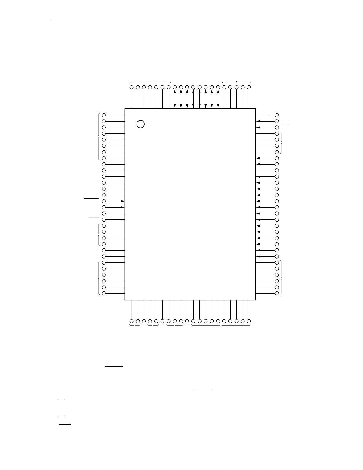
CHAPTER 1 OUTLINE (µPD78078 SUBSERIES)
100-pin plastic QFP (14 x 20 mm)
µ
PD78P078GF-3BA
100-pin ceramic WQFN
µ
PD78P078KL-T
(L)
D7D6D5D4D3D2D1
D0
(L)
(L)
V
Open
(L)
V
Open
(L)
RESET
A9
(L)
PGM
(L)
V
DD
23
SS
24
V
(L)
8889919293949698100 87909799 8195 85
1
86
2
3
4
5
6
7
8
PP
9
10
11
DD
12
13
14
15
16
17
18
19
20
21
22
23
24
25
26
27
28
29
30
434240393837353331 44413432
45
828384
80
79
78
(L)
CE
OE
77
76
75
(L)
74
73
72
71
70
69
68
67
66
65
64
63
62
61
60
59
58
57
A15
A14
V
SS
A13
A12
A11
A10
A16
A8
A7
A6
A5
A4
A3
A2
A1
A0
56
55
54
53
(L)
52
51
494847
5036 46
(L)
SS
V
(L)
DD
V
(L)
SS
V
(L)
Cautions 1. (L) : Connect independently to VSS via a pull-down resistor.
2. VSS : Connect to the ground.
3. RESET : Set to the low level.
4. Open : Leave open.
A0 to A16 : Address Bus RESET : Reset
CE : Chip Enable V
DD : Power Supply
D0 to D7 : Data Bus VPP : Programming Power Supply
OE : Output Enable VSS : Ground
PGM : Program
41

CHAPTER 1 OUTLINE (µPD78078 SUBSERIES)
1.6 78K/0 Series Expansion
The products in the 78K/0 Series are listed below. The names in boxes are subseries names.
Mass-produced products
Products under development
The subseries whose name ends with Y support
2
C bus specifications.
the I
Control
100-pin
100-pin Added timers to µPD78054 and enhanced external interface
100-pin
100-pin
80-pin Enhanced serial I/O of µPD78054, reduced EMI noise version
80-pin
80-pin
64-pin
64-pin
64-pin
64-pin
64-pin
64-pin
64-pin
42-/44-pin
µPD78075B
µPD78078 µPD78078Y
µPD78070A µPD78070AY
µ
PD780018AY
µPD780058
µPD78058F
µPD78054
µPD780034
µPD780024
µPD780058Y
µPD78058FY
µPD78054Y
µPD780034Y
µPD780024Y
µPD78014H
µPD78018F
µPD78014
µPD78018FY
µPD78014Y
µPD780001
µPD78002
µPD78002Y
µPD78083
Reduced EMI noise version of µPD78078
ROM-less version of µPD78078
Enhanced serial I/O of µPD78078Y and functions are defined.
Note
Reduced EMI noise version of µPD78054
Added UART and D/A to µPD78014 and enhanced I/Os
Enhanced A/D of µPD780024
Enhanced serial I/O of µPD78018F
Reduced EMI noise version of µPD78018F
Low-voltage (1.8 V) version of µPD78014 and enhanced ROM/RAM size options
Added A/D and 16-bit timer to µPD78002
Added A/D to µPD78002
Basic subseries for control applications
Equipped with UART and operates at low-voltage (1.8 V)
78K/0
Series
64-pin
64-pin
100-pin
100-pin
80-pin
100-pin
100-pin
100-pin
80-pin
Inverter control
µPD78098864-pin
µPD780964
µPD780924
Enhanced inverter control, timer, and SIO of µPD780964, expanded ROM and RAM
Enhanced A/D of µPD780924
Equipped with inverter control circuit and UART, reduced EMI noise version
FIPTM driving
µPD780208
µPD780228
µPD78044H
Enhanced I/O and FIP C/D of µPD78044F, 53 display outputs
Enhanced I/O and FIP C/D of µPD78044H, 48 display outputs
Added N-ch open-drain I/O to µPD78044F, 34 display outputs
µPD78044F80-pin Basic subseries for driving FIPs, 34 display outputs
LCD driving
µPD780308
µPD78064B
µPD78064
TM
supported
IEBus
µPD78098B
µPD780308Y
µPD78064Y
Enhanced SIO of µPD78064, expanded ROM and RAM
Reduced EMI noise version of µPD78064
Basic subseries for driving LCDs, equipped with UART
Reduced EMI noise version of µPD78098
µPD7809880-pin Added IEBus controller to µPD78054
Meter control
µPD78097380-pin
Equipped with controller/driver for driving automobile meters
Note Planned
42

CHAPTER 1 OUTLINE (µPD78078 SUBSERIES)
The following shows the major differences between subseries products.
Function ROM Timer 8-bit 10-bit 8-bit Serial Interface I/O VDD
Subseries Name
ControlµPD78075B 32 K to 40 K 4 ch 1 ch 1 ch 1 ch 8 ch – 2 ch 3 ch (UART: 1 ch) 88 1.8 V √
µ
PD78078 48 K to 60 K
µ
PD78070A – 61 2.7 V
µ
PD780058 24 K to 60 K 2 ch
µ
PD78058F 48 K to 60 K 3 ch (UART: 1 ch) 69 2.7 V
µ
PD78054 16 K to 60 K 2.0 V
µ
PD780034 8 K to 32 K – 8 ch –
µ
PD780024 8 ch –
µ
PD78014H 2 ch 53
µ
PD78018F 8 K to 60 K
µ
PD78014 8 K to 32 K 2.7 V
µ
PD780001 8 K – – 1 ch 39 –
µ
PD78002 8 K to 16 K 1 ch – 53 √
µ
PD78083 – 8 ch
InverterµPD780988 32 K to 60 K 3 ch
control
FIP
driving
LCD
driving UART: 1 ch)
µ
PD780964 8 K to 32 K
µ
PD780924 8 ch
µ
PD780208 32 K to 60 K 2 ch 1 ch 1 ch 1 ch 8 ch – – 2 ch 74 2.7 V –
µ
PD780228 48 K to 60 K 3 ch – – 1 ch 72 4.5 V
µ
PD78044H 32 K to 48 K 2 ch 1 ch 1 ch 68 2.7 V
µ
PD78044F 16 K to 40 K 2 ch
µ
PD780308 48 K to 60 K 2 ch 1 ch 1 ch 1 ch 8 ch – –
µ
PD78064B 32 K 2 ch (UART: 1 ch)
Capacity 8-bit 16-bit
Note 1
Note 2
Watch
WDT A/D A/D D/A
– 1 ch – 8 ch
MIN. Value Expansion
3 ch (Time division
UART: 1 ch)
3 ch (UART: 1 ch, Time
division 3-wire: 1 ch)
1 ch (UART: 1 ch)
–
3 ch (UART: 2 ch) 47 4.0 V √
2 ch (UART: 2 ch) 2.7 V
–
3 ch (Time division
68 1.8 V
51 1.8 V
33 1.8 V –
57 2.0 V –
Externa
l
µ
PD78064 16 K to 32 K
IEBusµPD78098B 40 K to 60 K 2 ch 1 ch 1 ch 1 ch 8 ch – 2 ch 3 ch (UART: 1 ch) 69 2.7 V √
supported
MeterµPD780973 24 K to 32 K 3 ch 1 ch 1 ch 1 ch 5 ch – – 2 ch (UART: 1 ch) 56 4.5 V –
control
µ
PD78098 32 K to 60 K
Notes 1. 16-bit timer: 2 channels
10-bit timer: 1 channel
2. 10-bit timer: 1 channel
43

1.7 Block Diagram
CHAPTER 1 OUTLINE (µPD78078 SUBSERIES)
TO0/P30
TI00/INTP0/P00
TI01/INTP1/P01
TO1/P31
TI1/P33
TO2/P32
TI2/P34
TI5/TO5/P100
TI6/TO6/P101
SI0/SB0/P25
SO0/SB1/P26
SCK0/P27
SI1/P20
SO1/P21
SCK1/P22
STB/P23
BUSY/P24
SI2/RxD/P70
SO2/TxD/P71
SCK2/ASCK/P72
ANI0/P10 to
ANI7/P17
AV
AV
AV
REF0
ANO0/P130,
ANO1/P131
AV
AV
REF1
INTP0/P00 to
INTP6/P06
BUZ/P36
PCL/P35
16-bit TIMER/
Event Counter
Port 0
Port 1
P01 to P06
P07
P10 to P17
8-bit TIMER/
P00
Event Counter 1
Port 2
P20 to P27
8-bit TIMER/
Event Counter 2
Port 3
P30 to P37
8-bit TIMER/
Event Counter 5
8-bit TIMER/
Event Counter 6
Watchdog Timer
Watch Timer
Serial
78K/0
CPU Core
ROM
Port 4
Port 5
Port 6
Port 7
Port 8
P40 to P47
P50 to P57
P60 to P67
P70 to P72
P80 to P87
Interface 0
Port 9
Serial
Interface 1
RAM
Serial
Interface 2
Port 10
Port 12
Port 13
Real-Time
Output Port
DD
SS
A/D Converter
P90 to P96
P100 to P103
P120 to P127
P130, P131
RTP0/P120 to
RTP7/P127
AD0/P40 to
AD7/P47
A0/P80 to
A7/P87
External
SS
D/A Converter
Access
A8/P50 to
A15/P57
RD/P64
WR/P65
Interrupt
Control
Buzzer Output
Clock Output
Control
VDDV
System
SS
IC
(V
PP
)
Control
WAIT/P66
ASTB/P67
RESET
X1
X2
XT1/P07
XT2
44
Remarks 1. The internal ROM and RAM capacities depend on the product.
µ
2. Pin connection in parentheses is for the
PD78P078.

1.8 Outline of Function
CHAPTER 1 OUTLINE (µPD78078 SUBSERIES)
Part Number
µ
PD78076
µ
PD78078
µ
PD78P078
Item
Internal ROM Mask ROM PROM
memory 48 Kbytes 60 Kbytes 60 Kbytes
High-speed RAM 1024 bytes
Buffer RAM 32 bytes
Expansion RAM 1024 bytes 1024 bytes
Memory space 64 Kbytes
General register 8 bits x 8 x 4 banks
Minimum
instruction
execution
time
With main system clock selected 0.4 µs/0.8 µs/1.6 µs/3.2 µs/6.4 µs/12.8 µs (@ 5.0-MHz operation)
With subsystem clock selected 122 µs (@ 32.768-kHz operation)
Instruction set • 16-bit operation
• Multiply/divide (8-bit x 8-bit, 16-bit/8-bit)
• Bit manipulate (set, reset, test, and Boolean operation)
• BCD adjust, etc.
I/O port Total : 88
• CMOS input : 2
• CMOS input/output : 78
• N-ch open drain I/O : 8
A/D converter 8-bit resolution x 8 channels
Note 1
Note 2
D/A converter 8-bit resolution x 2 channels
Serial interface •
3-wire serial I/O/SBI/2-wire serial I/O mode selection possible
: 1 channel
• 3-wire serial I/O mode (Maximum 32-byte on-chip
automatic transmit/receive function) : 1 channel
• 3-wire serial I/O/UART mode selection possible : 1 channel
Timer • 16-bit timer/event counter : 1 channel
• 8-bit timer/event counter : 4 channels
• Watch timer : 1 channel
• Watchdog timer : 1 channel
Timer output 5 outputs: (14-bit PWM output enable: 1, 8-bit PWM output enable: 2)
Clock output 19.5 kHz, 39.1 kHz, 78.1 kHz, 156 kHz, 313 kHz, 625 kHz, 1.25 MHz,
2.5 MHz, 5.0 MHz (@ 5.0-MHz operation with main system clock)
32.768 kHz (@ 32.768-kHz operation with subsystem clock)
Buzzer output
1.2 kHz, 2.4 kHz, 4.9 kHz, 9.8 kHz (@ 5.0-MHz operation with main system clock)
Notes 1. The capacity of the internal PROM can be changed using the internal memory size switching register
(IMS).
2. The capacity of the internal expansion RAM can be changed using the internal expansion RAM size
switching register (IXS).
45

CHAPTER 1 OUTLINE (µPD78078 SUBSERIES)
Part Number
Item
Vectored Maskable Internal: 15
interrupt External: 7
source Non-maskable Internal: 1
Software Internal: 1
Test input Internal: 1
Power supply voltage VDD = 1.8 to 5.5 V
Operating ambient temperature T A = –40 to +85°C
Package • 100-pin plastic QFP (Fine pitch) (14 x 14 mm, resin thickness 1.45 mm)
µ
PD78076
External: 1
•
100-pin plastic LQFP
• 100-pin plastic QFP (14 x 20 mm, resin thickness 2.7 mm)
• 100-pin ceramic WQFN (14 x 20 mm) (µPD78P078 only)
Note
µ
PD78078
(Fine pitch) (14 x 14 mm, resin thickness 1.4 mm)
µ
PD78P078
Note Under development
46

CHAPTER 1 OUTLINE (µPD78078 SUBSERIES)
1.9 Mask Options
The mask ROM versions (µPD78076, 78078) provide pull-up register mask options which allow users to specify
whether to connect a pull-up register to a specific port pin when the user places an order for the device production.
Using this mask option when pull-up resistors are required reduces the number of components to add to the device,
resulting in board space saving.
µ
The mask options provided in the
PD78078 Subseries are shown in Table 1-1.
Table 1-1. Mask Options of Mask ROM Versions
Pin Names Mask Options
P60 to P63, P90 to P93 Pull-up resistor connection can be specified
in 1-bit units.
1.10 Differences with µPD78054 Subseries
The µPD78078 Subseries is upward-compatible with the µPD78054 Subseries. The differences between the two
subseries are shown in the table below. The functions and specifications other than those shown in this table are
common to these two series.
µ
Table 1-2. Differences between
Subseries
Item
No. of I/O ports 69 88
8-bit timer/event counter 2 channnels 4 channels
External device Address bus separate function Address bus separate function
expansion function is not provided. is provided. (P80/A0 to P87/A7)
Power supply voltage VDD = 2.0 to 6.0 V VDD = 1.8 to 5.5 V
Package 80-pin plastic TQFP (12 x 12 mm) 100-pin plastic TQFP (14 x 14 mm)
80-pin plastic QFP (14 x 14 mm) 100-pin plastic LQFP (14 x 14 mm)
80-pin plastic WQFP (14 x 14 mm)* 100-pin plastic QFP (14 x 20 mm)
* : Only for PROM version * : Only for PROM version
PD78078 Subseries and µPD78054 Subseries
µ
PD78054 Subseries
100-pin plastic WQFP (14 x 20 mm)*
µ
PD78078 Subseries
47

[MEMO]
48

CHAPTER 2 OUTLINE (µPD78078Y SUBSERIES)
2.1 Features
Internal high-capacity ROM and RAM
Type
Part Number
µ
PD78076Y
µ
PD78078Y
µ
PD78P078Y
Program Memory
(ROM)
48 Kbytes
60 Kbytes
60 Kbytes
Note 1
Internal High-Speed RAM
1024 bytes 32 bytes
Data Memory
Internal Buffer RAM
Internal Expansion RAM
1024 bytes
1024 bytes
Note 2
Notes 1. The capacity of internal PROM can be changed using the internal memory size switching register
(IMS).
2. The capacity of internal high-speed RAM can be changed using the internal expansion RAM size
switching register (IXS).
External memory expansion space: 64 Kbytes
Minimum instruction execution time changeable from high speed (0.4 µs: @ 5.0-MHz operation with main
µ
system clock) to ultra-low speed (122
s: @ 32.768-kHz operation with subsystem clock)
Instruction set suited to system control
• Bit manipulation possible in all address spaces
• Multiply and divide instructions incorporated
88 I/O port pins: (including eight N-ch open-drain port pins)
8-bit resolution A/D converter: 8 channels
8-bit resolution D/A converter: 2 channels
Serial interface: Three channels
2
• 3-wire serial I/O/2-wire serial I/O/I
C bus mode: 1 channel
• 3-wire serial I/O mode (Automatic transmit/receive function): 1 channel
• 3-wire serial I/O/UART mode: 1 channel
Timer: Seven channels
• 16-bit timer/event counter : 1 channel
• 8-bit timer/event counter : 4 channels
• Watch timer : 1 channel
• Watchdog timer : 1 channel
24 vectored interrupt sources
Two test inputs
Two types of on-chip clock oscillation circuits (main system clock and subsystem clock)
Power supply voltage: 1.8 to 5.5 V
49

CHAPTER 2 OUTLINE (µPD78078Y SUBSERIES)
2.2 Application Fields
Cellular phones, cordless telephones, printers, AV equipment, air conditioners, cameras, PPCs, fuzzy home
appliances, vending machines, etc.
2.3 Ordering Information
Part number Package Internal ROM
µ
PD78076YGC-xxx-8EU
µ
PD78076YGF-xxx-3BA 100-pin plastic QFP (14 x 20 mm, resin thickness 2.7 mm) Mask ROM
µ
PD78078YGC-xxx-8EU
µ
PD78078YGF-xxx-3BA 100-pin plastic QFP (14 x 20 mm, resin thickness 2.7 mm) Mask ROM
µ
PD78P078YGC-8EU
µ
PD78P078YGF-3BA 100-pin plastic QFP (14 x 20 mm, resin thickness 2.7 mm) One-time PROM
µ
PD78P078YKL-T 100-pin ceramic WQFN (14 x 20 mm) EPROM
Note
100-pin plastic LQFP (Fine pitch) (14 x 14 mm, resin thickness 1.4 mm) Mask ROM
Note
100-pin plastic LQFP (Fine pitch) (14 x 14 mm, resin thickness 1.4 mm) Mask ROM
Note
100-pin plastic LQFP (Fine pitch) (14 x 14 mm, resin thickness 1.4 mm) One-time PROM
Note Under development
Remark xxx indicates ROM code suffix.
50

CHAPTER 2 OUTLINE (µPD78078Y SUBSERIES)
2.4 Quality Grade
Part number Package Quality grades
µ
PD78076YGC-xxx-8EU
µ
PD78076YGF-xxx-3BA 100-pin plastic QFP (14 x 20 mm, resin thickness 2.7 mm) Standard
µ
PD78078YGC-xxx-8EU
µ
PD78078YGF-xxx-3BA 100-pin plastic QFP (14 x 20 mm, resin thickness 2.7 mm) Standard
µ
PD78P078YGC-8EU
µ
PD78P078YGF-3BA 100-pin plastic QFP (14 x 20 mm, resin thickness 2.7 mm) Standard
µ
PD78P078YKL-T 100-pin ceramic WQFN (14 x 20 mm)
Note Under development
Caution Of the above members, the following device with the suffix KL-T should be used only for
experiment or function evaluation, because it is not intended for use in equipment that will be
mass-produced and require high reliability.
Note
100-pin plastic LQFP (Fine pitch) (14 x 14 mm, resin thickness 1.4 mm) Standard
Note
100-pin plastic LQFP (Fine pitch) (14 x 14 mm, resin thickness 1.4 mm) Standard
Note
100-pin plastic LQFP (Fine pitch) (14 x 14 mm, resin thickness 1.4 mm) Standard
µ
PD78P078YKL-T
•
Not assured
(for function evaluation only)
Remark xxx indicates ROM code suffix.
Please refer to “Quality Grades on NEC Semiconductor Devices”(C11531E) published by NEC Corporation to know the
specification of quality grade on the devices and its recommended applications.
51

CHAPTER 2 OUTLINE (µPD78078Y SUBSERIES)
2.5 Pin Configuration (Top View)
(1) Normal operating mode
100-pin plastic LQFP (Fine pitch) (14 x 14 mm, resin thickness 1.4 mm)
µ
PD78076YGC-xxx-8EU
µ
PD78P078YGC-8EU
Note Under development
Note
, 78078YGC-xxx-8EU
Note
Note
52

P14/ANI4
P15/ANI5
P16/ANI6
P17/ANI7
AV
P130/ANO0
P131/ANO1
AV
REF1
P70/SI2/RxD
P71/SO2/TxD
P72/SCK2/ASCK
V
P20/SI1
P21/SO1
P22/SCK1
P23/STB
P24/BUSY
P25/SI0/SB0/SDA0
P26/SO0/SB1/SDA1
P27/SCK0/SCL
P80/A0
P81/A1
P82/A2
P83/A3
P84/A4
CHAPTER 2 OUTLINE (µPD78078Y SUBSERIES)
)
REF0AVDD
P13/ANI3
P12/ANI2
P11/ANI1
P10/ANI0
AV
P06/INTP6
P05/INTP5
P04/INTP4
P03/INTP3
P02/INTP2
P01/INTP1/TI01
P00/INTP0/TI00
RESET
XT1/P07
XT2
100
9998 97 9695 94 93 92 90 8988 87 868584 83 82 81 8079 7877 7691
1
2
3
4
SS
5
6
7
8
9
10
11
SS
12
13
14
15
16
17
18
19
20
21
22
23
24
25
262728 293031 3233 34 36 3738394041 42 43 444546474849 5035
PP
VDDX1X2IC (V
P127/RTP7
P126/RTP6
P125/RTP5
P124/RTP4
P123/RTP3
75
74
73
72
71
70
69
68
67
66
65
64
63
62
61
60
59
58
57
56
55
54
53
52
51
P122/RTP2
P121/RTP1
P120/RTP0
P96
P95
P94
P93
P92
P91
P90
P37
P36/BUZ
P35/PCL
P34/TI2
P33/TI1
P32/TO2
P31/TO1
P30/TO0
P103
P102
P101/TI6/TO6
P100/TI5/TO5
P67/ASTB
P66/WAIT
P65/WR
SS
V
P85/A5
P86/A6
P87/A7
P40/AD0
P41/AD1
P42/AD2
P43/AD3
P44/AD4
P45/AD5
P46/AD6
P47/AD7
P50/A8
P51/A9
P52/A10
P53/A11
P54/A12
P56/A14
P55/A13
P57/A15
Cautions 1. Connect IC (Internally Connected) pin to VSS directly.
2. Connect AV
DD pin to VDD.
3. Connect AVSS pin to VSS.
µ
Remark Pin connection in parentheses is for the
PD78P078Y.
P60
P61
P62
P63
P64/RD
53

CHAPTER 2 OUTLINE (µPD78078Y SUBSERIES)
100-pin plastic QFP (14 x 20 mm)
µ
PD78076YGF-xxx-3BA
µ
PD78078YGF-xxx-3BA, 78P078YGF-3BA
100-pin ceramic WQFN (14 x 20 mm)
µ
PD78P078YKL-T
P96
P95
P94
P93
P92
P91
P90
P37
P36/BUZ
P35/PCL
P34/TI2
P33/TI1
P32/TO2
P31/TO1
P30/TO0
P103
P102
P101/TI6/TO6
P100/TI5/TO5
P67/ASTB
P120/RTP0
P121/RTP1
P122/RTP2
P123/RTP3
P124/RTP4
P125/RTP5
P126/RTP6
P127/RTP7
IC (V
PP
X2
X1
V
XT2
XT1/P07
RESET
P00/INTP0/TI00
P01/INTP1/TI01
P02/INTP2
P03/INTP3
P04/INTP4
P05/INTP5
P06/INTP6
AV
AV
REF0
P10/ANI0
P11/ANI1
P12/ANI2
P13/ANI3
P14/ANI4
P15/ANI5
8889919293949698100 87909799 8195 85
1
86
2
3
4
5
6
7
8
)
9
10
11
DD
12
13
14
15
16
17
18
19
20
21
22
DD
23
24
25
26
27
28
29
30
434240393837353331 44413432
45
828384
80
79
78
77
76
75
74
73
72
71
70
69
68
67
66
65
64
63
62
61
60
59
58
57
56
55
54
53
52
51
494847
5036 46
P66/WAIT
P65/WR
P64/RD
P63
P62
P61
P60
P57/A15
P56/A14
V
SS
P55/A13
P54/A12
P53/A11
P52/A10
P51/A9
P50/A8
P47/AD7
P46/AD6
P45/AD5
P44/AD4
P43/AD3
P42/AD2
P41/AD1
P40/AD0
P87/A7
P86/A6
P85/A5
P84/A4
P83/A3
P82/A2
54
SS
AV
P16/ANI6
P17/ANI7
REF1
AV
P130/ANO0
P131/ANO1
P70/SI2/RxD
SS
V
P20/SI1
P71/SO2/TxD
P72/SCK2/ASCK
Cautions 1. Connect IC (Internally Connected) pin to V
2. Connect AVDD pin to VDD.
3. Connect AVSS pin to VSS.
Remark Pin connection in parentheses is for the
µ
PD78P078Y.
P23/STB
P21/SO1
P22/SCK1
P24/BUSY
SS directly.
P80/A0
P81/A1
P27/SCK0/SCL
P25/SI0/SB0/SDA0
P26/SO0/SB1/SDA1

Pin Identifications
CHAPTER 2 OUTLINE (µPD78078Y SUBSERIES)
A0 to A15 : Address Bus
AD0 to AD7 : Address/Data Bus
ANI0 to ANI7 : Analog Input
ANO0, ANO1 : Analog Output
ASCK : Asynchronous Serial Clock
ASTB : Address Strobe
DD : Analog Power Supply
AV
AVREF0, AVREF1 : Analog Reference Voltage
AVSS : Analog Ground
BUSY : Busy
BUZ : Buzzer Clock
IC : Internally Connected
INTP0 to INTP6 : Interrupt from Peripherals
P00 to P07 : Port 0
P10 to P17 : Port 1
P20 to P27 : Port 2
P30 to P37 : Port 3
P40 to P47 : Port 4
P50 to P57 : Port 5
P60 to P67 : Port 6
P70 to P72 : Port 7
P80 to P87 : Port 8
P90 to P96 : Port 9
P100 to P103 : Port 10
P120 to P127 : Port 12
P130, P131 : Port 13
PCL : Programmable Clock
RD : Read Strobe
RESET : Reset
RTP0 to RTP7 : Real-time Output Port
RxD : Receive Data
SB0, SB1 : Serial Bus
SCK0 to SCK2 : Serial Clock
SCL : Serial Clock
SDA0, SDA1 : Serial Data
SI0 to SI2 : Serial Input
SO0 to SO2 : Serial Output
STB : Strobe
TI00, TI01 : Timer Input
TI1, TI2, TI5, TI6 : Timer Input
TO0 to TO2, TO5, TO6
: Timer Output
TxD : Transmit Data
DD : Power Supply
V
VPP : Programming Power Supply
SS : Ground
V
WAIT : Wait
WR : Write Strobe
X1, X2 : Crystal (Main System Clock)
XT1, XT2 : Crystal (Subsystem Clock)
55

CHAPTER 2 OUTLINE (µPD78078Y SUBSERIES)
(2) PROM programming mode
100-pin plastic QFP (Fine pitch) (14 x 14 mm, resin thickness 1.45 mm)
µ
PD78P078YGC-7EA
100-pin plastic LQFP (Fine pitch) (14 x 14 mm, resin thickness 1.4 mm)
µ
PD78P078YGC-8EU
Note
(L)
(L)
(L)
(L)
VSSV
DD
(L)
(L)A9RESET
PGM
888991929394959698100 8187909799
(L)
1
2
3
4
V
SS
5
6
7
V
DD
8
9
10
11
V
SS
12
13
14
15
16
17
18
19
20
21
22
23
24
25
38373534333231302826 4539362927
40
86
(L)
DD
Open
V
(L)
PP
Open
V
(L)
76
7778798082838485
75
74
73
72
71
70
(L)
69
68
67
66
65
64
63
62
61
60
59
58
D7
D6
D5
D4
D3
D2
D1
D0
57
56
55
54
(L)
53
52
51
504948474644434241
CE
56
A7
(L)
A2A3A4A5A6
A0
A1
A8
A16
A10
Note Under development
Cautions 1. (L) : Connect independently to V
2. VSS : Connect to the ground.
3. RESET : Set to the low level.
4. Open : Leave open.
SS
A11
V
A12
A13
A14
SS via a pull-down resistor.
A15
(L)
OE

CHAPTER 2 OUTLINE (µPD78078Y SUBSERIES)
100-pin plastic QFP (14 x 20 mm)
µ
PD78P078YGF-3BA
100-pin ceramic WQFN
µ
PD78P078YKL-T
(L)
V
Open
(L)
V
Open
(L)
RESET
A9
(L)
PGM
(L)
V
V
(L)
(L)
1
D7D6D5D4D3D2D1
8889919293949698100 87909799 8195 85
D0
86
2
3
4
5
6
7
8
PP
9
10
11
DD
12
13
14
15
16
17
18
19
20
21
22
DD
SS
23
24
25
26
27
28
29
30
434240393837353331 44413432
45
(L)
828384
80
79
78
(L)
CE
OE
77
76
75
(L)
74
73
72
71
70
69
68
67
66
65
64
63
62
61
60
59
58
57
A15
A14
V
SS
A13
A12
A11
A10
A16
A8
A7
A6
A5
A4
A3
A2
A1
A0
56
55
54
53
(L)
52
51
494847
5036 46
(L)
SS
V
(L)
DD
V
(L)
SS
V
(L)
Cautions 1. (L) : Connect independently to VSS via a pull-down resistor.
2. VSS : Connect to the ground.
3. RESET : Set to the low level.
4. Open : Leave open.
A0 to A16 : Address Bus RESET : Reset
CE : Chip Enable V
DD : Power Supply
D0 to D7 : Data Bus VPP : Programming Power Supply
OE : Output Enable VSS : Ground
PGM : Program
57

CHAPTER 2 OUTLINE (µPD78078Y SUBSERIES)
2.6 78K/0 Series Expansion
The products in the 78K/0 Series are listed below. The names in boxes are subseries names.
Mass-produced products
Products under development
The subseries whose name ends with Y support
2
C bus specifications.
the I
Control
100-pin
100-pin Added timers to µPD78054 and enhanced external interface
100-pin
100-pin
80-pin Enhanced serial I/O of µPD78054, reduced EMI noise version
80-pin
80-pin
64-pin
64-pin
64-pin
64-pin
64-pin
64-pin
64-pin
42-/44-pin
µPD78075B
µPD78078 µPD78078Y
µPD78070A µPD78070AY
µ
PD780018AY
µPD780058
µPD78058F
µPD78054
µPD780034
µPD780024
µPD78014H
µPD78018F
µPD78014
µPD780001
µPD78002
µPD78083
µPD780058Y
µPD78058FY
µPD78054Y
µPD780034Y
µPD780024Y
µPD78018FY
µPD78014Y
µPD78002Y
Reduced EMI noise version of µPD78078
ROM-less version of µPD78078
Enhanced serial I/O of µPD78078Y and functions are defined.
Note
Reduced EMI noise version of µPD78054
Added UART and D/A to µPD78014 and enhanced I/Os
Enhanced A/D of µPD780024
Enhanced serial I/O of µPD78018F
Reduced EMI noise version of µPD78018F
Low-voltage (1.8 V) version of µPD78014 and enhanced ROM/RAM size options
Added A/D and 16-bit timer to µPD78002
Added A/D to µPD78002
Basic subseries for control applications
Equipped with UART and operates at low-voltage (1.8 V)
78K/0
Series
64-pin
64-pin
100-pin
100-pin
80-pin
100-pin
100-pin
100-pin
80-pin
Inverter control
µPD78098864-pin
µPD780964
µPD780924
FIP driving
µPD780208
µPD780228
µPD78044H
µPD78044F80-pin Basic subseries for driving FIPs, 34 display outputs
LCD driving
µPD780308
µPD78064B
µPD78064
IEBus supported
µPD78098B
µPD7809880-pin Added IEBus controller to µPD78054
Meter control
µPD78097380-pin
µPD780308Y
µPD78064Y
Enhanced inverter control, timer, and SIO of µPD780964, expanded ROM and RAM
Enhanced A/D of µPD780924
Equipped with inverter control circuit and UART, reduced EMI noise version
Enhanced I/O and FIP C/D of µPD78044F, 53 display outputs
Enhanced I/O and FIP C/D of µPD78044H, 48 display outputs
Added N-ch open-drain I/O to µPD78044F, 34 display outputs
Enhanced SIO of µPD78064, expanded ROM and RAM
Reduced EMI noise version of µPD78064
Basic subseries for driving LCDs, equipped with UART
Reduced EMI noise version of µPD78098
Equipped with controller/driver for driving automobile meters
Note Planned
58

CHAPTER 2 OUTLINE (µPD78078Y SUBSERIES)
Major differences among Y subseries are tabulated below.
Function ROM Configuration of Serial Interface
Subseries Capacity MIN.
Control
µ
PD78078Y 48K to 60K 3-wire/2-wire/I2C : 1 ch 88 1.8 V
µ
PD78070AY —
µ
PD780018AY
µ
PD780058Y 24K to 60K 3-wire/2-wire/I2C : 1 ch 68 1.8 V
µ
PD78058FY 48K to 60K 3-wire/2-wire/I2C : 1 ch 69 2.7 V
µ
PD78054Y 16K to 60K 3-wire with automatic transmit/receive function : 1 ch 2.0 V
µ
PD780034Y 8K to 32K UART : 1 ch 51 1.8 V
µ
PD780024Y
µ
PD78018FY 8K to 60K 3-wire/2-wire/I2C : 1 ch 53
µ
PD78014Y 8K to 32K 3-wire/2-wire/I2C : 1 ch 2.7 V
48K to 60K 3-wire with automatic transmit/receive function : 1 ch 88
3-wire with automatic transmit/receive function : 1 ch
3-wire/UART : 1 ch
Time division 3-wire : 1 ch
I2C bus (supports multi-master) : 1 ch
3-wire with automatic transmit/receive function : 1 ch
3-wire/time division UART : 1 ch
3-wire/UART : 1 ch
3-wire : 1 ch
I2C bus (supports multi-master) : 1 ch
3-wire with automatic transmit/receive function : 1 ch
3-wire with automatic transmit/receive function : 1 ch
I
/O VDD
61
2.7 V
µ
PD78002Y 8K to 16K 3-wire/2-wire/SBI/I2C : 1 ch
LCD
drive 3-wire/time division UART : 1 ch
µ
PD780308Y 48K to 60K 3-wire/2-wire/I2C : 1 ch 57 2.0 V
3-wire : 1 ch
µ
PD78064Y 16K to 32K 3-wire/2-wire/I2C : 1 ch
3-wire/UART : 1 ch
Remark The functions except serial interface are common with subseries without Y.
59

2.7 Block Diagram
CHAPTER 2 OUTLINE (µPD78078Y SUBSERIES)
TO0/P30
TI00/INTP0/P00
TI01/INTP1/P01
TO1/P31
TI1/P33
TO2/P32
TI2/P34
P100/TI5/TO5
P101/TI6/TO6
SI0/SB0/SDA0/P25
SO0/SB1/SDA1/P26
SCK0/SCL/P27
SI1/P20
SO1/P21
SCK1/P22
STB/P23
BUSY/P24
SI2/RxD/P70
SO2/TxD/P71
SCK2/ASCK/P72
ANI0/P10 to
ANI7/P17
AV
AVSS
AVREF0
ANO0/P130,
ANO1/P131
AVSS
AVREF1
INTP0/P00 to
INTP6/P06
BUZ/P36
PCL/P35
DD
16-bit TIMER/
Event Counter
8-bit TIMER/
Event Counter 1
8-bit TIMER/
Event Counter 2
8-bit TIMER/
Event Counter 5
8-bit TIMER/
Event Counter 6
Watchdog Timer
Watch Timer
Serial
Interface 0
Serial
Interface 1
Serial
Interface 2
A/D Converter
D/A Converter
Interrupt
Control
Buzzer Output
Clock Output
Control
78K/0
CPU Core
RAM
VDD VSS IC
ROM
(V
PP)
Port 0
Port 1
Port 2
Port 3
Port 4
Port 5
Port 6
Port 7
Port 8
Port 9
Port 10
Port 12
Port 13
Real-Time
Output Port
External
Access
System
Control
P00
P01 to P06
P07
P10 to P17
P20 to P27
P30 to P37
P40 to P47
P50 to P57
P60 to P67
P70 to P72
P80 to P87
P90 to P96
P100 to P103
P120 to P127
P130, P131
RTP0/P120 to
RTP7/P127
AD0/P40 to
AD7/P47
A0/P80 to
A7/P87
A8/P50 to
A15/P57
RD/P64
WR/P65
WAIT/P66
ASTB/P67
RESET
X1
X2
XT1/P07
XT2
60
Remarks 1. The internal ROM and RAM capacities depend on the product.
µ
2. Pin connection in parentheses is for the
PD78P078Y.

CHAPTER 2 OUTLINE (µPD78078Y SUBSERIES)
2.8 Outline of Function
µ
Part Number
Item
ROM
Internal
memory
Memory space 64 Kbytes
General register 8 bits x 8 x 4 banks
Minimum
instruction
execution
time
Instruction set • 16-bit operation
I/O port Total : 88
High-speed RAM 1024 bytes
Buffer RAM 32 bytes
Expansion RAM 1024 bytes 1024 bytes
With main system clock selected 0.4 µs/0.8 µs/1.6 µs/3.2 µs/6.4 µs/12.8 µs (@ 5.0-MHz operation)
With subsystem clock selected 122 µs (@ 32.768-kHz operation)
PD78076Y
Mask ROM PROM
48 Kbytes 60 Kbytes 60 Kbytes
• Multiply/divide (8-bit x 8-bit, 16-bit/8-bit)
• Bit manipulate (set, reset, test, and Boolean operation)
• BCD adjust, etc.
• CMOS input : 2
• CMOS input/output : 78
µ
PD78078Y
µ
PD78P078Y
Note 1
• N-ch open drain I/O : 8
A/D converter 8-bit resolution x 8 channels
D/A converter 8-bit resolution x 2 channels
Serial interface • 3-wire serial I/O/2-wire serial I/O/I2C bus mode selection : 1 channel
possible
• 3-wire serial I/O mode (maximum 32-byte on-chip automatic
transmit/receive function) : 1 channel
• 3-wire serial I/O/UART mode selection possible : 1 channel
Timer • 16-bit timer/event counter : 1 channel
• 8-bit timer/event counter : 4 channels
• Watch timer : 1 channel
• Watchdog timer : 1 channel
Timer output 5 outputs: (14-bit PWM output enable: 1, 8-bit PWM output enable: 2)
Clock output 19.5 kHz, 39.1 kHz, 78.1 kHz, 156 kHz, 313 kHz, 625 kHz, 1.25 MHz,
2.5 MHz, 5.0 MHz (@ 5.0-MHz operation with main system clock)
32.768 kHz (@ 32.768-kHz operation with subsystem clock)
Buzzer output 1.2 kHz, 2.4 kHz, 4.9 kHz, 9.8 kHz
(@ 5.0-MHz operation with main system clock)
Notes 1. The capacity of the internal PROM can be changed using the internal memory size switching register
(IMS).
2. The capacity of the internal expansion RAM can be changed using the internal expansion RAM size
switching register (IXS).
61

CHAPTER 2 OUTLINE (µPD78078Y SUBSERIES)
µ
Item
Part Number
Vectored Maskable Internal: 15
interrupt External: 7
source Non-maskable Internal: 1
Software Internal: 1
Test input Internal: 1
Power supply voltage VDD = 1.8 to 5.5 V
Operating ambient temperature T A = –40 to +85°C
Package •
PD78076Y
External: 1
100-pin plastic LQFP
• 100-pin plastic QFP (14 x 20 mm, resin thickness 2.7 mm)
• 100-pin ceramic WQFN (14 x 20 mm) (µPD78P078Y only)
Note Under development
µ
PD78078Y
Note
(Fine pitch) (14 x 14 mm, resin thickness 1.4 mm)
µ
PD78P078Y
62

CHAPTER 2 OUTLINE (µPD78078Y SUBSERIES)
2.9 Mask Options
The mask ROM versions (µPD78076Y, 78078Y) provide pull-up register mask options which allow users to specify
whether to connect a pull-up register to a specific port pin when the user places an order for the device production.
Using this mask option when pull-up resistors are required reduces the number of components to add to the device,
resulting in board space saving.
µ
The mask options provided in the
PD78078Y Subseries are shown in Table 2-1.
Table 2-1. Mask Options of Mask ROM Versions
Pin Names Mask Options
P60 to P63, P90 to P93 Pull-up resistor connection can be specified
in 1-bit units.
2.10 Differences with µPD78054Y Subseries
The µPD78078Y Subseries is upward-compatible with the µPD78054Y Subseries. The differences between the
two subseries are shown in the table below. The functions and specifications other than those shown in this table
are common to these two series.
µ
Table 2-2. Differences between
Subseries
Item
No. of I/O ports 69 88
8-bit timer/event counter 2 channnels 4 channels
External device Address bus separate function Address bus separate function
expansion function is not provided. is provided. (P80/A0 to P87/A7)
Power supply voltage VDD = 2.0 to 6.0 V VDD = 1.8 to 5.5 V
Package 80-pin plastic QFP (14 x 14 mm) 100-pin plastic QFP (14 x 20 mm)
80-pin plastic WQFP (14 x 14 mm)* 100-pin plastic LQFP (14 x 14 mm)
* : Only for PROM version 100-pin plastic WQFP (14 x 20 mm)*
PD78078Y Subseries and µPD78054Y Subseries
µ
PD78054Y Subseries
* : Only for PROM version
µ
PD78078Y Subseries
63

[MEMO]
64

CHAPTER 3 PIN FUNCTION (µPD78078 SUBSERIES)
3.1 Pin Function List
3.1.1 Normal operating mode pins
(1) Port pins (1/3)
Pin Name
P00 Input Input only Input INTP0/TI00
P01 Input/output mode can be specified INTP1/TI01
P02 bit-wise. INTP2
P03 Input/ Port 0. If used as an input port, an on-chip INTP3
P04 output 8-bit input/output port. pull-up resistor can be connected INTP4
P05 by software. INTP5
P06 INTP6
P07
P10 to P17 Port 1.
P20 SI1
P21 SO1
P22 Port 2. SCK1
P23 Input/ 8-bit input/output port. STB
P24 output Input/output mode can be specified bit-wise. BUSY
P25 If used as an input port, an on-chip pull-up resistor can be connected by SI0/SB0
P26 software. SO0/SB1
P27 SCK0
Note 1
Input/Output
Input Input only Input XT1
8-bit input/output port.
Input/
output
Input/output mode can be specified bit-wise. Input ANI0 to ANI7
If used as input port, an on-chip pull-up resistor can be connected by
software
Note 2
.
Function After Reset
Input
Input
Alternate Function
Notes 1. When the P07/XT1 pin is used as an input port, set the bit 6 (FRC) of the processor clock control
register (PCC) to 1 (do not use the feedback resistor internal to the subsystem clock oscillator).
2. When pins P10/ANI0 to P17/ANI7 are used as an analog input of the A/D converter, set port 1 in
the input mode. The on-chip pull-up resistor becomes automatically disabled.
65

(1) Port pins (2/3)
CHAPTER 3 PIN FUNCTION (µPD78078 SUBSERIES)
Pin Name
P30 TO0
P31 TO1
P32 Port 3. TO2
P33 Input/ 8-bit input/output port. TI1
P34 output Input/output mode can be specified bit-wise. TI2
P35 If used as an input port, an on-chip pull-up resistor can be connected by PCL
P36 software. BUZ
P37 —
P40 to P47 Input AD0 to AD7
P50 to P57
P61
P62 Port 6. —
P63 Input/ 8-bit input/output port.
P64 output Input/output mode can be If used as an input port, an on-chip Input RD
P65 specified bit-wise. pull-up resistor can be connected WR
P66 by software. WAIT
P67 ASTB
P70 SI2/RxD
P71
P72 SCK2/ASCK
P80 to P87 Input A0 to A7
Input/Output
Port 4.
8-bit input/output port.
Input/ Input/output mode can be specified in 8-bit units.
output If used as an input port, an on-chip pull-up resistor can be connected by
software.
Test input flag (KRIF) is set to 1 by falling edge detection.
Port 5.
8-bit input/output port.
Input/
output
Input/
output
Input/
output
LEDs can be driven directly.
Input/output mode can be specified bit-wise.
If used as an input port, an on-chip pull-up resistor can be connected
by software.
Port 7.
3-bit input/output port.
Input/output mode can be specified bit-wise.
If used as an input port, an on-chip pull-up resistor can be connected
by software.
Port 8.
8-bit input/output port.
Input/output mode can be specified bit-wise.
If used as an input port, an on-chip pull-up resistor can be connected
by software.
Function After Reset
N-ch open drain input/output port.
On-chip pull-up resistor can be
specified by mask option.
(Mask ROM version only).
LEDs can be driven directly.
Alternate Function
Input
Input A8 to A15
Input
SO2/TxD
66

(1) Port pins (3/3)
CHAPTER 3 PIN FUNCTION (µPD78078 SUBSERIES)
Pin Name
P90
P91 Port 9.
P92 7-bit input/output port.
P93 Input/output mode can be Input —
P94 specified bit-wise. If used as an input port, an on-chip
P95 pull-up resistor can be connected
P96 by software.
P100 TI5/TO5
P101 Input TI6/TO6
P102, P103 —
P120 to P127
P130, P131
Input/Output
Input/
output
Input/
output
Input/
output
Input/
output
Function After Reset
N-ch open-drain input/output port.
On-chip pull-up resistor can be
specified by mask option.
(Mask ROM version only).
LEDs can be driven directly.
Port 10.
4-bit input/output port.
Input/output mode can be specified bit-wise.
If used as an input port, an on-chip pull-up resistor can be connected
by software.
Port 12.
8-bit input/output port.
Input/output mode can be specified bit-wise.
If used as an input port, an on-chip pull-up resistor can be connected
by software.
Port 13.
2-bit input/output port.
Input/output mode can be specified bit-wise.
If used as an input port, an on-chip pull-up resistor can be connected
by software.
Alternate Function
Input RTP0 to RTP7
Input ANO0, ANO1
67

(2) Non-port pins (1/2)
CHAPTER 3 PIN FUNCTION (µPD78078 SUBSERIES)
Pin Name
INTP0 P00/TI00
INTP1 P01/TI01
INTP2 External interrupt request inputs with specifiable valid edges (rising edge, P02
INTP3 Input falling edge, both rising and falling edges). Input P03
INTP4 P04
INTP5 P05
INTP6 P06
SI0 P25/SB0
SI1 Input Serial interface serial data input Input P20
SI2 P70/RxD
SO0 P26/SB1
SO1 Output Serial interface serial data output Input P21
SO2 P71/TxD
SB0 Input/ P25/SI0
SB1 output P26/SO0
SCK0 P27
SCK1 Serial interface serial clock input/output Input P22
SCK2 P72/ASCK
STB Output Serial interface automatic transmit/receive strobe output Input P23
BUSY Input Serial interface automatic transmit/receive busy input Input P24
RxD Input Asynchronous serial interface serial data input Input P70/SI2
TxD Output Asynchronous serial interface serial data output Input P71/SO2
ASCK Input Asynchronous serial interface serial clock input Input P72/SCK2
TI00 External count clock input to 16-bit timer (TM0) P00/INTP0
TI01 Capture trigger signal input to capture register (CR00) P01/INTP1
TI1 External count clock input to 8-bit timer (TM1) P33
TI2 External count clock input to 8-bit timer (TM2) P34
TI5 External count clock input to 8-bit timer (TM5) P100/TO5
TI6 External count clock input to 8-bit timer (TM6) P101/TO6
TO0 16-bit timer (TM0) output (also used for 14-bit PWM output) P30
TO1 8-bit timer (TM1) output P31
TO2 Output 8-bit timer (TM2) output Input P32
TO5 8-bit timer (TM5) output (also used for 8-bit PWM output) P100/TI5
TO6 8-bit timer (TM6) output (also used for 8-bit PWM output) P101/TI6
PCL Output Clock output (for main system clock and subsystem clock trimming) Input P35
BUZ Output Buzzer output Input P36
RTP0 to RTP7
Input/Output
Serial interface serial data input/output Input
Input/
output
Input Input
Output Real-time output port outputting data in synchronization with trigger Input P120 to P127
Function After Reset
Alternate Function
68

(2) Non-port pins (2/2)
CHAPTER 3 PIN FUNCTION (µPD78078 SUBSERIES)
Pin Name
AD0 to AD7
A0 to A7 Output Low-order address bus when expanding external memory Input P80 to P87
A8 to A15 Output High-order address bus when expanding external memory Input P50 to P57
RD Strobe signal output for read operation from external memory P64
WR Strobe signal output for write operation to external memory P65
WAIT Input Wait insertion when accessing external memory Input P66
ASTB Output Input P67
ANI0 to ANI7
ANO0, ANO1
AVREF0 Input A/D converter reference voltage input — —
AVREF1 Input D/A converter reference voltage input — —
AVDD — A/D converter analog power supply. Connect to V DD.——
AVSS — A/D converter, D/A converter ground potential. Connect to VSS.——
RESET Input System reset input — —
X1 Input ——
X2 — ——
XT1 Input Input P07
XT2 — ——
VDD — Positive power supply — —
VPP — ——
VSS — Ground potential — —
Input/Output
Input/Output
Output Input
Input A/D converter analog input Input P10 to P17
Output D/A converter analog output Input P130, P131
IC — Internally connected. Connect directly to VSS. ——
Low-order address/data bus when expanding external memory Input P40 to P47
Strobe output externally latching address information output to ports 4,
5 to access external memory
Crystal connection for main system clock oscillation
Crystal connection for subsystem clock oscillation
High-voltage application for program write/verify. Connect directly to
VSS in normal operating mode.
Function After Reset
Alternate Function
3.1.2 PROM programming mode pins (µPD78P078 only)
Pin Name
RESET Input When +5 V or +12.5 V is applied to the VPP pin or a low level voltage is applied to the RESET pin,
VPP Input High-voltage application for PROM programming mode setting and program write/verify.
A0 to A16 Input Address bus
D0 to D7
OE Input Read strobe input to PROM
PGM Input Program/program inhibit input in PROM programming mode
VDD — Positive power supply
VSS — Ground potential
Input/Output
PROM programming mode setting.
the PROM programming mode is set.
Input/output
CE Input PROM enable input/program pulse input
Data bus
Function
69

CHAPTER 3 PIN FUNCTION (µPD78078 SUBSERIES)
3.2 Description of Pin Functions
3.2.1 P00 to P07 (Port 0)
These are 8-bit input/output ports. Besides serving as input/output ports, they function as an external interrupt
request input, an external count clock input to the timer, a capture trigger signal input, and crystal connection for
subsystem oscillation.
The following operating modes can be specified bit-wise.
(1) Port mode
P00 and P07 function as input-only ports and P01 to P06 function as input/output ports.
P01 to P06 can be specified for input or output ports bit-wise with a port mode register 0 (PM0). When they are
used as input ports, on-chip pull-up resistors can be connected to them by defining the pull-up resistor option
register L (PUOL).
(2) Control mode
In this mode, these ports function as an external interrupt request input, an external count clock input to
the timer, and crystal connection for subsystem clock oscillation.
(a) INTP0 to INTP6
INTP0 to INTP6 are external interrupt request input pins which can specify valid edges (rising edge,
falling edge, and both rising and falling edges). INTP0 or INTP1 becomes a 16-bit timer/event counter
capture trigger signal input pin with a valid edge input.
(b) TI00
Pin for external count clock input to 16-bit timer/event counter
(c) TI01
Pin for capture trigger signal to capture register (CR00) of 16-bit timer/event counter
(d) XT1
Crystal connect pin for subsystem clock oscillation
3.2.2 P10 to P17 (Port 1)
These are 8-bit input/output ports. Besides serving as input/output ports, they function as an A/D converter analog
input.
The following operating modes can be specified bit-wise.
(1) Port mode
These ports function as 8-bit input/output ports.
They can be specified bit-wise as input or output ports with a port mode register 1 (PM1). If used as input
ports, on-chip pull-up resistors can be connected to them by defining the pull-up resistor option register L
(PUOL).
(2) Control mode
These ports function as A/D converter analog input pins (ANI0 to ANI7). The pull-up resistor is automatically
disabled when the pins are specified for analog input.
70

CHAPTER 3 PIN FUNCTION (µPD78078 SUBSERIES)
3.2.3 P20 to P27 (Port 2)
These are 8-bit input/output ports. Besides serving as input/output ports, they function as data input/output to/
from the serial interface, clock input/output, automatic transmit/receive busy input, and strobe output functions.
The following operating modes can be specified bit-wise.
(1) Port mode
These ports function as 8-bit input/output ports. They can be specified bit-wise as input or output ports with
port mode register 2 (PM2). When they are used as input ports, on-chip pull-up resistors can be connected
to them by defining the pull-up resistor option register L (PUOL).
(2) Control mode
These ports function as serial interface data input/output, clock input/output, automatic transmit/receive busy
input, and strobe output functions.
(a) SI0, SI1, SO0, SO1
Serial interface serial data input/output pins
(b) SCK0 and SCK1
Serial interface serial clock input/output pins
(c) SB0 and SB1
NEC standard serial bus interface input/output pins
(d) BUSY
Serial interface automatic transmit/receive busy input pins
(e) STB
Serial interface automatic transmit/receive strobe output pins
Caution When this port is used as a serial interface, the I/O and output latches must be set
according to the function the user requires. For the setting, refer to Figure 17-4. Serial
Operation Mode Register 0 Format and Figure 19-3. Serial Operation Mode Register
1 Format.
71

CHAPTER 3 PIN FUNCTION (µPD78078 SUBSERIES)
3.2.4 P30 to P37 (Port 3)
These are 8-bit input/output ports. Beside serving as input/output ports, they function as timer input/output, clock
output and buzzer output.
The following operating modes can be specified bit-wise.
(1) Port mode
These ports function as 8-bit input/output ports. They can be specified bit-wise as input or output ports with
port mode register 3 (PM3). When they are used as input ports, on-chip pull-up resistors can be connected
by defining the pull-up resistor option register L (PUOL).
(2) Control mode
These ports function as timer input/output, clock output, and buzzer output.
(a) TI1 and TI2
Pin for external count clock input to the 8-bit timer/event counter.
(b) TO0 to TO2
Timer output pins.
(c) PCL
Clock output pin.
(d) BUZ
Buzzer output pin.
3.2.5 P40 to P47 (Port 4)
These are 8-bit input/output ports. Besides serving as input/output ports, they function as an address/data bus.
The test input flag (KRIF) can be set to 1 by detecting a falling edge.
The following operating mode can be specified in 8-bit units.
(1) Port mode
These ports function as 8-bit input/output ports. They can be specified in 8-bit units for input or output ports
by using the memory expansion mode register (MM). When they are used as input ports, on-chip pull-up
resistors can be connected to them by defining the pull-up resistor option register L (PUOL).
(2) Control mode
These ports function as low-order address/data bus pins (AD0 to AD7) in external memory expansion mode.
When pins are used as an address/data bus, the on-chip pull-up resistor is automatically disabled.
72

CHAPTER 3 PIN FUNCTION (µPD78078 SUBSERIES)
3.2.6 P50 to P57 (Port 5)
These are 8-bit input/output ports. Besides serving as input/output ports, they function as an address bus.
Port 5 can drive LEDs directly.
The following operating modes can be specified bit-wise.
(1) Port mode
These ports function as 8-bit input/output ports. They can be specified bit-wise as input/output ports with
port mode register 5 (PM5). When they are used as input ports, on-chip pull-up resistors can be connected
by defining the pull-up resistor option register L (PUOL).
(2) Control mode
These ports function as high-order address bus pins (A8 to A15) in external memory expansion mode. When
pins are used as an address bus, the on-chip pull-up resistor is automatically disabled.
3.2.7 P60 to P67 (Port 6)
These are 8-bit input/output ports. Besides serving as input/output ports, they are used for control in external
memory expansion mode. P60 to P63 can drive LEDs directly.
The following operating modes can be specified bit-wise.
(1) Port mode
These ports function as 8-bit input/output ports. They can be specified bit-wise as input or output ports with
port mode register 6 (PM6).
P60 to P63 are N-ch open-drain outputs. Mask ROM version can contain pull-up resistors with the mask
option.
When P64 to P67 are used as input ports, on-chip pull-up resistors can be connected by defining the pullup resistor option register L (PUOL).
(2) Control mode
These ports function as control signal output pins (RD, WR, WAIT, ASTB) in external memory expansion
mode. When a pin is used as a control signal output, the on-chip pull-up resistor is automatically disabled.
Caution When external wait is not used in external memory expansion mode, P66 can be used as
an input/output port.
73

CHAPTER 3 PIN FUNCTION (µPD78078 SUBSERIES)
3.2.8 P70 to P72 (Port 7)
This is a 3-bit input/output port. In addition to its use as an input/output port, it also has serial interface data input/
output and clock input/output functions.
The following operating modes can be specified bit-wise.
(1) Port mode
Port 7 functions as a 3-bit input/output port. Bit-wise specification as an input port or output port is possible
by means of port mode register 7 (PM7). When used as input ports, on-chip pull-up resistors can be
connected by defining the pull-up resistor option register L (PUOL).
(2) Control mode
Port 7 functions as serial interface data input/output and clock input/output.
(a) SI2, SO2
Serial interface serial data input/output pins
(b) SCK2
Serial interface serial clock input/output pin.
(c) RxD, TxD
Asynchronous serial interface serial data input/output pins.
(d) ASCK
Asynchronous serial interface serial clock input/output pin.
Caution When this port is used as a serial interface, the I/O and output latches must be set according
to the function the user requires.
For the setting, refer to the operation mode setting list in Table 20-2. Serial Interface
Channel 2.
3.2.9 P80 to P87 (Port 8)
These are 8-bit input/output ports. Besides serving as input/output ports, they function as an address bus.
The following operating modes can be specified bit-wise.
(1) Port mode
These ports function as 8-bit input/output ports. They can be specified bit-wise as input or output ports with
port mode register 8 (PM8). When they are used as input ports, on-chip pull-up resistors can be connected
by defining the pull-up resistor option register H (PUOH).
(2) Control mode
These ports function as lower address bus pins (A0 to A7) in external memory expansion mode. When a
pin is used as an address bus, the on-chip pull-up resistor is automatically not used.
74

CHAPTER 3 PIN FUNCTION (µPD78078 SUBSERIES)
3.2.10 P90 to P96 (Port 9)
These are 7-bit input/output ports.
P90 to P93 can drive LEDs directly.
They can be specified bit-wise as input or output ports with port mode register 9 (PM9).
P90 to P93 are N-ch open-drain pins. Mask ROM version product can contain pull-up resistors with the mask option.
When P94 to P96 are used as input ports, on-chip pull-up resistors can be connected by defining the pull-up resistor
option register H (PUOH).
3.2.11 P100 to P103 (Port 10)
These are 4-bit input/output ports. Besides serving as input/output ports, they function as a timer input/output.
The following operating modes can be specified bit-wise.
(1) Port mode
These ports function as 4-bit input/output ports. They can be specified bit-wise as input or output ports with
port mode register 10 (PM10). When they are used as input ports, on-chip pull-up resistors can be connected
by defining the pull-up resistor option register H (PUOH).
(2) Control mode
These ports function as timer input/output.
(a) TI5 and TI6
Pins for external count clock input to 8-bit timer/event counter.
(b) TO5 to TO6
Pins for timer output.
3.2.12 P120 to P127 (Port 12)
These are 8-bit input/output ports. Besides serving as input/output ports, they function as a real-time output port.
The following operating modes can be specified bit-wise.
(1) Port mode
These ports function as 8-bit input/output ports. They can be specified bit-wise as input or output ports with
port mode register 12 (PM12). When they are used as input ports, on-chip pull-up resistors can be connected
by defining the pull-up resistor option register H (PUOH).
(2) Control mode
These ports function as real-time output ports (RTP0 to RTP7) outputting data in synchronization with a
trigger.
75

CHAPTER 3 PIN FUNCTION (µPD78078 SUBSERIES)
3.2.13 P130 and P131 (Port 13)
These are 2-bit input/output ports. Besides serving as input/output ports, they are used for D/A converter analog
output.
The following operating modes can be specified bit-wise.
(1) Port mode
These ports function as 2-bit input/output ports. They can be specified bit-wise as input or output ports with
port mode register 13 (PM13). When they are used as input ports, on-chip pull-up resistors can be connected
by defining the pull-up resistor option register H (PUOH).
(2) Control mode
These ports allow D/A converter analog output (ANO0 and ANO1).
Caution When only either one of the D/A converter channels is used with AV
REF1< VDD, the other pins
that are not used as analog outputs must be set as follows:
• Set PM13x bit of the port mode register 13 (PM13) to 1 (input mode) and connect the pin
SS.
to V
• Set PM13x bit of the port mode register 13 (PM13) to 0 (output mode) and the output latch
to 0, to output low level from the pin.
3.2.14 AV
REF0
A/D converter reference voltage input pin.
When A/D converter is not used, connect this pin to VSS.
3.2.15 AV
REF1
D/A converter reference voltage input pin.
When D/A converter is not used, connect this pin to V
DD.
3.2.16 AVDD
Analog power supply pin of A/D converter. Always use the same voltage as that of the VDD pin even when A/D
converter is not used.
3.2.17 AVSS
This is a ground voltage pin of A/D converter and D/A converter. Always use the same voltage as that of the VSS
pin even when A/D converter or D/A converter is not used.
3.2.18 RESET
This is a low-level active system reset input pin.
3.2.19 X1 and X2
Crystal resonator connect pins for main system clock oscillation. For external clock supply, input it to X1 and its
inverted signal to X2.
3.2.20 XT1 and XT2
Crystal resonator connect pins for subsystem clock oscillation.
For external clock supply, input it to XT1 and its inverted signal to XT2.
76

3.2.21 VDD
Positive power supply pin
CHAPTER 3 PIN FUNCTION (µPD78078 SUBSERIES)
3.2.22 V
SS
Ground potential pin
PP (
µ
3.2.23 V
PD78P078 only)
High-voltage apply pin for PROM programming mode setting and program write/verify. Connect directly to VSS
in normal operating mode.
3.2.24 IC (Mask ROM version only)
µ
The IC (Internally Connected) pin is provided to set the test mode to check the
PD78078 at delivery. Connect
it directly to the VSS with the shortest possible wire in the normal operating mode.
When a voltage difference is produced between the IC pin and VSS pin because the wiring between those two pins
is too long or an external noise is input to the IC pin, the user’s program may not run normally.
• Connect IC pins to V
SS pins directly.
VSS IC
As short as possible
77

CHAPTER 3 PIN FUNCTION (µPD78078 SUBSERIES)
3.3 Input/output Circuits and Recommended Connection of Unused Pins
Table 2-1 shows the input/output circuit types of pins and the recommended conditions for unused pins.
Refer to Figure 3-1 for the configuration of the input/output circuit of each type.
Table 3-1. Pin Input/Output Circuit Types (1/2)
Pin Name Input/Output Input/Output Recommended Connection of Unused Pins
Circuit Type
P00/INTP0/TI00 2 Input Connect to VSS.
P01/INTP1/TI01 8-A Input/Output Connect independently via a resistor
P02/INTP2 to VSS.
P03/INTP3
P04/INTP4
P05/INTP5
P06/INTP6
P07/XT1 16 Input Connect to VDD.
P10/ANI0 to P17/ANI7 11 Input/Output Connect independently via a
P20/SI1 8-A resistor to VDD or VSS.
P21/SO1 5-A
P22/SCK1 8-A
P23/STB 5-A
P24/BUSY 8-A
P25/SI0/SB0 10-A
P26/SO0/SB1
P27/SCK0
P30/TO0 5-A
P31/TO1
P32/TO2
P33/TI1 8-A
P34/TI2
P35/PCL 5-A
P36/BUZ
P37
P40/AD0 to P47/AD7 5-E Input/Output Connect independently via a resistor
to VDD.
78

CHAPTER 3 PIN FUNCTION (µPD78078 SUBSERIES)
Table 3-1. Pin Input/Output Circuit Types (2/2)
Pin Name Input/Output Input/Output Recommended Connection of Unused Pins
Circuit Type
P50/A8 to P57/A15 5-A Input/output
P60 to P63 (Mask ROM version) 13-B Input/output Connect independently via a resistor
P60 to P63 (µPD78P078) 13-D to VDD.
P64/RD 5-A Input/output Connect independently via a resistor
P65/WR to VDD or VSS.
P66/WAIT
P67/ASTB
P70/SI2/RxD 8-A
P71/SO2/TxD 5-A
P72/SCK2/ASCK 8-A
P80/A0 to P87/A7 5-A
P90 to P93 (Mask ROM version) 13-B Input/output Connect independently via a resistor
P90 to P93 (µPD78P078) 13-D to VDD.
P94 to P96 5-A Input/output Connect independently via a resistor
P100/TI5/TO5 8-A to VDD or V SS
P101/TI6/TO6
P102, P103 5-A
P120/RTP0 to P127/RTP7 5-A
P130/ANO0, P131/ANO1 12-A Input/output
RESET 2 Input —
XT2 16 — Open
AVREF0 — Connect to VSS.
AVREF1 Connect to VDD.
AVDD
AVSS Connect to VSS.
IC (Mask ROM version) Connect directly to VSS.
VPP (µPD78P078)
Connect independently via a resistor to VDD or VSS.
.
Connect independently via a resistor to VSS.
79

CHAPTER 3 PIN FUNCTION (µPD78078 SUBSERIES)
Figure 3-1. List of Pin Input/Output Circuits (1/2)
Type 2
IN
Type 5-A
pullup
enable
data
output
disable
Schmitt-Triggered Input with
Hysteresis Characteristics
V
V
DD
P-ch
N-ch
DD
P-ch
IN/OUT
Type 8-A
pullup
enable
data
output
disable
Type 10-A
pullup
enable
data
open drain
output disable
V
DD
P-ch
N-ch
V
V
DD
P-ch
N-ch
DD
P-ch
V
IN/OUT
DD
P-ch
IN/OUT
input
enable
DD
Type 5-E Type 11
V
pullup
pullup
enable
data
V
P-ch
P-ch
DD
enable
output
disable
IN/OUT
output
disable
N-ch
input
enable
data
comparator
P-ch
+
–
N-ch
V
REF
(Threshold voltage)
V
P-ch
N-ch
DD
V
P-ch
DD
IN/OUT
80

CHAPTER 3 PIN FUNCTION (µPD78078 SUBSERIES)
Figure 3-1. List of Pin Input/Output Circuits (2/2)
Type 12-A
pullup
enable
data
output
disable
input
enable
Type 13-B
output disable
data
analog output
voltage
RD
P-ch
N-ch
VDD
P-ch
N-ch
V
DD
Mask
Option
N-ch
VDD
P-ch
P-ch
IN/OUT
V
DD
IN/OUT
Type 13-D
output disable
data
Type 16
RD
medium breakdown
input buffer
feedback
cut-off
P-ch
IN/OUT
N-ch
VDD
P-ch
medium breakdown
input buffer
XT2XT1
81

[MEMO]
82

CHAPTER 4 PIN FUNCTION (µPD78078Y SUBSERIES)
4.1 Pin Function List
4.1.1 Normal operating mode pins
(1) Port pins (1/3)
Pin Name
P00 Input Input only Input INTP0/TI00
P01 Input/output mode can be specified INTP1/TI01
P02 bit-wise. INTP2
P03 Input/ Port 0. If used as an input port, an on-chip INTP3
P04 output 8-bit input/output port. pull-up resistor can be connected INTP4
P05 by software. INTP5
P06 INTP6
P07
P10 to P17 Port 1.
P20 SI1
P21 SO1
P22 Port 2. SCK1
P23 Input/ 8-bit input/output port. STB
P24 output Input/output mode can be specified bit-wise. BUSY
P25 If used as an input port, an on-chip pull-up resistor can be connected by SI0/SB0/SDA0
P26 software.
P27 SCK0/SCL
Note 1
Input/Output
Input Input only Input XT1
8-bit input/output port.
Input/
output
Input/output mode can be specified bit-wise. Input ANI0 to ANI7
If used as input port, an on-chip pull-up resistor can be connected by
software
Note 2
.
Function After Reset
Input
Input
Alternate Function
SO0/SB1/SDA1
Notes 1. When the P07/XT1 pin is used as an input port, set the bit 6 (FRC) of the processor clock control
register (PCC) to 1 (do not use the feedback resistor internal to the subsystem clock oscillator).
2. When pins P10/ANI0 to P17/ANI7 are used as an analog input of the A/D converter, set port 1 in
the input mode. The on-chip pull-up resistor becomes automatically disabled.
83

(1) Port pins (2/3)
CHAPTER 4 PIN FUNCTION (µPD78078Y SUBSERIES)
Pin Name
P30 TO0
P31 TO1
P32 Port 3. TO2
P33 Input/ 8-bit input/output port. TI1
P34 output Input/output mode can be specified bit-wise. TI2
P35 If used as an input port, an on-chip pull-up resistor can be connected by PCL
P36 software. BUZ
P37 —
P40 to P47 Input AD0 to AD7
P50 to P57
P61
P62 Port 6. —
P63 Input/ 8-bit input/output port.
P64 output Input/output mode can be If used as an input port, an on-chip Input RD
P65 specified bit-wise. pull-up resistor can be connected WR
P66 by software. WAIT
P67 ASTB
P70 SI2/RxD
P71 Input SO2/TxD
P72 SCK2/ASCK
P80 to P87 Input A0 to A7
Input/Output
Port 4.
8-bit input/output port.
Input/ Input/output mode can be specified in 8-bit units.
output If used as an input port, an on-chip pull-up resistor can be connected by
software.
Test input flag (KRIF) is set to 1 by falling edge detection.
Port 5.
8-bit input/output port.
Input/
output
Input/
output
Input/
output
LEDs can be driven directly.
Input/output mode can be specified bit-wise.
If used as an input port, an on-chip pull-up resistor can be connected
by software.
Port 7.
3-bit input/output port.
Input/output mode can be specified bit-wise.
If used as an input port, an on-chip pull-up resistor can be connected
by software.
Port 8.
8-bit input/output port.
Input/output mode can be specified bit-wise.
If used as an input port, an on-chip pull-up resistor can be connected
by software.
Function After Reset
N-ch open drain input/output port.
On-chip pull-up resistor can be
specified by mask option.
(Mask ROM version only).
LEDs can be driven directly.
Alternate Function
Input
Input A8 to A15
84

(1) Port pins (3/3)
CHAPTER 4 PIN FUNCTION (µPD78078Y SUBSERIES)
Pin Name
P90
P91 Port 9.
P92 7-bit input/output port.
P93 Input/output mode can be Input —
P94 specified bit-wise. If used as an input port, an on-chip
P95 pull-up resistor can be connected
P96 by software.
P100 TI5/TO5
P101 Input TI6/TO6
P102, P103 —
P120 to P127
P130 to P131
Input/Output
Input/
output
Input/
output
Input/
output
Input/
output
Function After Reset
N-ch open-drain input/output port.
On-chip pull-up resistor can be
specified by mask option.
(Mask ROM version only).
LEDs can be driven directly.
Port 10.
4-bit input/output port.
Input/output mode can be specified bit-wise.
If used as an input port, an on-chip pull-up resistor can be connected
by software.
Port 12.
8-bit input/output port.
Input/output mode can be specified bit-wise.
If used as an input port, an on-chip pull-up resistor can be connected
by software.
Port 13.
2-bit input/output port.
Input/output mode can be specified bit-wise.
If used as an input port, an on-chip pull-up resistor can be connected
by software.
Alternate Function
Input RTP0 to RTP7
Input ANO0 to ANO1
85

(2) Non-port pins (1/2)
CHAPTER 4 PIN FUNCTION (µPD78078Y SUBSERIES)
Pin Name
INTP0 P00/TI00
INTP1 P01/TI01
INTP2 External interrupt request inputs with specifiable valid edges (rising edge, P02
INTP3 Input falling edge, both rising and falling edges). Input P03
INTP4 P04
INTP5 P05
INTP6 P06
SI0
SI1 Input Serial interface serial data input Input P20
SI2 P70/RxD
SO0
SO1 Output Serial interface serial data output Input P21
SO2 P71/TxD
SB0 P25/SI0/SDA0
SB1 Input/
SDA0 output P25/SI0/SB0
SDA1 P26/SO0/SB1
SCK0 P27/SCL
SCK1 P22
SCK2 P72/ASCK
SCL P27/SCK0
STB Output Serial interface automatic transmit/receive strobe output Input P23
BUSY Input Serial interface automatic transmit/receive busy input Input P24
RxD Input Asynchronous serial interface serial data input Input P70/SI2
TxD Output Asynchronous serial interface serial data output Input P71/SO2
ASCK Input Asynchronous serial interface serial clock input Input P72/SCK2
TI00 External count clock input to 16-bit timer (TM0) P00/INTP0
TI01 Capture trigger signal input to capture register (CR00) P01/INTP1
TI1 External count clock input to 8-bit timer (TM1) P33
TI2 External count clock input to 8-bit timer (TM2) P34
TI5 External count clock input to 8-bit timer (TM5) P100/TO5
TI6 External count clock input to 8-bit timer (TM6) P101/TO6
TO0 16-bit timer (TM0) output (also used for 14-bit PWM output) P30
TO1 8-bit timer (TM1) output P31
TO2 Output 8-bit timer (TM2) output Input P32
TO5 8-bit timer (TM5) output (also used for 8-bit PWM output) P100/TI5
TO6 8-bit timer (TM6) output (also used for 8-bit PWM output) P101/TI6
PCL Output Clock output (for main system clock and subsystem clock trimming) Input P35
BUZ Output Buzzer output Input P36
RTP0 to RTP7
Input/Output
Serial interface serial data input/output Input
Input/
output
Input Input
Output Real-time output port outputting data in synchronization with trigger Input P120 to P127
Serial interface serial clock input/output Input
Function After Reset
Alternate Function
P25/SB0/SDA0
P26/SB1/SDA1
P26/SO0/SDA1
86

(2) Non-port pins (2/2)
CHAPTER 4 PIN FUNCTION (µPD78078Y SUBSERIES)
Pin Name
AD0 to AD7
A0 to A7 Output Low-order address bus when expanding external memory Input P80 to P87
A8 to A15 Output High-order address bus when expanding external memory Input P50 to P57
RD Strobe signal output for read operation from external memory P64
WR Strobe signal output for write operation to external memory P65
WAIT Input Wait insertion when accessing external memory Input P66
ASTB Output Input P67
ANI0 to ANI7
ANO0, ANO1
AVREF0 Input A/D converter reference voltage input — —
AVREF1 Input D/A converter reference voltage input — —
AVDD — A/D converter analog power supply. Connect to V DD.——
AVSS — A/D converter, D/A converter ground potential. Connect to VSS.——
RESET Input System reset input — —
XT1 Input Input P07
XT2 — ——
VDD — Positive power supply — —
VPP — ——
VSS — Ground potential — —
Input/Output
Input/Output
Output Input
Input A/D converter analog input Input P10 to P17
Output D/A converter analog output Input P130, P131
X1 Input ——
X2 — ——
IC — Internally connected. Connect directly to VSS. ——
Low-order address/data bus when expanding external memory Input P40 to P47
Strobe output externally latching address information output to ports 4,
5 to access external memory
Crystal connection for main system clock oscillation
Crystal connection for subsystem clock oscillation
High-voltage application for program write/verify. Connect directly to
VSS in normal operating mode.
Function After Reset
Alternate Function
4.1.2 PROM programming mode pins (µPD78P078Y only)
Pin Name
RESET Input When +5 V or +12.5 V is applied to the VPP pin or a low level voltage is applied to the RESET pin,
VPP Input High-voltage application for PROM programming mode setting and program write/verify.
A0 to A16 Input Address bus
D0 to D7
CE Input PROM enable input/program pulse input
OE Input Read strobe input to PROM
PGM Input Program/program inhibit input in PROM programming mode
VDD — Positive power supply
VSS — Ground potential
Input/Output
Input/output
Function
PROM programming mode setting.
the PROM programming mode is set.
Data bus
87

CHAPTER 4 PIN FUNCTION (µPD78078Y SUBSERIES)
4.2 Description of Pin Functions
4.2.1 P00 to P07 (Port 0)
These are 8-bit input/output ports. Besides serving as input/output ports, they function as an external interrupt
request input, an external count clock input to the timer, a capture trigger signal input, and crystal connection for
subsystem oscillation.
The following operating modes can be specified bit-wise.
(1) Port mode
P00 and P07 function as input-only ports and P01 to P06 function as input/output ports.
P01 to P06 can be specified for input or output ports bit-wise with a port mode register 0 (PM0). When they are
used as input ports, on-chip pull-up resistors can be connected to them by defining the pull-up resistor option
register L (PUOL).
(2) Control mode
In this mode, these ports function as an external interrupt request input, an external count clock input to
the timer, and crystal connection for subsystem clock oscillation.
(a) INTP0 to INTP6
INTP0 to INTP6 are external interrupt request input pins which can specify valid edges (rising edge,
falling edge, and both rising and falling edges). INTP0 or INTP1 becomes a 16-bit timer/event counter
capture trigger signal input pin with a valid edge input.
(b) TI00
Pin for external count clock input to 16-bit timer/event counter
(c) TI01
Pin for capture trigger signal to capture register (CR00) of 16-bit timer/event counter
(d) XT1
Crystal connect pin for subsystem clock oscillation
4.2.2 P10 to P17 (Port 1)
These are 8-bit input/output ports. Besides serving as input/output ports, they function as an A/D converter analog
input.
The following operating modes can be specified bit-wise.
(1) Port mode
These ports function as 8-bit input/output ports.
They can be specified bit-wise as input or output ports with a port mode register 1 (PM1). If used as input
ports, on-chip pull-up resistors can be connected to these ports by defining the pull-up resistor option register
L (PUOL).
(2) Control mode
These ports function as A/D converter analog input pins (ANI0 to ANI7). The on-chip pull-up resistor is
automatically disabled when the pins specified for analog input.
88

CHAPTER 4 PIN FUNCTION (µPD78078Y SUBSERIES)
4.2.3 P20 to P27 (Port 2)
These are 8-bit input/output ports. Besides serving as input/output ports, they function as data input/output to/
from the serial interface, clock input/output, automatic transmit/receive busy input, and strobe output functions.
The following operating modes can be specified bit-wise.
(1) Port mode
These ports function as 8-bit input/output ports. They can be specified bit-wise as input or output ports with
port mode register 2 (PM2). When they are used as input ports, on-chp pull-up resistors can be connected
to them by defining the pull-up resistor option register L (PUOL).
(2) Control mode
These ports function as serial interface data input/output, clock input/output, automatic transmit/receive busy
input, and strobe output functions.
(a) SI0, SI1, SO0, SO1, SB0, SB1, SDA0, SDA1
Serial interface serial data input/output pins
(b) SCK0, SCK1, SCL
Serial interface serial clock input/output pins
(c) BUSY
Serial interface automatic transmit/receive busy input pins
(d) STB
Serial interface automatic transmit/receive strobe output pins
Caution When this port is used as a serial interface, the I/O and output latches must be set
according to the function the user requires. For the setting, refer to Figure 18-4. Serial
Operation Mode Register 0 Format and Figure 19-3. Serial Operation Mode Register 1
Format.
89

CHAPTER 4 PIN FUNCTION (µPD78078Y SUBSERIES)
4.2.4 P30 to P37 (Port 3)
These are 8-bit input/output ports. Beside serving as input/output ports, they function as timer input/output, clock
output and buzzer output.
The following operating modes can be specified bit-wise.
(1) Port mode
These ports function as 8-bit input/output ports. They can be specified bit-wise as input or output ports with
port mode register 3 (PM3). When they are used as input ports, on-chip pull-up resistors can be connected
by defining the pull-up resistor option register L (PUOL).
(2) Control mode
These ports function as timer input/output, clock output, and buzzer output.
(a) TI1 and TI2
Pin for external count clock input to the 8-bit timer/event counter.
(b) TO0 to TO2
Timer output pins.
(c) PCL
Clock output pin.
(d) BUZ
Buzzer output pin.
4.2.5 P40 to P47 (Port 4)
These are 8-bit input/output ports. Besides serving as input/output ports, they function as an address/data bus.
The test input flag (KRIF) can be set to 1 by detecting a falling edge.
The following operating mode can be specified in 8-bit units.
(1) Port mode
These ports function as 8-bit input/output ports. They can be specified in 8-bit units for input or output ports
by using the memory expansion mode register (MM). When they are used as input ports, on-chip pull-up
resistors can be connected by defining the pull-up resistor option register L (PUOL).
(2) Control mode
These ports function as low-order address/data bus pins (AD0 to AD7) in external memory expansion mode.
When pins are used as an address/data bus, the on-chip pull-up resistor is automatically disabled.
90

CHAPTER 4 PIN FUNCTION (µPD78078Y SUBSERIES)
4.2.6 P50 to P57 (Port 5)
These are 8-bit input/output ports. Besides serving as input/output ports, they function as an address bus.
Port 5 can drive LEDs directly.
The following operating modes can be specified bit-wise.
(1) Port mode
These ports function as 8-bit input/output ports. They can be specified bit-wise as input/output ports with
port mode register 5 (PM5). When they are used as input ports, on-chip pull-up resistors can be connected
by defining the pull-up resistor option register L (PUOL).
(2) Control mode
These ports function as high-order address bus pins (A8 to A15) in external memory expansion mode. When
pins are used as an address bus, the on-chip pull-up resistor is automatically disabled.
4.2.7 P60 to P67 (Port 6)
These are 8-bit input/output ports. Besides serving as input/output ports, they are used for control in external
memory expansion mode. P60 to P63 can drive LEDs directly.
The following operating modes can be specified bit-wise.
(1) Port mode
These ports function as 8-bit input/output ports. They can be specified bit-wise as input or output ports with
port mode register 6 (PM6).
P60 to P63 are N-ch open-drain outputs. Mask ROM version can contain pull-up resistors with the mask
option.
When P64 to P67 are used as input ports, on-chip pull-up resistors can be connected by defining the pullup resistor option register L (PUOL).
(2) Control mode
These ports function as control signal output pins (RD, WR, WAIT, ASTB) in external memory expansion
mode. When a pin is used as a control signal output, the on-chip pull-up resistor is automatically disabled.
Caution When external wait is not used in external memory expansion mode, P66 can be used as
an input/output port.
91

CHAPTER 4 PIN FUNCTION (µPD78078Y SUBSERIES)
4.2.8 P70 to P72 (Port 7)
This is a 3-bit input/output port. In addition to its use as an input/output port, it also has serial interface data input/
output and clock input/output functions.
The following operating modes can be specified bit-wise.
(1) Port mode
Port 7 functions as a 3-bit input/output port. Bit-wise specification as an input port or output port is possible
by means of port mode register 7 (PM7). When used as input ports, on-chip pull-up resistors can be
connected by defining the pull-up resistor option register L (PUOL).
(2) Control mode
Port 7 functions as serial interface data input/output and clock input/output.
(a) SI2, SO2
Serial interface serial data input/output pins
(b) SCK2
Serial interface serial clock input/output pin.
(c) RxD, TxD
Asynchronous serial interface serial data input/output pins.
(d) ASCK
Asynchronous serial interface serial clock input/output pin.
Caution When this port is used as a serial interface, the I/O and output latches must be set according
to the function the user requires.
For the setting, refer to the operation mode setting list in Table 20-2. Serial Interface
Channel 2.
4.2.9 P80 to P87 (Port 8)
These are 8-bit input/output ports. Besides serving as input/output ports, they function as an address bus.
The following operating modes can be specified bit-wise.
(1) Port mode
These ports function as 8-bit input/output ports. They can be specified bit-wise as input or output ports with
port mode register 8 (PM8). When they are used as input ports,on-chip pull-up resistors can be connected
by defining the pull-up resistor option register H (PUOH).
(2) Control mode
These ports function as lower address bus pins (A0 to A7) in external memory expansion mode. When a
pin is used as an address bus, the on-chip pull-up resistor is automatically not used.
92

CHAPTER 4 PIN FUNCTION (µPD78078Y SUBSERIES)
4.2.10 P90 to P96 (Port 9)
These are 7-bit input/output ports.
P90 to P93 can drive LEDs directly.
They can be specified bit-wise as input or output ports with port mode register 9 (PM9).
P90 to P93 are N-ch open-drain pins. Mask ROM version product can contain pull-up resistors with the mask option.
When P94 to P96 are used as input ports, on-chip pull-up resistors can be connected by defining the pull-up resistor
option register H (PUOH).
4.2.11 P100 to P103 (Port 10)
These are 4-bit input/output ports. Besides serving as input/output ports, they function as a timer input/output.
The following operating modes can be specified bit-wise.
(1) Port mode
These ports function as 4-bit input/output ports. They can be specified bit-wise as input or output ports with
port mode register 10 (PM10). When they are used as input ports, on-chip pull-up resistors can be connected
by defining the pull-up resistor option register H (PUOH).
(2) Control mode
These ports function as timer input/output.
(a) TI5 and TI6
Pins for external clock input to 8-bit timer/event counter.
(b) TO5 to TO6
Pins for timer output.
4.2.12 P120 to P127 (Port 12)
These are 8-bit input/output ports. Besides serving as input/output ports, they function as a real-time output port.
The following operating modes can be specified bit-wise.
(1) Port mode
These ports function as 8-bit input/output ports. They can be specified bit-wise as input or output ports with
port mode register 12 (PM12). When they are used as input ports, on-chip pull-up resistors can be connected
by defining the pull-up resistor option register H (PUOH).
(2) Control mode
These ports function as real-time output ports (RTP0 to RTP7) outputting data in synchronization with a
trigger.
93

CHAPTER 4 PIN FUNCTION (µPD78078Y SUBSERIES)
4.2.13 P130 and P131 (Port 13)
These are 2-bit input/output ports. Besides serving as input/output ports, they are used for D/A converter analog
output.
The following operating modes can be specified bit-wise.
(1) Port mode
These ports function as 2-bit input/output ports. They can be specified bit-wise as input or output ports with
port mode register 13 (PM13). When they are used as input ports, on-chip pull-up resistors can be connected
by defining the pull-up resistor option register H (PUOH).
(2) Control mode
These ports allow D/A converter analog output (ANO0 and ANO1).
Caution When only either one of the D/A converter channels is used with AV
REF1< VDD, the other pins
that are not used as analog outputs must be set as follows:
• Set PM13x bit of the port mode register 13 (PM13) to 1 (input mode) and connect the pin
SS.
to V
• Set PM13x bit of the port mode register 13 (PM13) to 0 (output mode) and the output latch
to 0, to output low level from the pin.
4.2.14 AV
REF0
A/D converter reference voltage input pin.
When A/D converter is not used, connect this pin to VSS.
4.2.15 AV
REF1
D/A converter reference voltage input pin.
When D/A converter is not used, connect this pin to V
DD.
4.2.16 AVDD
Analog power supply pin of A/D converter. Always use the same voltage as that of the VDD pin even when A/D
converter is not used.
4.2.17 AVSS
This is a ground voltage pin of A/D converter and D/A converter. Always use the same voltage as that of the VSS
pin even when A/D converter or D/A converter is not used.
4.2.18 RESET
This is a low-level active system reset input pin.
4.2.19 X1 and X2
Crystal resonator connect pins for main system clock oscillation. For external clock supply, input it to X1 and its
inverted signal to X2.
4.2.20 XT1 and XT2
Crystal resonator connect pins for subsystem clock oscillation.
For external clock supply, input it to XT1 and its inverted signal to XT2.
94

4.2.21 VDD
Positive power supply pin
CHAPTER 4 PIN FUNCTION (µPD78078Y SUBSERIES)
4.2.22 V
SS
Ground potential pin
PP (
µ
4.2.23 V
PD78P078Y only)
High-voltage apply pin for PROM programming mode setting and program write/verify. Connect directly to VSS
in normal operating mode.
4.2.24 IC (Mask ROM version only)
µ
The IC (Internally Connected) pin is provided to set the test mode to check the
PD78078Y at delivery. Connect
it directly to the VSS with the shortest possible wire in the normal operating mode.
When a voltage difference is produced between the IC pin and VSS pin because the wiring between those two pins
is too long or an external noise is input to the IC pin, the user’s program may not run normally.
• Connect IC pins to V
SS pins directly.
VSS IC
As short as possible
95

CHAPTER 4 PIN FUNCTION (µPD78078Y SUBSERIES)
4.3 Input/output Circuits and Recommended Connection of Unused Pins
Table 4-1 shows the input/output circuit types of pins and the recommended conditions for unused pins.
Refer to Figure 4-1 for the configuration of the input/output circuit of each type.
Table 4-1. Pin Input/Output Circuit Types (1/2)
Pin Name Input/Output Input/Output Recommended Connection of Unused Pins
Circuit Type
P00/INTP0/TI00 2 Input Connect to VSS.
P01/INTP1/TI01 8-A Input/Output Connect independently via a resistor
P02/INTP2 to VSS.
P03/INTP3
P04/INTP4
P05/INTP5
P06/INTP6
P07/XT1 16 Input Connect to VDD.
P10/ANI0 to P17/ANI7 11 Input/Output Connect independently via a
P20/SI1 8-A resistor to VDD or VSS.
P21/SO1 5-A
P22/SCK1 8-A
P23/STB 5-A
P24/BUSY 8-A
P25/SI0/SB0/SDA0 10-A
P26/SO0/SB1/SDA1
P27/SCK0/SCL
P30/TO0 5-A
P31/TO1
P32/TO2
P33/TI1 8-A
P34/TI2
P35/PCL 5-A
P36/BUZ
P37
P40/AD0 to P47/AD7 5-E Input/Output Connect independently via a resistor
to VDD.
96

CHAPTER 4 PIN FUNCTION (µPD78078Y SUBSERIES)
Table 4-1. Pin Input/Output Circuit Types (2/2)
Pin Name Input/Output Input/Output Recommended Connection of Unused Pins
Circuit Type
P50/A8 to P57/A15 5-A Input/output
P60 to P63 (Mask ROM version) 13-B Input/output Connect independently via a resistor
P60 to P63 (µPD78P078Y) 13-D to VDD.
P64/RD 5-A Input/output Connect independently via a resistor
P65/WR to VDD or VSS.
P66/WAIT
P67/ASTB
P70/SI2/RxD 8-A
P71/SO2/TxD 5-A
P72/SCK2/ASCK 8-A
P80/A0 to P87/A7 5-A
P90 to P93 (Mask ROM version) 13-B Input/output Connect independently via a resistor
P90 to P93 (µPD78P078Y) 13-D to VDD.
P94 to P96 5-A Input/output Connect independently via a resistor
P100/TI5/TO5 8-A to VDD or V SS
P101/TI6/TO6
P102, P103 5-A
P120/RTP0 to P127/RTP7 5-A
P130/ANO0, P131/ANO1 12-A Input/output
RESET 2 Input —
XT2 16 — Open
AVREF0 — Connect to VSS.
AVREF1 Connect to VDD.
AVDD
AVSS Connect to VSS.
IC (Mask ROM version) Connect directly to VSS.
VPP (µPD78P078Y)
Connect independently via a resistor to VDD or VSS.
.
Connect independently via a resistor to VSS.
97

CHAPTER 4 PIN FUNCTION (µPD78078Y SUBSERIES)
Figure 4-1. List of Pin Input/Output Circuits (1/2)
Type 2
IN
Type 5-A
pullup
enable
data
output
disable
Schmitt-Triggered Input with
Hysteresis Characteristics
V
V
DD
P-ch
N-ch
DD
P-ch
IN/OUT
Type 8-A
pullup
enable
data
output
disable
Type 10-A
pullup
enable
data
open drain
output disable
V
DD
P-ch
N-ch
V
V
DD
P-ch
N-ch
DD
P-ch
V
IN/OUT
DD
P-ch
IN/OUT
input
enable
DD
Type 5-E Type 11
V
pullup
pullup
enable
data
V
P-ch
P-ch
DD
enable
output
disable
IN/OUT
output
disable
N-ch
data
comparator
input
enable
P-ch
+
–
N-ch
V
REF
(Threshold voltage)
V
P-ch
N-ch
DD
V
P-ch
DD
IN/OUT
98

CHAPTER 4 PIN FUNCTION (µPD78078Y SUBSERIES)
Figure 4-1. List of Pin Input/Output Circuits (2/2)
Type 12-A
pullup
enable
data
output
disable
input
enable
Type 13-B
output disable
data
analog output
voltage
RD
P-ch
N-ch
VDD
P-ch
N-ch
V
DD
Mask
Option
N-ch
VDD
P-ch
P-ch
IN/OUT
V
DD
IN/OUT
Type 13-D
output disable
data
Type 16
RD
medium breakdown
input buffer
feedback
cut-off
P-ch
IN/OUT
N-ch
VDD
P-ch
medium breakdown
input buffer
XT2XT1
99

[MEMO]
100
 Loading...