NEC UPD753108GK-XXX-8A8, UPD753106GK-XXX-9ET, UPD753108GC-XXX-AB8, UPD753106GK-XXX-8A8, UPD753106GC-XXX-AB8 Datasheet
...
4-BIT SINGLE-CHIP MICROCONTROLLER
The µPD753108 is one of the 75XL Series 4-bit single-chip microcontroller chips and has a data processing
capability comparable to that of an 8-bit microcontroller.
The existing 75X Series containing an LCD controller/driver supplies an 80-pin package.
The
µ
PD753108 supplies a 64-pin package (12 x 12 mm), which is suitable for small-scale systems.
It features expanded CPU functions and can provide high-speed operation at a low supply voltage of 1.8 V
compared with the existing
µ
PD75308B.
For detailed function descriptions, refer to the following user’s manual. Be sure to read the document
before designing.
µ
PD753108 User’s Manual: U10890E
Features
Low voltage operation: VDD = 1.8 to 5.5 V
• Can be driven by two 1.5-V batteries
On-chip memory
• Program memory (ROM):
4096 x 8 bits (
µ
PD753104)
6144 x 8 bits (
µ
PD753106)
8192 x 8 bits (
µ
PD753108)
• Data memory (RAM):
512 x 4 bits
Capable of high-speed operation and variable instruction execution time for power saving
• 0.95, 1.91, 3.81, 15.3
µ
s (@ 4.19 MHz with main system clock)
• 0.67, 1.33, 2.67, 10.7
µ
s (@ 6.0 MHz with main system clock)
• 122
µ
s (@ 32.768 kHz with subsystem clock)
Internal programmable LCD controller/driver
Small package:
64-pin plastic QFP (12 x 12 mm, 0.65-mm pitch)
One-time PROM version: µPD75P3116
Application
Remote controllers, cameras, hemadynamometers, electronic scale, gas meters, etc.
Unless otherwise indicated, references in this data sheet to the
µ
PD753108 mean the
µ
PD753104 and µPD753106.
MOS INTEGRATED CIRCUIT
µ
PD753104, 753106, 753108
©
1995
DATA SHEET
The mark shows major revised points.
Document No. U10086EJ3V0DS00 (3rd edition)
Date Published April 1997 N
Printed in Japan
The information in this document is subject to change without notice.

2
µ
PD753104, 753106, 753108
Ordering Information
Part number Package ROM (x 8 bits)
µ
PD753104GC-xxx-AB8 64-pin plastic QFP (14 x 14 mm, 0.8-mm pitch) 4096
µ
PD753104GK-xxx-8A8 64-pin plastic QFP (12 x 12 mm, 0.65-mm pitch) 4096
µ
PD753106GC-xxx-AB8 64-pin plastic QFP (14 x 14 mm, 0.8-mm pitch) 6144
µ
PD753106GK-xxx-8A8 64-pin plastic QFP (12 x 12 mm, 0.65-mm pitch) 6144
µ
PD753108GC-xxx-AB8 64-pin plastic QFP (14 x 14 mm, 0.8-mm pitch) 8192
µ
PD753108GK-xxx-8A8 64-pin plastic QFP (12 x 12 mm, 0.65-mm pitch) 8192
Remark xxx indicates the ROM code suffix.
3
µ
PD753104, 753106, 753108
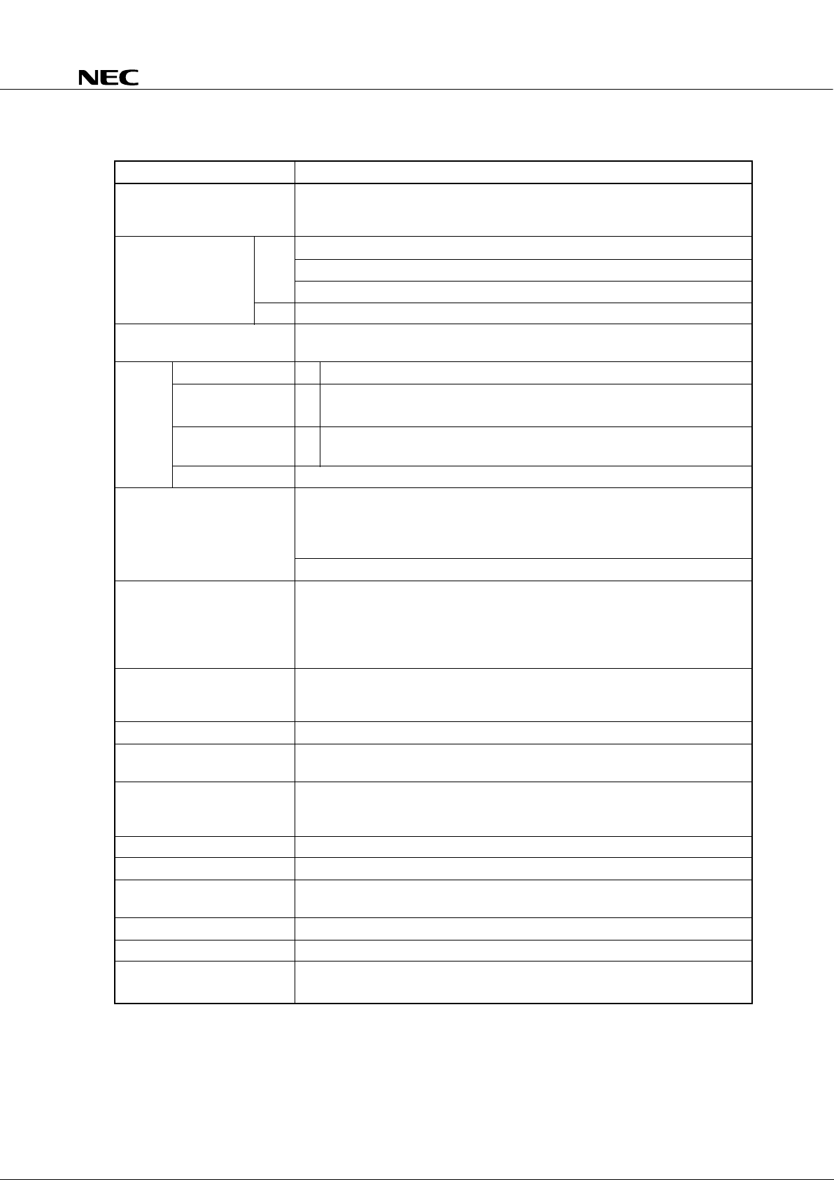
Functional Outline
Parameter Function
Instruction execution time • 0.95, 1.91, 3.81, 15.3 µs (@ 4.19 MHz with main system clock)
• 0.67, 1.33, 2.67, 10.7 µs (@ 6.0 MHz with main system clock)
• 122 µs (@ 32.768 kHz with subsystem clock)
On-chip memory ROM 4096 x 8 bits (µPD753104)
6144 x 8 bits (µPD753106)
8192 x 8 bits (µPD753108)
RAM 512 x 4 bits
General-purpose register • 4-bit operation: 8 x 4 banks
• 8-bit operation: 4 x 4 banks
Input/ CMOS input 8 On-chip pull-up resistors which can be specified by software: 7
output
CMOS input/output 20 On-chip pull-up resistors which can be specified by software: 12
port
Also used for segment pins: 8
N-ch open-drain 4 On-chip pull-up resistors which can be specified by mask option, 13-V withstand
input/output pins voltage
Total 32
LCD controller/driver • Segment selection: 16/20/24 segments (can be changed to CMOS input/
output port in 4 time-unit; max. 8)
• Display mode selection: Static, 1/2 duty (1/2 bias), 1/3 duty (1/2 bias),
1/3 duty (1/3 bias), 1/4 duty (1/3 bias)
• On-chip split resistor for LCD drive can be specified by mask option
Timer 5 channels
• 8-bit timer/event counter: 3 channels (16-bit timer/event counter, carrier generator,
timer with gate)
• Basic interval timer/watchdog timer: 1 channel
• Watch timer: 1 channel
Serial interface • 3-wire serial I/O mode ... MSB or LSB can be selected for transferring first bit
• 2-wire serial I/O mode
• SBI mode
Bit sequential buffer (BSB) 16 bits
Clock output (PCL) • Φ, 524, 262, 65.5 kHz (@ 4.19 MHz with main system clock)
• Φ, 750, 375, 93.8 kHz (@ 6.0 MHz with main system clock)
Buzzer output (BUZ) • 2, 4, 32 kHz (@ 4.19 MHz with main system clock or
@ 32.768 kHz with subsystem clock)
• 2.93, 5.86, 46.9 kHz (@ 6.0 MHz with main system clock)
Vectored interrupt External: 3, Internal: 5
Test input External: 1, Internal: 1
System clock oscillator • Ceramic or crystal oscillator for main system clock oscillation
• Crystal oscillator for subsystem clock oscillation
Standby function STOP/HALT mode
Supply voltage VDD = 1.8 to 5.5 V
Package • 64-pin plastic QFP (14 x 14 mm, 0.8-mm pitch)
• 64-pin plastic QFP (12 x 12 mm, 0.65-mm pitch)

4
µ
PD753104, 753106, 753108
CONTENTS
1. PIN CONFIGURATION (Top View) ......................................................................................................6
2. BLOCK DIAGRAM................................................................................................................................8
3. PIN FUNCTIONS ...................................................................................................................................9
3.1 Port Pins ......................................................................................................................................9
3.2 Non-port Pins ............................................................................................................................11
3.3 Pin Input/Output Circuits .........................................................................................................13
3.4 Recommended Connections for Unused Pins.......................................................................15
4. SWITCHING FUNCTION BETWEEN Mk I MODE AND Mk II MODE ................................................16
4.1 Difference between Mk I Mode and Mk II Mode......................................................................16
4.2 Setting Method of Stack Bank Select Register (SBS) ...........................................................17
5. MEMORY CONFIGURATION .............................................................................................................18
6. PERIPHERAL HARDWARE FUNCTION ...........................................................................................23
6.1 Digital I/O Port...........................................................................................................................23
6.2 Clock Generator ........................................................................................................................23
6.3 Subsystem Clock Oscillator Control Functions ....................................................................25
6.4 Clock Output Circuit .................................................................................................................26
6.5 Basic Interval Timer/Watchdog Timer.....................................................................................27
6.6 Watch Timer ..............................................................................................................................28
6.7 Timer/Event Counter.................................................................................................................29
6.8 Serial Interface ..........................................................................................................................33
6.9 LCD Controller/Driver ...............................................................................................................35
6.10 Bit Sequential Buffer ................................................................................................................37
7. INTERRUPT FUNCTION AND TEST FUNCTION ..............................................................................38
8. STANDBY FUNCTION ........................................................................................................................40
9. RESET FUNCTION .............................................................................................................................41
10. MASK OPTION ...................................................................................................................................44
11. INSTRUCTION SET ............................................................................................................................45
12. ELECTRICAL SPECIFICATIONS.......................................................................................................59
13. CHARACTERISTIC CURVES (FOR REFERENCE ONLY) ...............................................................75
14. PACKAGE DRAWINGS .....................................................................................................................78
15. RECOMMENDED SOLDERING CONDITIONS .................................................................................80
5
µ
PD753104, 753106, 753108
APPENDIX A. µPD75308B, 753108 AND 75P3116 FUNCTIONAL LIST..............................................81
APPENDIX B. DEVELOPMENT TOOLS .................................................................................................83
APPENDIX C. RELATED DOCUMENTS ................................................................................................87
6
µ
PD753104, 753106, 753108
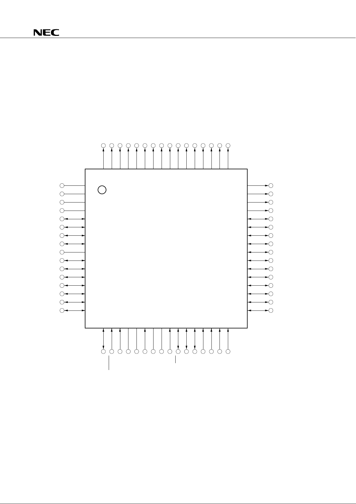
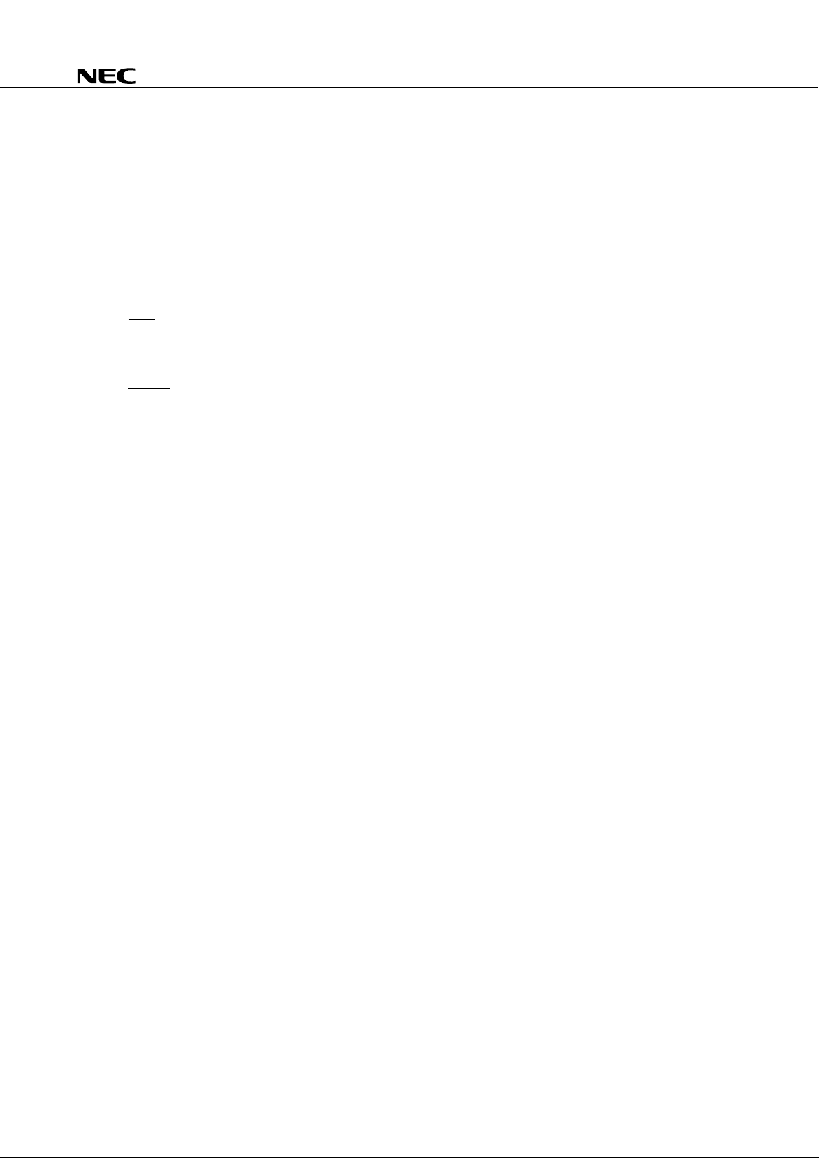
1. PIN CONFIGURATION (Top View)
• 64-pin plastic QFP (14 x 14 mm, 0.8-mm pitch)
µ
PD753104GC-xxx-AB8, µPD753106GC-xxx-AB8,
µ
PD753108GC-xxx-AB8
• 64-pin plastic QFP (12 x 12 mm, 0.65-mm pitch)
µ
PD753104GK-xxx-8A8, µPD753106GK-xxx-8A8,
µ
PD753108GK-xxx-8A8
Note Connect the IC (Internally Connected) pin directly to V
DD.
1
2
3
4
5
6
7
8
9
10
11
12
13
14
15
16
48
47
46
45
44
43
42
41
40
39
38
37
36
35
34
33
17
18
19
20
21
22
23
24
25
26
27
28
29
30
31
32
64
63
62
61
60
59
58
57
56
55
54
53
52
51
50
49
BIAS
V
LC0
V
LC1
V
LC2
P30/LCDCL
P31/SYNC
P32
P33
V
SS
P50
P51
P52
P53
P60/KR0
P61/KR1
P62/KR2
S12
S13
S14
S15
S16/P93
S17/P92
S18/P91
S19/P90
S20/P83
S21/P82
S22/P81
S23/P80
P23/BUZ
P22/PCL/PTO2
P21/PTO1
P20/PTO0
COM3
COM2
COM1
COM0
S0
S1
S2
S3
S4
S5
S6
S7
S8
S9
S10
S11
P63/KR3
RESET
XT1
XT2
IC
Note
X1
X2
V
DD
P00/INT4
P01/SCK
P02/SO/SB0
P03/SI/SB1
P10/INT0
P11/INT1
P12/INT2/TI1/TI2
P13/TI0
7
µ
PD753104, 753106, 753108
Pin Identification
P00 to P03 : Port 0 VLC0 to VLC2 : LCD Power Supply 0 to 2
P10 to P13 : Port 1 BIAS : LCD Power Supply Bias Control
P20 to P23 : Port 2 LCDCL : LCD Clock
P30 to P33 : Port 3 SYNC : LCD Synchronization
P50 to P53 : Port 5 TI0 to TI2 : Timer Input 0 to 2
P60 to P63 : Port 6 PTO0 to PTO2 : Programmable Timer Output 0 to 2
P80 to P83 : Port 8 BUZ : Buzzer Clock
P90 to P93 : Port 9 PCL : Programmable Clock
KR0 to KR3 : Key Return 0 to 3 INT0, INT1, INT4 : External Vectored Interrupt 0, 1, 4
SCK : Serial Clock INT2 : External Test Input 2
SI : Serial Input X1, X2 : Main System Clock Oscillation 1, 2
SO : Serial Output XT1, XT2 : Subsystem Clock Oscillation 1, 2
SB0, SB1 : Serial Data Bus 0, 1 V
DD : Positive Power Supply
RESET : Reset V
SS : Ground
S0 to S23 : Segment Output 0 to 23 IC : Internally Connected
COM0 to COM3 : Common Output 0 to 3
8
µ
PD753104, 753106, 753108
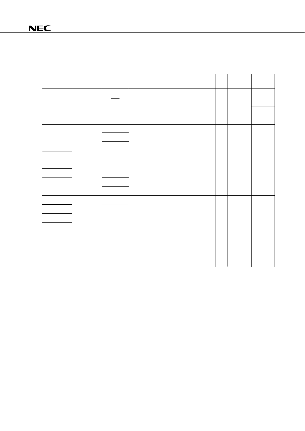
2. BLOCK DIAGRAM
Note The ROM capacity depends on the product.
WATCH
TIMER
INTW f
LCD
BASIC
INTERVAL
TIMER/
WATCHDOG
TIMER
INTBT
8-BIT
TIMER/EVENT
COUNTER #0
INTT0 TOUT0
8-BIT
TIMER/EVENT
COUNTER #1
8-BIT
TIMER/EVENT
COUNTER #2
CASCADED
16-BIT
TIMER/
EVENT
COUNTER
INTT2
CLOCKED
SERIAL
INTERFACE
INTCSI TOUT0
INT1
INTERRUPT
CONTROL
BIT SEQ.
BUFFER (16)
INT0/P10
INT1/P11
INT4/P00
INT2/P12/TI1/TI2
KR0/P60 to
KR3/P63
4
SI/SB1/P03
SO/SB0/P02
SCK/P01
TI1/TI2/P12/INT2
PTO1/P21
PTO2/PCL/P22
INTT1
TI0/P13
PTO0/P20
BUZ/P23
PROGRAM
COUNTER
PROGRAM
MEMORY
Note
(ROM)
ALU
DECODE
AND
CONTROL
CY
SP(8)
SBS
BANK
GENERAL REG.
DATA MEMORY
(RAM)
512 x 4 BITS
CLOCK
OUTPUT
CONTROL
CLOCK
DIVIDER
SYSTEM CLOCK
GENERATOR
MAIN SUB
STAND BY
CONTROL
CPU
CLOCK Φ
PCL/PTO2/P22 X1 X2 XT1XT2
IC V
DD
V
SS
RESET
f
LCD
PORT0 4 P00 to P03
PORT1 P10 to P13
PORT2 P20 to P23
PORT3 P30 to P33
PORT5 P50 to P53
PORT6 P60 to P63
PORT8 P80 to P83
PORT9 P90 to P93
LCD
CONTROLLER/
DRIVER
16 S0 to S15
4
S16/P93 to
S19/P904S20/P83 to
S23/P80
4 COM0 to COM3
BIAS
V
LC0
V
LC1
V
LC2
SYNC/P31
LCDCL/P30
f
x
/2
N
4
4
4
4
4
4
4
TOUT0
9
µ
PD753104, 753106, 753108
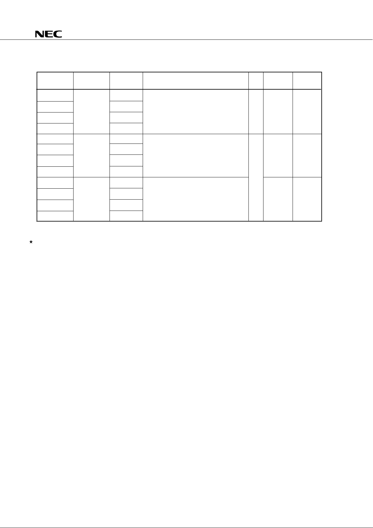
3. PIN FUNCTIONS
3.1 Port Pins (1/2)
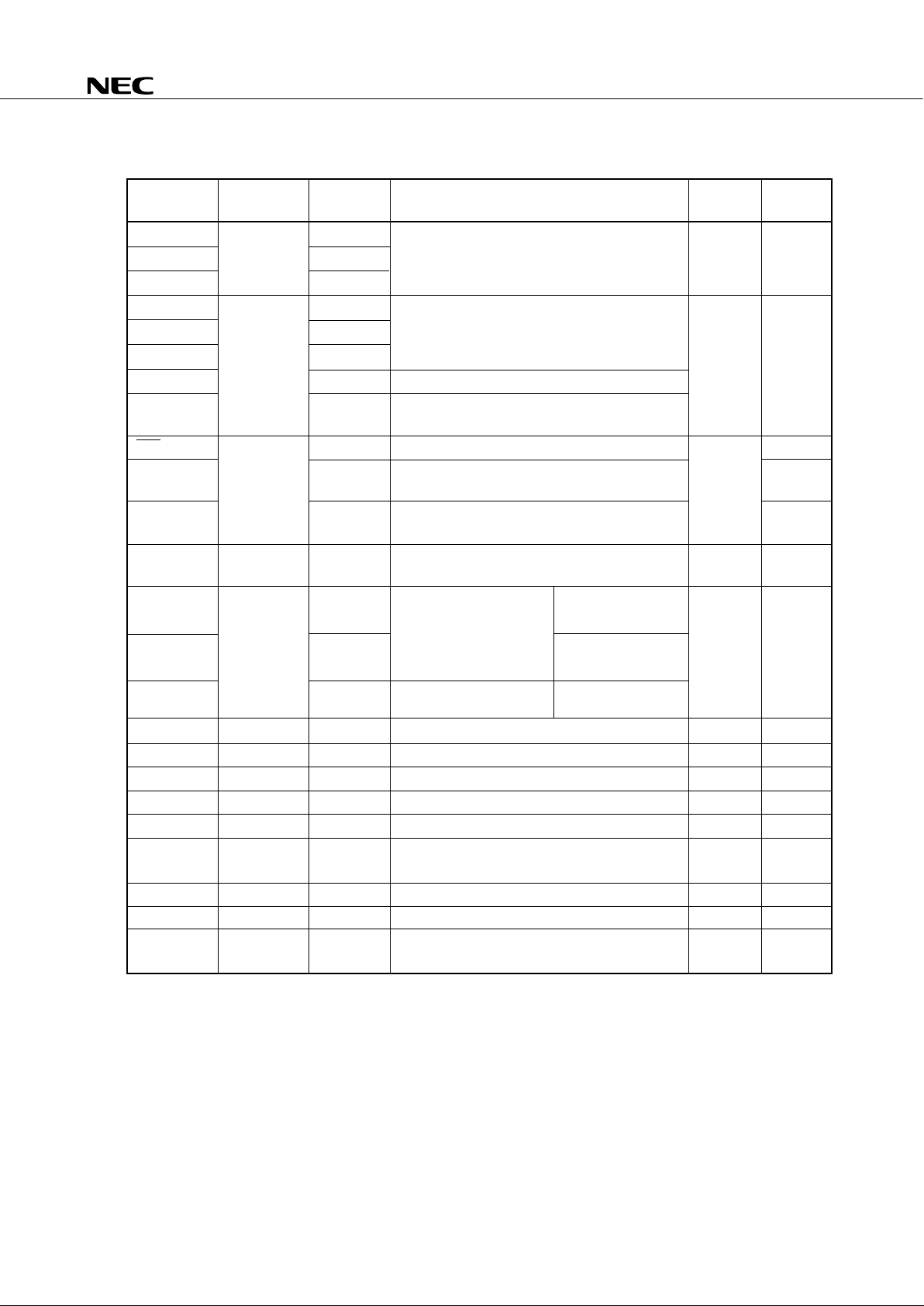
Pin Name Input/Output
Alternate
Function
8-bit
After Reset
I/O Circuit
Function I/O TYPE
Note 1
P00 Input INT4 No Input (B)
P01 Input/Output SCK (F)-A
P02 Input/Output SO/SB0 (F)-B
P03 Input/Output SI/SB1 (M)-C
P10 Input INT0 No Input (B)-C
P11 INT1
P12
TI1/TI2/INT2
P13 TI0
P20 Input/Output PTO0 No Input E-B
P21 PTO1
P22 PCL/PTO2
P23 BUZ
P30 Input/Output LCDCL No Input E-B
P31 SYNC
P32 –
P33 –
P50-P53
Note 2
Input/Output – No M-D
Notes 1. Characters in parentheses indicate the Schmitt trigger input.
2. If on-chip pull-up resistors are not specified by mask option (when used as N-ch open-drain input port),
low-level input leakage current increases when input or bit manipulation instruction is executed.
4-bit input port (PORT0).
For P01 to P03, connection of on-chip pullup resistors can be specified by software in
3-bit units.
4-bit input port (PORT1).
Connection of on-chip pull-up resistors can
be specified by software in 4-bit units.
P10/INT0 can select noise elimination
circuit.
4-bit input/output port (PORT2).
Connection of on-chip pull-up resistors can
be specified by software in 4-bit units.
Programmable 4-bit input/output port
(PORT3).
This port can be specified for input/output
bit-wise.
Connection of on-chip pull-up resistors can
be specified by software in 4-bit units.
N-ch open-drain 4-bit input/output port
(PORT5).
A pull-up resistor can be contained bit-wise
(mask option).
Withstand voltage is 13 V in open-drain mode.
High level
(when pullup resistors
are provided)
or highimpedance
10
µ
PD753104, 753106, 753108
3.1 Port Pins (2/2)
Pin Name Input/Output
Alternate
Function
8-bit
After Reset
I/O Circuit
Function I/O TYPE
Note 1
P60 Input/Output KR0 No Input (F)-A
P61 KR1
P62 KR2
P63 KR3
P80 Input/Output S23 Yes Input H
P81 S22
P82 S21
P83 S20
P90 Input/Output S19 Input H
P91 S18
P92 S17
P93 S16
Notes 1. Characters in parentheses indicate the Schmitt trigger input.
2. When these pins are used as segment signal output pins, do not connect the on-chip pull-up resistor
by software.
Programmable 4-bit input/output port
(PORT6).
This port can be specified for input/output
bit-wise.
Connection of on-chip pull-up resistors can
be specified by software in 4-bit units.
4-bit input/output port (PORT8).
Connection of on-chip pull-up resistors can
be specified by software in 4-bit units
Note 2
.
4-bit input/output port (PORT9).
Connection of on-chip pull-up resistors can
be specified by software in 4-bit units
Note 2
.
11
µ
PD753104, 753106, 753108
3.2 Non-port Pins (1/2)
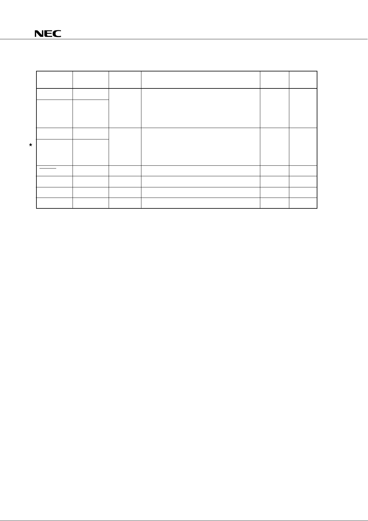
Pin Name Input/Output
Alternate
Function
After Reset
I/O Circuit
Function TYPE
Note 1
TI0 Input P13 Inputs external event pulses to the timer/event Input (B)-C
TI1
P12/INT2/TI2
counter.
TI2
P12/INT2/TI1
PTO0 Output P20 Timer/event counter output Input E-B
PTO1 P21
PTO2 P22/PCL
PCL P22/PTO2 Clock output
BUZ P23 Optional frequency output (for buzzer output or
system clock trimming)
SCK Input/Output P01 Serial clock input/output Input (F)-A
SO/SB0 P02 Serial data output (F)-B
Serial data bus input/output
SI/SB1 P03 Serial data input (M)-C
Serial data bus input/output
INT4 Input P00 Edge detection vectored interrupt input (both Input (B)
rising edge and falling edge detection)
INT0 Input P10 Input (B)-C
INT1 P11
INT2 P12/TI1/TI2
KR0-KR3 Input P60-P63 Falling edge detection testable input Input (F)-A
S0-S15 Output – Segment signal output Note 2 G-A
S16-S19 Output P93-P90 Segment signal output Input H
S20-S23 Output P83-P80 Segment signal output Input H
COM0-COM3 Output – Common signal output Note 2 G-B
VLC0-VLC2 – – LCD drive power – –
On-chip split resistor is enabled (mask option).
BIAS Output – Output for external split resistor disconnect Note 3 –
LCDCL
Note 4
Output P30 Clock output for externally expanded driver Input E-B
SYNC
Note 4
Output P31 Clock output for externally expanded driver Input E-B
synchronization
Notes 1. Characters in parentheses indicate the Schmitt trigger input.
2. Each display output selects the following V
LCX as input source.
S0-S15: V
LC1, COM0-COM2: VLC2, COM3: VLC0
3. When a split resistor is contained ........Low level
When no split resistor is contained ...... High-impedance
4. These pins are provided for future system expansion.
At present, these pins are used only as pins P30 and P31.
Edge detection vectored
Noise elimination circuit/
interrupt input (detection asynchronous selection
edge can be selected).
INT0/P10 can select noise
elimination circuit.
Rising edge detection
Asynchronous
testable input
Asynchronous
12
µ
PD753104, 753106, 753108
3.2 Non-port Pins (2/2)
Pin Name Input/Output
Alternate
Function
After Reset
I/O Circuit
Function TYPE
Note
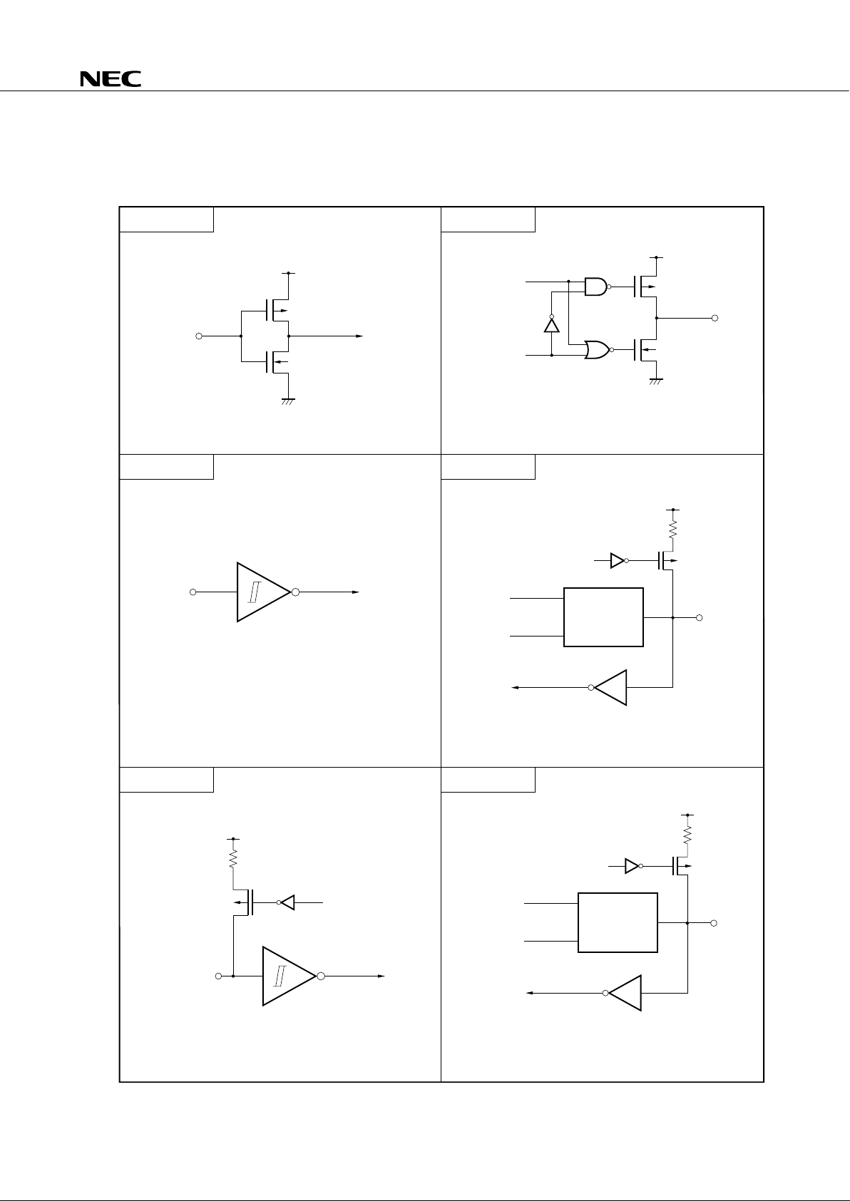
X1 Input – Crystal/ceramic connection pin for the main – –
system clock oscillation. When the external
clock is used, input the external clock to pin
X1, and the inverted phase of the external clock
to pin X2.
XT1 Input – – –
XT2 –
RESET Input – System reset input (low-level active) – (B)
IC – – Internally connected. Connect directly to V DD.– –
VDD – – Positive power supply – –
VSS – – Ground potential – –
Note Characters in parentheses indicate the Schmitt trigger input.
Crystal connection pin for the subsystem clock
oscillation. When the external clock is used, input
the external clock to pin XT1, and the inverted
phase of the external clock to pin XT2. Pin XT1 can
be used as a 1-bit input (test) pin.
X2 –
13
µ
PD753104, 753106, 753108
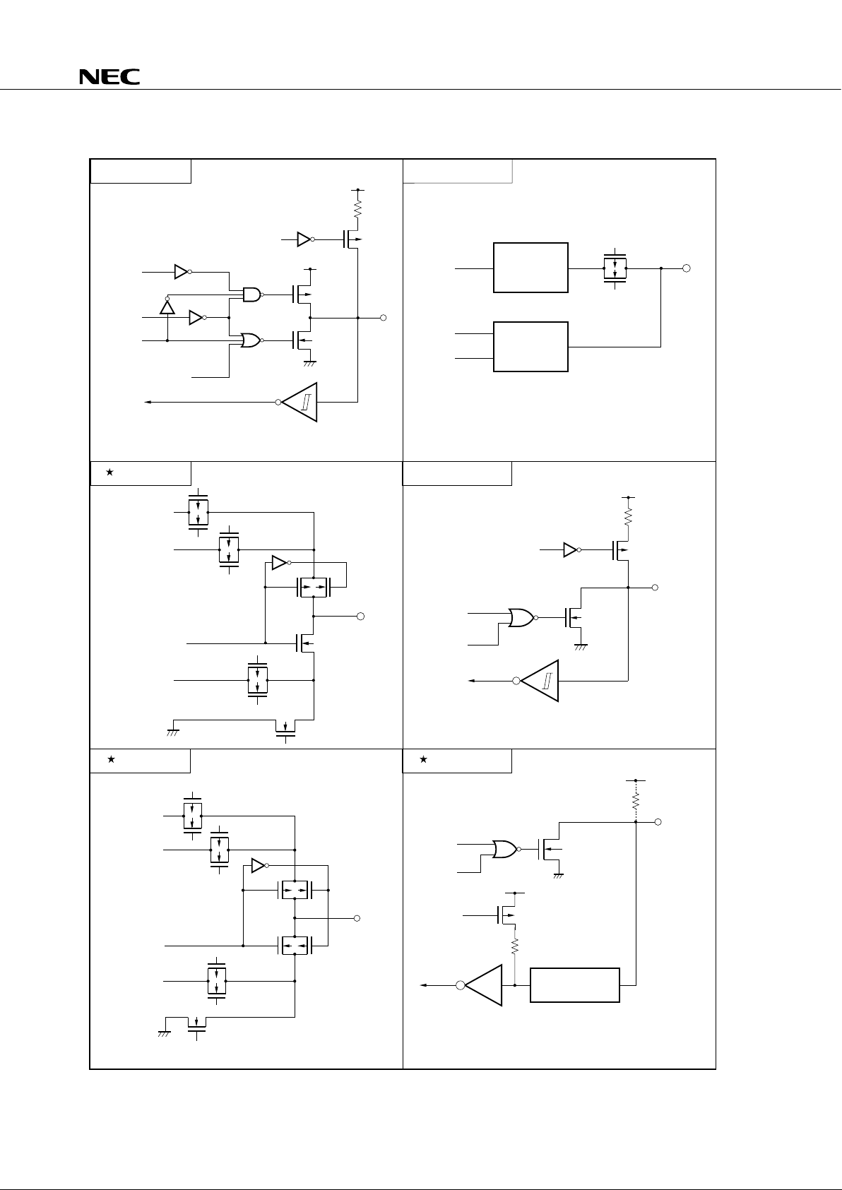
3.3 Pin Input/Output Circuits
The µPD753108 pin input/output circuits are shown schematically.
(1/2)
TYPE A
TYPE B
TYPE D
TYPE E-B
TYPE B-C
TYPE F-A
V
DD
IN
P-ch
N-ch
data
output
disable
N-ch
P-ch
IN
OUT
V
DD
P-ch
output
disable
data
P.U.R.
enable
Type D
Type A
IN/OUT
V
DD
P.U.R.
enable
P.U.R.
P-ch
IN
V
DD
P.U.R.
P.U.R.
enable
P-ch
IN/OUT
Type D
Type B
output
disable
data
P.U.R. : Pull-Up Resistor P.U.R. : Pull-Up Resistor
P.U.R. : Pull-Up Resistor
Schmitt trigger input with hysteresis characteristics
CMOS standard input buffer
Push-pull output that can be placed in output
high-impedance (both P-ch and N-ch off).
P.U.R.
V
DD
14
µ
PD753104, 753106, 753108
(2/2)
TYPE F-B TYPE H
TYPE G-A TYPE M-C
TYPE M-D
V
DD
P.U.R
enable
P.U.R.
P-ch
P-ch
V
DD
N-ch
output
disable
(P)
data
output
disable
output
disable
(N)
IN/OUT
P.U.R. : Pull-Up Resistor
data
output
disable
P.U.R.
enable
P.U.R.
V
DD
P-ch
IN/OUT
N-ch
P.U.R. : Pull-Up Resistor
TYPE G-B
SEG
data
data
output
disable
TYPE G-A
TYPE E-B
IN/OUT
N-ch
N-ch
V
LC0
V
LC1
SEG
data
V
LC2
OUT
P-ch
N-ch
P-ch
N-ch
P-ch
N-ch
N-chP-ch
V
LC0
V
LC1
P-ch N-ch
OUT
N-ch
V
LC2
N-ch
COM
data
P-ch
P-ch
N-ch
P-ch
N-ch
P-ch
N-ch
IN/OUT
P.U.R.
(Mask Option)
data
output
disable
N-ch
P-ch
input
instruction
(+13 V withstand
voltage)
The pull-up resistor operates only when an input
instruction is executed (current flows from V
DD
to
the pin when the pin is low).
V
DD
V
DD
P.U.R.
Voltage limitation
circuit
Note
(+13 V
withstand
voltage)
Note
15
µ
PD753104, 753106, 753108
3.4 Recommended Connections for Unused Pins
Table 3-1. List of Recommended Connections for Unused Pins
Pin Recommended Connection
P00/INT4 Connect to VSS or VDD
P01/SCK Connect to VSS or VDD via a resistor individually
P02/SO/SB0
P03/SI/SB1 Connect to VSS
P10/INT0, P11/INT1 Connect to VSS or VDD
P12/TI1/TI2/INT2
P13/TI0
P20/PTO0 Input state: Connect to VSS or VDD via a resistor
P21/PTO1 individually
P22/PCL/PTO2 Output state: Leave open
P23/BUZ
P30/LCDCL
P31/SYNC
P32
P33
P50-P53 Input state: Connect to VSS
Output state: Connect to VSS (do not connect a
pull-up resistor of mask option)
P60/KR0-P63/KR3 Input state: Connect to VSS or VDD via a resistor
individually
Output state: Leave open
S0-S15 Leave open
COM0-COM3
S16/P93-S19/P90
Input state: Connect to V
SS or VDD via a resistor
individually
S20/P83-S23/P80
Output state: Leave open
V
LC0-VLC2 Connect to VSS
BIAS Only if all of VLC0 to VLC2 are unused, connect to VSS.
In other cases, leave open.
XT1
Note
Connect to VSS or VDD
XT2
Note
Leave open
IC Connect directly to VDD
Note When the subsystem clock is not used, specify SOS.0 = 1 (so as not
to use the on-chip feedback resistor).
16
µ
PD753104, 753106, 753108
4. SWITCHING FUNCTION BETWEEN Mk I MODE AND Mk II MODE
4.1 Difference between Mk I Mode and Mk II Mode
The CPU of the µPD753108 has the following two modes: Mk I and Mk II, either of which can be selected. The
mode can be switched by bit 3 of the stack bank select register (SBS).
• Mk I mode: Upward compatible with the
µ
PD75308B. Can be used in the 75XL CPU with a ROM capacity
of up to 16 Kbytes.
• Mk II mode: Incompatible with the
µ
PD75308B. Can be used in all the 75XL CPU’s including those products
whose ROM capacity is more than 16 Kbytes.
Table 4-1. Differences between Mk I Mode and Mk II Mode
Mk I mode Mk II mode
Number of stack bytes 2 bytes 3 bytes
for subroutine instructions
BRA !addr1 instruction Not available Available
CALLA !addr1 instruction
CALL !addr instruction 3 machine cycles 4 machine cycles
CALLF !faddr instruction 2 machine cycles 3 machine cycles
Caution The Mk II mode supports a program area exceeding 16 Kbytes for the 75X and 75XL
Series. Therefore, this mode is effective for enhancing software compatibility with
products exceeding 16 Kbytes.
When the Mk II mode is selected, the number of stack bytes used during execution of
subroutine call instructions increases by one byte per stack compared to the Mk I mode.
When the CALL !addr and CALLF !faddr instructions are used, the machine cycle
becomes longer by one machine cycle. Therefore, use the Mk I mode if the RAM
efficiency and processing performance are more important than software compatibility.
17
µ
PD753104, 753106, 753108
Caution Since SBS. 3 is set to “1” after a RESET signal is generated, the CPU operates in the Mk
I mode. When executing an instruction in the Mk II mode, set SBS. 3 to “0” to select the
Mk II mode.
4.2 Setting Method of Stack Bank Select Register (SBS)
Switching between the Mk I mode and Mk II mode can be done by the stack bank select register (SBS). Figure
4-1 shows the format.
The SBS is set by a 4-bit memory manipulation instruction.
When using the Mk I mode, the SBS must be initialized to 100xB
Note
at the beginning of a program. When using
the Mk II mode, it must be initialized to 000xB
Note
.
Note Set the desired value in the x position.
Figure 4-1. Stack Bank Select Register Format
SBS3 SBS2 SBS1 SBS0
3210
Symbol
SBS
Address
F84H
00
01
0
1
0
Memory bank 0
Memory bank 1
Other than above setting prohibited
0 must be set in the bit 2 position.
Stack area specification
Mk II mode
Mk I mode
Mode switching specification
18
µ
PD753104, 753106, 753108
5. MEMORY CONFIGURATION
Program Memory (ROM) .... 4096 x 8 bits (µPD753104)
.... 6144 x 8 bits (
µ
PD753106)
.... 8192 x 8 bits (
µ
PD753108)
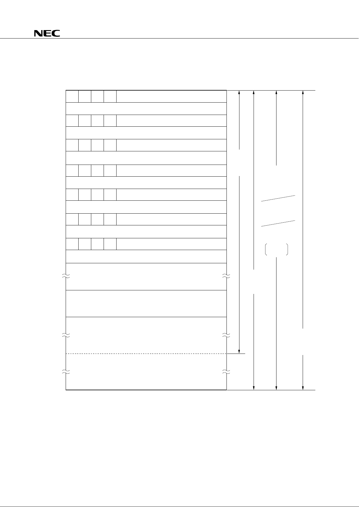
• Addresses 0000H and 0001H
Vector table wherein the program start address and the values set for the RBE and MBE at the time a
RESET signal is generated are written. Reset start is possible from any address.
• Addresses 0002H to 000DH
Vector table wherein the program start address and the values set for the RBE and MBE by each vectored
interrupt are written. Interrupt processing can start from any address.
• Addresses 0020H to 007FH
Table area referenced by the GETI instruction
Note
.
Note The GETI instruction realizes a 1-byte instruction on behalf of any 2-byte instruction, 3-byte
instruction, or two 1-byte instructions. It is used to decrease the number of program steps.
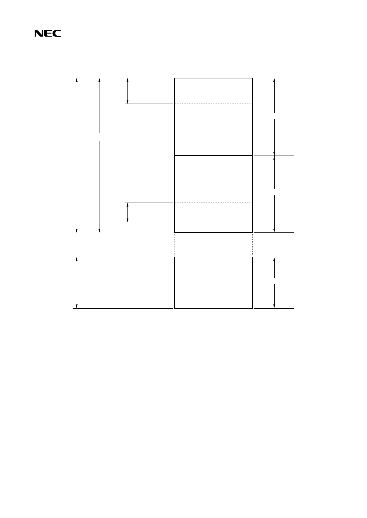
Data Memory (RAM)
• Data area ... 512 words x 4 bits (000H to 1FFH)
• Peripheral hardware area ... 128 words x 4 bits (F80H to FFFH)
19
µ
PD753104, 753106, 753108
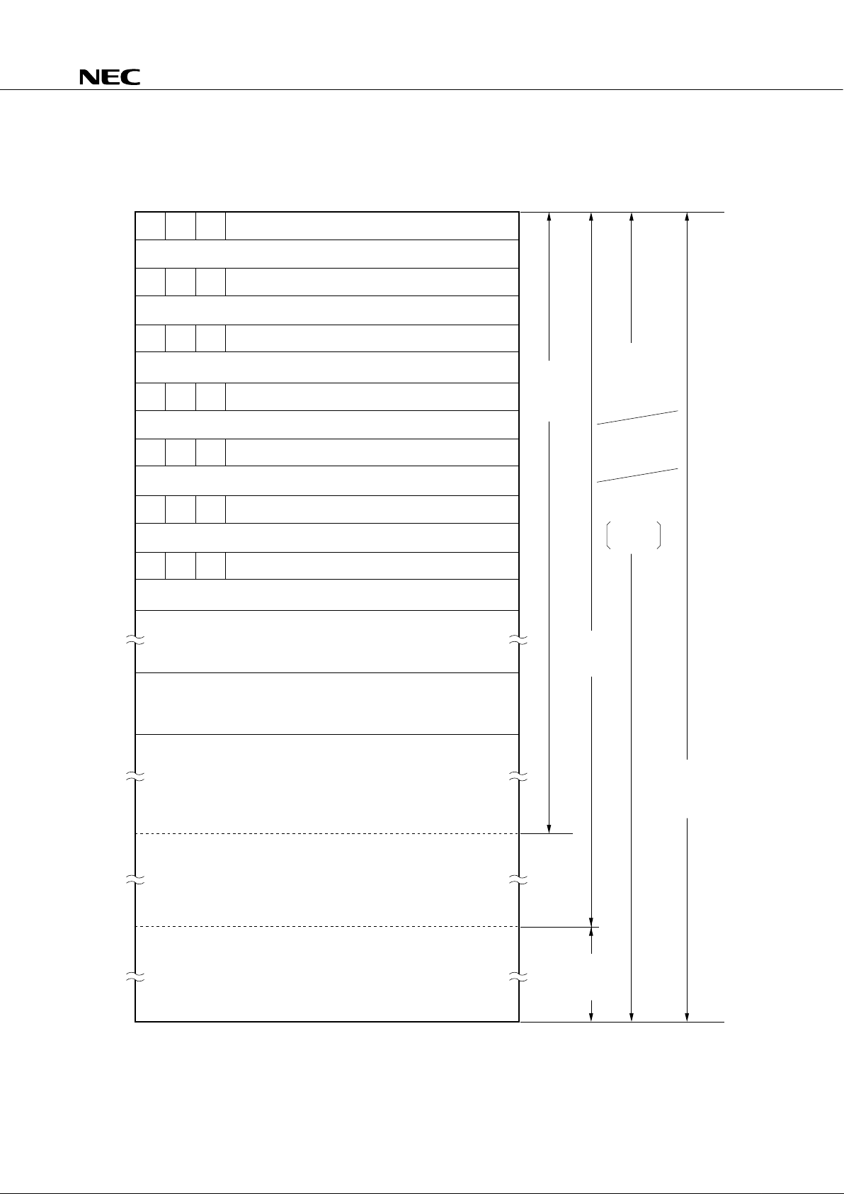
Figure 5-1. Program Memory Map (1/3)
(a)
µ
PD753104
Note Can be used in Mk II mode only.
Remark In addition to the above, a branch can be taken to the address indicated by changing only the low-order
eight bits of PC by executing the BR PCDE or BR PCXA instruction.
000H
Address
7654
MBE RBE 0 0 Internal reset start address (high-order 4 bits)
0
002H MBE RBE 0 0 INTBT/INT4 (high-order 4 bits)start address
004H MBE RBE 0 0 INT0 (high-order 4 bits)start address
006H MBE RBE 0 0 INT1 (high-order 4 bits)start address
008H MBE RBE 0 0 INTCSI (high-order 4 bits)start address
00AH MBE RBE 0 0 INTT0 (high-order 4 bits)start address
00CH MBE RBE 0 0 INTT1/INTT2 (high-order 4 bits)start address
020H
07FH
080H
7FFH
800H
FFFH
GETI instruction reference table
(low-order 8 bits)
(low-order 8 bits)
(low-order 8 bits)
(low-order 8 bits)
(low-order 8 bits)
(low-order 8 bits)
(low-order 8 bits)
CALLF
!faddr
instruction
entry
address
BRCB !caddr
instruction
branch
address
Branch destination
address and
subroutine entry
address when GETI
instruction is executed
Internal reset start address
INTBT/INT4 start address
INT0 start address
INT1 start address
INTCSI start address
INTT0 start address
INTT1/INTT2 start address
Branch address
of BR BCXA, BR
BCDE, BR !addr,
BRA !addr1
Note
or
CALLA !addr1
Note
instruction
CALL !addr
instruction
subroutine entry
address
BR $addr
instruction relative
branch address
–15 to –1,
+2 to +16
20
µ
PD753104, 753106, 753108
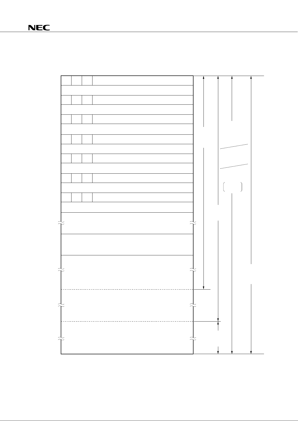
Figure 5-1. Program Memory Map (2/3)
(b)
µ
PD753106
Note Can be used in Mk II mode only.
Remark In addition to the above, a branch can be taken to the address indicated by changing only the low-order
eight bits of PC by executing the BR PCDE or BR PCXA instruction.
0000H
Address
0002H MBE RBE 0 INTBT/INT4 (high-order 5 bits)start address
0004H MBE RBE 0 INT0 (high-order 5 bits)start address
0006H MBE RBE 0 INT1 (high-order 5 bits)start address
0008H MBE RBE 0 INTCSI (high-order 5 bits)start address
000AH MBE RBE 0 INTT0 (high-order 5 bits)start address
0020H
007FH
0080H
07FFH
0800H
MBE RBE 0
Internal reset start address (high-order 5 bits)
0FFFH
1000H
17FFH
GETI instruction reference table
000CH MBE RBE 0 INTT1/INTT2 (high-order 5 bits)start address
(low-order 8 bits)
(low-order 8 bits)
(low-order 8 bits)
(low-order 8 bits)
(low-order 8 bits)
(low-order 8 bits)
(low-order 8 bits)
CALLF
!faddr
instruction
entry
address
BRCB !caddr
instruction
branch
address
Branch address
of BR BCXA, BR
BCDE, BR !addr,
BRA !addr1
Note
or
CALLA !addr1
Note
instruction
CALL !addr
instruction
subroutine entry
address
BR $addr
instruction relative
branch address
–15 to –1,
+2 to +16
Branch destination
address and
subroutine entry
address when GETI
instruction is executed
BRCB !caddr
instruction
branch
address
765 0
Internal reset start address
INTBT/INT4
INT0
INT1
INTCSI
INTT0
INTT1/INTT2
start address
start address
start address
start address
start address
start address
21
µ
PD753104, 753106, 753108
Figure 5-1. Program Memory Map (3/3)
(c)
µ
PD753108
Note Can be used in Mk II mode only.
Remark In addition to the above, a branch can be taken to the address indicated by changing only the low-order
eight bits of PC by executing the BR PCDE or BR PCXA instruction.
0000H
Address
0002H MBE RBE 0 INTBT/INT4 (high-order 5 bits)start address
0004H MBE RBE 0 INT0 (high-order 5 bits)start address
0006H MBE RBE 0 INT1 (high-order 5 bits)start address
0008H MBE RBE 0 INTCSI (high-order 5 bits)start address
000AH MBE RBE 0 INTT0 (high-order 5 bits)start address
0020H
007FH
0080H
07FFH
0800H
MBE RBE 0
Internal reset start address (high-order 5 bits)
0FFFH
1000H
1FFFH
GETI instruction reference table
000CH MBE RBE 0 INTT1/INTT2 (high-order 5 bits)start address
(low-order 8 bits)
(low-order 8 bits)
(low-order 8 bits)
(low-order 8 bits)
(low-order 8 bits)
(low-order 8 bits)
(low-order 8 bits)
CALLF
!faddr
instruction
entry
address
BRCB !caddr
instruction
branch
address
Branch address
of BR BCXA, BR
BCDE, BR !addr,
BRA !addr1
Note
or
CALLA !addr1
Note
instruction
CALL !addr
instruction
subroutine entry
address
BR $addr
instruction relative
branch address
–15 to –1,
+2 to +16
Branch destination
address and
subroutine entry
address when GETI
instruction is executed
BRCB !caddr
instruction
branch
address
765 0
Internal reset start address
INTBT/INT4
INT0
INT1
INTCSI
INTT0
INTT1/INTT2
start address
start address
start address
start address
start address
start address
22
µ
PD753104, 753106, 753108
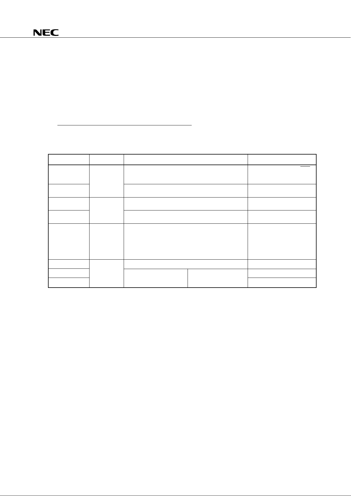
Figure 5-2. Data Memory Map
Note Either memory bank 0 or 1 can be selected for the stack area.
Data area
static RAM
(512 x 4)
Stack area
Note
General-purpose
register area
000H
01FH
0FFH
100H
1DFH
1E0H
1F7H
1F8H
1FFH
F80H
FFFH
Display data
memory
Peripheral hardware area
Data memory Memory bank
0
(32 x 4)
256 x 4
(224 x 4)
256 x 4
(224 x 4)
(24 x 4)
(8 x 4)
Not incorporated
128 x 4
15
1
23
µ
PD753104, 753106, 753108
6. PERIPHERAL HARDWARE FUNCTION
6.1 Digital I/O Port
There are three kinds of I/O port.
• CMOS input ports (PORT 0, 1) : 8
• CMOS input/output ports (PORT 2, 3, 6, 8, 9) : 20
• N-ch open-drain input/output ports (PORT 5) : 4
Total 32
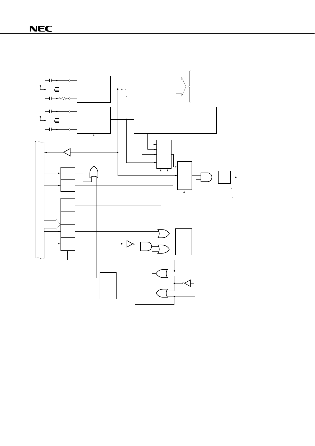
Table 6-1. Types and Features of Digital Ports
Port name Function Operation and features Remarks
PORT0 4-bit input When the serial interface function is used, the dual Also used for the INT4, SCK,
function pins function as output ports depending on the SO/SB0, SI/SB1 pins.
operation mode.
PORT1 4-bit input only port. Also used for the INT0-INT2/
TI1/TI2, TI0 pins.
PORT2 4-bit input/ Can be set to input mode or output mode in 4-bit units. Also used for the PTO0-
output PTO2/PCL, BUZ pins.
PORT3 Can be set to input mode or output mode bit-wise. Also used for the LCDCL,
SYNC pins.
PORT5 4-bit input/ Can be set to input mode or output mode in 4-bit units. —
output On-chip pull-up resistor can be specified bit-wise
(N-ch open- by mask option.
drain, 13 V
withstand
voltage)
PORT6 4-bit input/ Can be set to input mode or output mode bit-wise.
Also used for the KR0-KR3 pins.
PORT8
output
Can be set to input Ports 8 and 9 are paired
Also used for the S20-S23 pins.
PORT9
mode or output mode and data can be input/
Also used for the S16-S19 pins.
in 4-bit units. output in 8-bit units.
6.2 Clock Generator
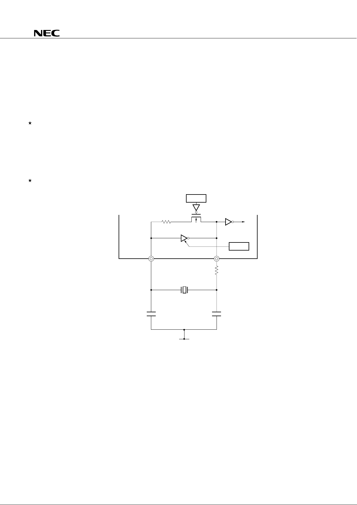
The clock generator is a device that generates the clock which is supplied to peripheral hardware on the CPU
and is configured as shown in Figure 6-1.
The clock generator operates according to how the processor clock control register (PCC) and system clock
control register (SCC) are set.
There are two kinds of clocks, main system clock and subsystem clock.
The instruction execution time can also be changed.
• 0.95, 1.91, 3.81, 15.3
µ
s (main system clock: in 4.19-MHz operation)
• 0.67, 1.33, 2.67, 10.7
µ
s (main system clock: in 6.0-MHz operation)
• 122
µ
s (subsystem clock: in 32.768-kHz operation)
24
µ
PD753104, 753106, 753108
Figure 6-1. Clock Generator Block Diagram
Note Instruction execution
Remarks 1. f
X = Main system clock frequency
2. f
XT = Subsystem clock frequency
3. Φ = CPU clock
4. PCC: Processor Clock Control Register
5. SCC: System Clock Control Register
6. One clock cycle (t
CY) of the CPU clock is equal to one machine cycle of the instruction.
V
DD
V
DD
XT1
X1
XT2
X2
f
XT
f
X
Subsystem
clock oscillator
Main system
clock oscillator
4
HALT
Note
STOP
Note
WM.3
SCC
SCC3
SCC0
PCC0
PCC1
PCC2
PCC3
PCC2,
PCC3
Clear
STOP F/F
Q
S
R
Oscillation
stop
HALT F/F
S
R
Wait release signal from BT
RESET signal
Standby release signal from
interrupt control circuit
· CPU
· INT0 noise
elimination circuit
· Clock output circuit
Φ
1/4
Divider
1/1 to 1/4096
Divider
1/21/4 1/16
· Basic interval timer (BT)
· Timer/event counter
· Serial interface
· Watch timer
· LCD controller/driver
· INT0 noise elimination circuit
· Clock output circuit
LCD controller/driver
Watch timer
PCC
Q
Selector
Selector
Internal bus
25
µ
PD753104, 753106, 753108
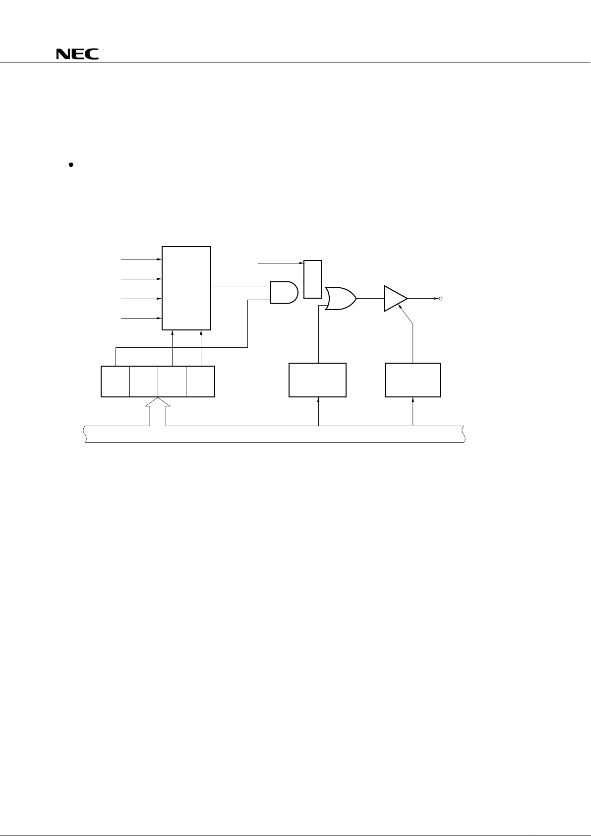
6.3 Subsystem Clock Oscillator Control Functions
The µPD753108 subsystem clock oscillator has the following two control functions.
• Selects by software whether an on-chip feedback resistor is to be used or not
Note
.
• Reduces current consumption by decreasing the drive current of the on-chip inverter when the supply voltage
is high (V
DD ≥ 2.7 V).
Note When the subsystem clock is not used, set SOS.0 to 1 (so as not to use the on-chip feedback resistor) by
software, connect XT1 to V
SS or VDD, and open XT2. This makes it possible to reduce the current
consumption in the subsystem clock oscillator.
The above functions can be used by switching the bits 0 and 1 of the sub-oscillator control register (SOS). (See
Figure 6-2.)
Figure 6-2. Subsystem Clock Oscillator
Feedback resistor
SOS.0
SOS.1
XT1 XT2
Inverter
V
DD
26
µ
PD753104, 753106, 753108
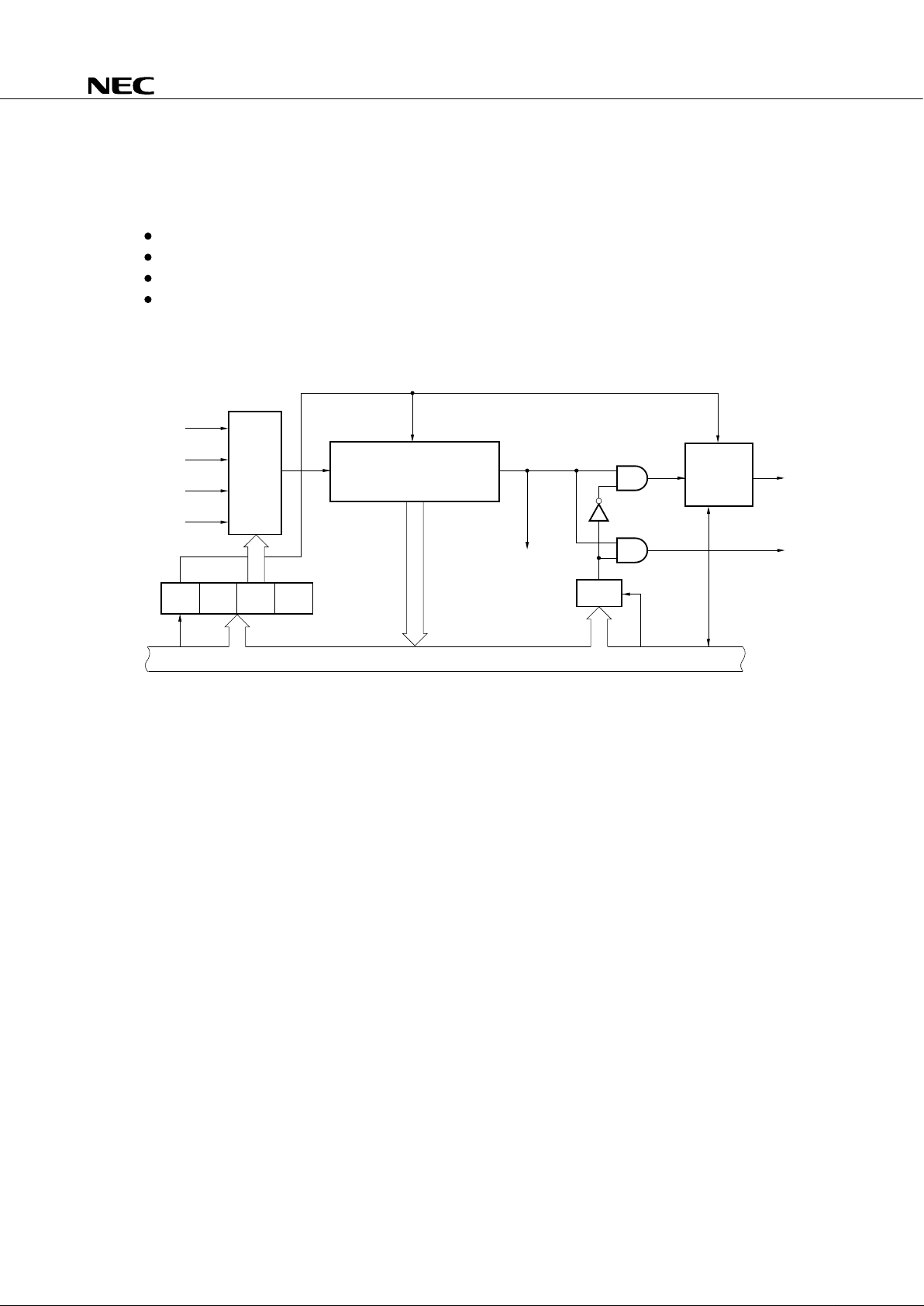
6.4 Clock Output Circuit
The clock output circuit is provided to output the clock pulses from the P22/PTO2/PCL pin to the remote control
wave outputs and peripheral LSI’s.
Clock output (PCL): Φ, 524, 262, 65.5 kHz (main system clock: in 4.19-MHz operation)
Φ, 750, 375, 93.8 kHz (main system clock: in 6.0-MHz operation)
Figure 6-3. Clock Output Circuit Block Diagram
Remark Special care has been taken in designing the chip so that small-width pulses may not be output
when switching clock output enable/disable.
From clock
generator
Φ
f
X/2
3
fX/2
4
fX/2
6
Selector
CLOM3 0 CLOM1 CLOM04CLOM
P22
output latch
Port 2 I/O mode
specification bit
PORT2.2 Bit 2 of PMGB
Internal bus
Output buffer
PCL/PTO2/P22
Selector
From timer/event
counter
(channel 2)
27
µ
PD753104, 753106, 753108
6.5 Basic Interval Timer/Watchdog Timer
The basic interval timer/watchdog timer has the following functions.
Interval timer operation to generate a reference time interrupt
Watchdog timer operation to detect a runaway of program and reset the CPU
Selects and counts the wait time when the standby mode is released
Reads the contents of counting
Figure 6-4. Basic Interval Timer/Watchdog Timer Block Diagram
Note Instruction execution
From clock
generator
f
X
/2
5
fX/2
7
fX/2
9
fX/2
12
MPX
BTM3 BTM2 BTM1 BTM0 BTM
4
SET1
Note
Internal bus
81
Basic interval timer
(8-bit frequency divider)
Clear
BT
Wait release signal
when standby is
released.
Set
Clear
3
WDTM
SET1
Note
Internal reset
signal
Vectored
interrupt
request signal
BT
interrupt
request flag
IRQBT
 Loading...