NEC UPD75238GJ-XXX-5BG Datasheet

Document No. IC-2777A
(O.D. No. IC-8177A)
Date Published February 1993 P
Printed in Japan
The information in this document is subject to change without notice.
DATA SHEET
MOS INTEGRATED CIRCUIT
µ
PD75238
4 BIT SINGLE-CHIP MICROCOMPUTER
The µPD75238 is a single-chip microcomputer which contains a CPU capable of 1-, 4-, and 8-bit data
processing, ROM, RAM, and I/O ports. In addition, it contains a fluorescent display tube (FIP
;
) controller/driver,
A/D converter, clock timer, timer/pulse generator capable of 14-bit PWM output, serial interface, and vectored
interrupt function.
In comparison with the
µ
PD75217, the µPD75238 has larger ROM and RAM capacity and has been enhanced
in such peripheral facilities as the display function of the FIP controller/driver, I/O ports, A/D converter, serial
interface.
The
µ
PD75238 finds best use in such applications as timer/tuner of VCRs from advanced type to common
type, configuration of one-chip system control microcomputer, advanced CD player, advanced microwave
ovens, etc.
With the
µ
PD75238, the µPD75P238, which is a PROM product, and various development tools including
IE-75001-R and assemblers are available. They can be used for evaluation during system development and
small-volume production.
FEATURES
• Mass-storage built-in ROM and RAM
• Program memory (ROM) : 32K × 8
• Data memory (RAM) : 1K × 4
• I/O port: 64 lines (excluding pins dedicated
to FIP)
• Minimum instruction execution time:
0.67
µ
s (at 6.0 MHz)
• Instruction execution time specification func-
tion to allow a wide range of operating
voltages
• Programmable FIP controller/driver contained
• Number of segments : 9 to 24 segments
• Number of digits : 9 to 16 digits
ORDERING INFORMATION
Part number Package Quality grade
µ
PD75238GJ-×××-5BG 94-pin plastic QFP (20 × 20 mm) Standard
Please refer to “Quality Grade on NEC Semiconductor Devices” (Document number IEI-1209) published by NEC
Corporation to know the specification of quality grade on the devices and its recommended applications.
• 8-bit A/D converter: 8 channels
• Enhanced timer/counter function: 5 channels
• 8-bit serial interface: 2 channels
• Application-oriented interrupt functions
• PROM version device:
µ
PD75P238
Major changes in this revision are indicated by stars (★) in the margins.
ELECTRON DEVICE
© NEC Corporation 1992

2
µ
PD75238
FUNCTIONS
Item
ROM: 32640 × 8 bits, RAM: 1024 × 4 bits
• Input : 16 lines
64 lines • I/O : 24 lines
• Output : 24 lines
• 0.67 µs/1.33 µs/2.67 µs/10.7 µs (at 6.0 MHz)
• 0.95 µs/1.91 µs/3.82 µs/15.3 µs (at 4.19 MHz)
• 122 µs (at 32.768 kHz)
• Number of segments : 9 to 24 segments
• Number of digits : 9 to 16 digits
• Dimmer function : 8 levels
• Pull-down resistors provided by mask option
• Key scan interrupt generator
• Basic interval timer : Usable as watchdog timer
• Timer/event counter
5 channels • Clock timer : With buzzer output function
• Timer/pulse generator : With 14-bit PWM output function
• Event counter
2 channels • SBI or 3-wire mode
• 3-wire mode
• Allows multiple hardware interrupts.
• Detection of both edges
• External interrupts : 3 • Detection edge programmable (with noise
elimination)
• Detection edge programmable
• External test input : 1 • Rising edge detection
• Timer/pulse generator
• Timer/event counter
• Internal interrupts : 5 • Basic interval timer
• Serial interface #0
• For key scanning
• Internal test inputs: 2 • Clock timer
• Serial interface #1
• Main system clock : 6.0 MHz, 4.19 MHz
• Subsystem clock : 32.768 kHz, standard
• High-voltage port : Pull-down resistor or open-drain output
• Ports 4 and 5 : Pull-up resistor
• Port 7 : Pull-down resistor
-40 to +85 °C
2.7 to 6.0 V (Data held in standby mode: 2.0 to 6.0 V)
94-pin plastic QFP (20 × 20 mm)
On-chip memory
I/O lines
(Excluding pins dedicated to FIP)
Instruction cycle
Fluorescent display tube (FIP)
controller/driver
Timer/counter
Serial interface
Interrupt
System clock oscillator
Mask option
Operating temperature
Operating voltage
Package
Function
3
µ
PD75238
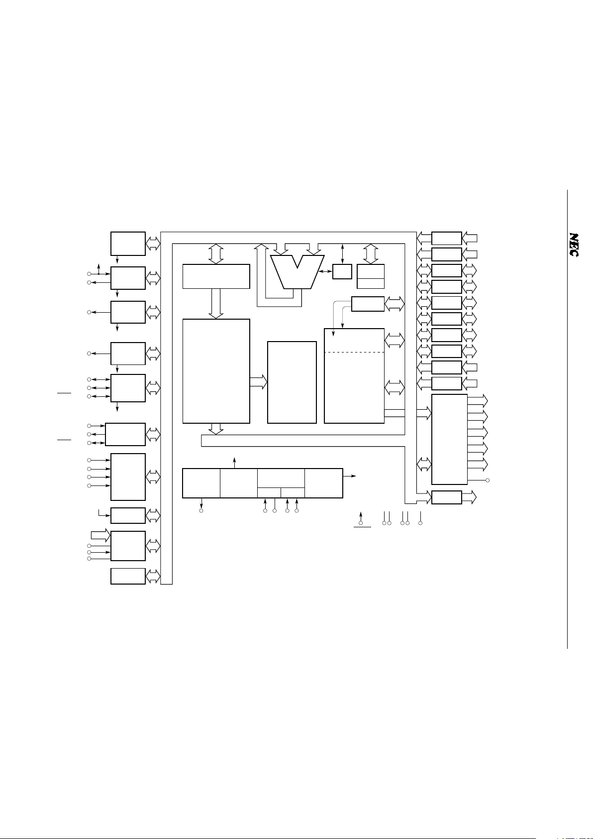
PIN CONFIGURATION
Caution Be sure to supply power to the AVDD, VDD, VSS, and AVSS pins (pins 3, 4, 5, 11, 30, 48, 65, and 87).
Remark IC: Internally connected pin (to be grounded)
AN1
PD75238GJ-×××-5BG
µ
AN2
AN3
AN4/P90
AN5/P91
AN6/P92
AN7/P93
AV
SS
P00/INT4
P02/SO0/SB0
P03/SI0/SB1
P10/INT0
P11/INT1
P12/INT2
P13/TI0
P20/PTO0
P21
P22/PCL
P23/BUZ
P30
P31
S5/P131
S6/P132
S7/P133
S8/P140
S9/P141
V
DD
V
LOAD
T15/S10/P142
T14/S11/P143
PH0/T13/S12/P150
PH1/T12/S13/P151
PH2/T11/S14/P152
PH3/T10/S15/P153
T9T8T7T6T5T4T3T2T1
T0
S4/P130
AN0
AV
REF
AV
DD
V
DD
V
DD
X2
X1
IC
XT2
XT1
V
SS
S16/P100
S17/P101
S18/P102
S19/P103
S20/P110
S21/P111
S22/P112
S23/P113
S0/P120
S1/P121
S2/P122
S3/P123
P33
P40
P41
P42
P43
V
SS
P50
P51
P52
P53
P60
P61
P62
P63
P70
P71
P72
P73
P80/PPO
P82/SO1
P83/SI1
V
DD
P32
94
939291 9089 8887 868584 8382 81807978 77767574 73
72
71
70
69
68
67
66
65
64
63
62
61
60
59
58
57
56
55
54
53
52
51
50
49
48
252627 2829 30 313233 34353637 38394041 424344 4546 47
1
2
3
4
5
6
7
8
9
10
11
12
13
14
15
16
17
18
19
20
21
22
23
24
RESET
P01/SCK0
P81/SCK1
4
µ
PD75238
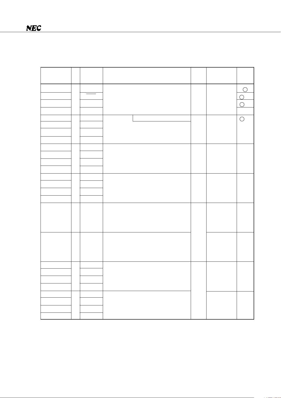
BLOCK DIAGRAM
fX/2
N
CPU clock
Φ
RESET V
SS
V
DD
PCL/P22 XT1XT2 X1 X2
V
DD
Port 0
Port 1
Port 2
Port 3
Port 4
Port 5
Port 6
Port 7
Port 8
Port 9
P00-P03
P10-P13
P20-P23
P30-P33
P40-P43
Note
P50-P53
Note
P60-P63
P70-P73
P80-P83
P90-P93
4
4
4
4
4
4
4
4
4
4
T0-T9
10
2
10
4
8
T10/S15/PH3/P153-
T13/S12/PH0/P150
T14/S11/P143 and
T15/S10/P142
S0/P120-S9/P141
S16/P100-S23/P113
V
LOAD
FIP
controller/
driver
24
Port 10-15 P100-P153
SP (8)
SBS (2)
CY
Bank
ALU
General register
RAM data
memory
Decode
and control
Program
counter (15)
ROM
program
memory
Stand by
control
Clock
generator
MainSub
Clock
divider
Clock
output
control
Basic
interval
timer
Timer/event
counter
#0
Watch
timer
INTBT
Timer/pulse
generator
INTT0
INTW
INTTPG
Serial
interface 0
INTCSI0
Serial
interface 1
Interrupt
control
Event
counter
A/D
converter
Bit sequential
buffer (16)
TI0
TI0/P13
PTO0/P20
BUZ/P23
PPO/P80
SI0/SB1/P03
SO0/SB0/P02
SCK0/P01
SI1/P83
SO1/P82
SCK1/P81
INT0/P10
INT1/P11
INT2/P12
INT4/P00
AN0-AN3
AN4/P90-AN7/P93
AV
DD
AV
REF
AV
SS
TI0
8
1024 × 4
32640 × 8
Note Port 4 and port 5 are N-ch open-drain I/O ports with a
medium withstand voltage of 10 V.

5
µ
PD75238
CONTENTS
1. PIN FUNCTIONS ........................................................................................................................ 7
1.1 PORT PINS ...................................................................................................................................... 7
1.2 NON-PORT PINS ............................................................................................................................ 9
1.3 PIN INPUT/OUTPUT CIRCUITS .................................................................................................... 11
1.4 CONNECTION OF UNUSED
µ
PD75238 PINS .............................................................................. 15
2. ARCHITECTURE AND MEMORY MAP OF THE µPD75238 ................................................... 16
2.1 DATA MEMORY BANK CONFIGURATION AND ADDRESSING MODES ................................ 16
2.2 GENERAL REGISTER BANK CONFIGURATION .......................................................................... 19
2.3 MEMORY-MAPPED I/O ................................................................................................................. 22
3. INTERNAL CPU FUNCTIONS.................................................................................................... 27
3.1 PROGRAM COUNTER (PC) ........................................................................................................... 27
3.2 PROGRAM MEMORY (ROM) ........................................................................................................ 27
3.3 DATA MEMORY (RAM) ................................................................................................................. 29
3.4 GENERAL REGISTERS ................................................................................................................... 31
3.5 ACCUMULATORS .......................................................................................................................... 32
3.6 STACK POINTER (SP) AND STACK BANK SELECT REGISTER (SBS) ..................................... 32
3.7 PROGRAM STATUS WORD (PSW) .............................................................................................. 35
3.8 BANK SELECT REGISTER (BS) ..................................................................................................... 39
4. PERIPHERAL HARDWARE FUNCTIONS .................................................................................. 40
4.1 DIGITAL I/O PORTS ....................................................................................................................... 40
4.2 CLOCK GENERATOR ...................................................................................................................... 49
4.3 CLOCK OUTPUT CIRCUIT ............................................................................................................. 58
4.4 BASIC INTERVAL TIMER ............................................................................................................... 61
4.5 TIMER/EVENT COUNTER ............................................................................................................. 63
4.6 CLOCK TIMER ................................................................................................................................. 69
4.7 TIMER/PULSE GENERATOR ......................................................................................................... 71
4.8 EVENT COUNTER .......................................................................................................................... 77
4.9 SERIAL INTERFACE ....................................................................................................................... 79
4.10 A/D CONVERTER ........................................................................................................................... 113
4.11 BIT SEQUENTIAL BUFFER ............................................................................................................ 119
4.12 FIP CONTROLLER/DRIVER ............................................................................................................ 119
5. INTERRUPT FUNCTION ............................................................................................................ 131
5.1 CONFIGURATION OF THE INTERRUPT CONTROL CIRCUIT .................................................... 131
5.2 HARDWARE OF THE INTERRUPT CONTROL CIRCUIT .............................................................. 133
5.3 INTERRUPT SEQUENCE ................................................................................................................ 138
5.4 MULTIPLE INTERRUPT PROCESSING CONTROL ...................................................................... 139
5.5 VECTOR ADDRESS SHARE INTERRUPT PROCESSING ............................................................ 141

6
µ
PD75238
6. STANDBY FUNCTION ............................................................................................................... 142
6.1 SETTING OF STANDBY MODES AND OPERATION STATUSES ............................................. 142
6.2 RELEASE OF THE STANDBY MODES ......................................................................................... 144
6.3 OPERATION AFTER A STANDBY MODE IS RELEASED ............................................................ 146
7. RESET FUNCTION ..................................................................................................................... 147
8. INSTRUCTION SET .................................................................................................................... 150
8.1
µ
PD75238 INSTRUCTIONS............................................................................................................ 150
8.2 INSTRUCTION SET AND ITS OPERATION .................................................................................. 153
8.3 INSTRUCTION CODES OF EACH INSTRUCTION ....................................................................... 162
9. SPECIFICATION OF MASK OPTIONS ...................................................................................... 168
10. APPLICATION BLOCK DIAGRAM ............................................................................................. 169
11. ELECTRICAL CHARACTERISTICS............................................................................................. 170
12. CHARACTERISTIC CURVES (FOR REFERENCE)..................................................................... 181
13. PACKAGE DIMENSIONS........................................................................................................... 183
14. RECOMMENDED SOLDERING CONDITIONS ......................................................................... 184
APPENDIX AµPD75238 SERIES PRODUCT FUNCTION LIST .................................................. 185
APPENDIX B DEVELOPMENT TOOLS......................................................................................... 186
★
7
µ
PD75238
1. PIN FUNCTIONS
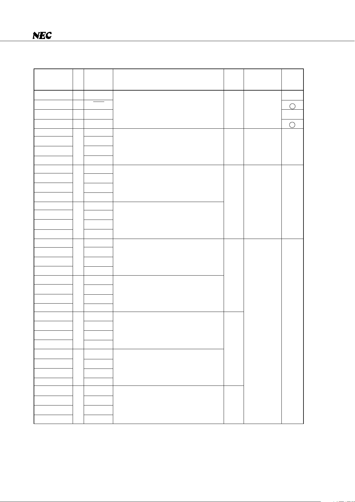
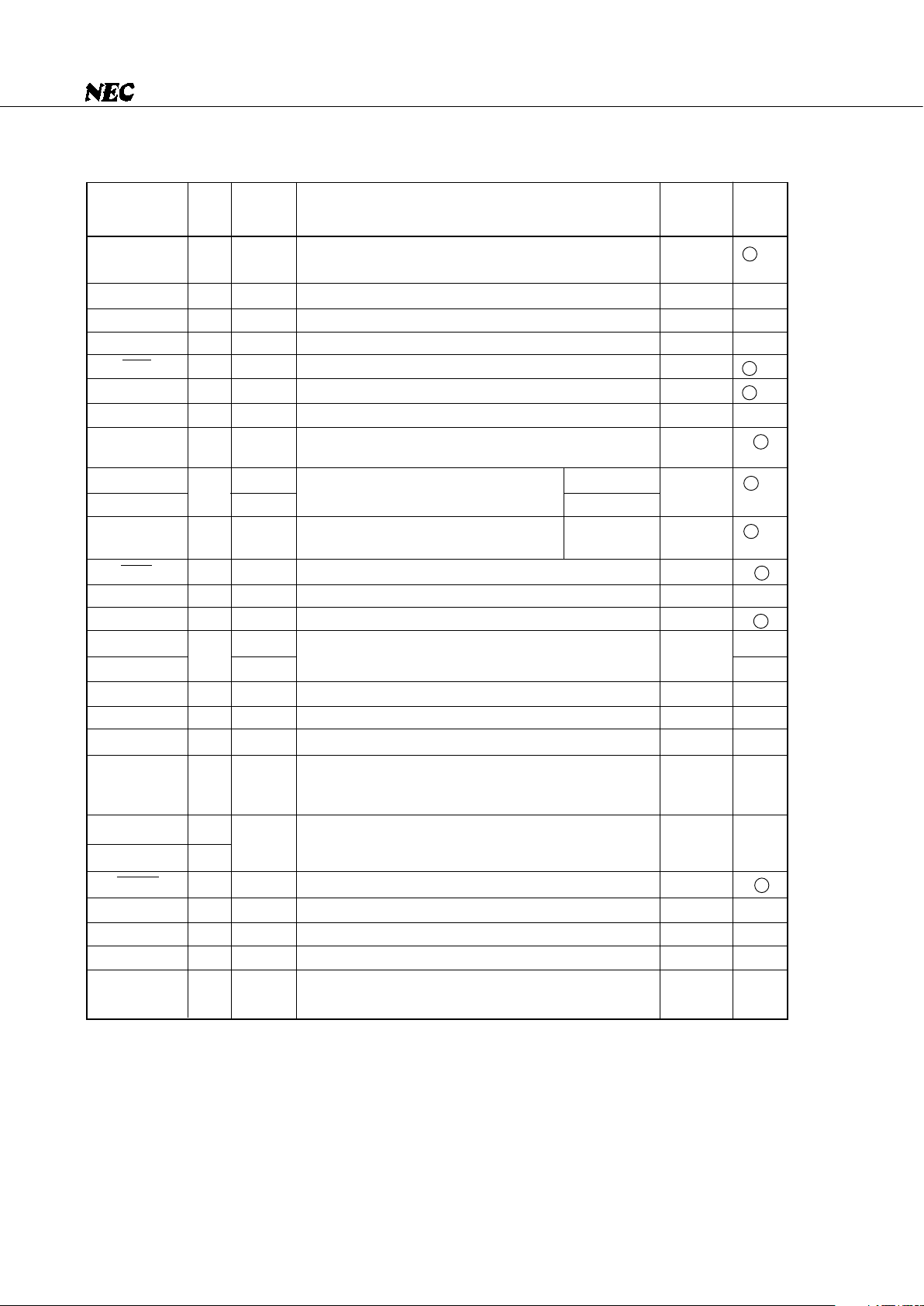
1.1 PORT PINS (1/2)
Notes 1. The circuits enclosed in circles have a Schmitt-triggered input.
2. An LED can be driven directly.
×
×
×
×
❍
❍
With noise elimination function
4-bit input port (port 0).
For P01 to P03, pull-up resistors can be
provided by software in units of 3 bits.
4-bit input port (port 1).
Pull-up resistors can be provided by software
in units of 4 bits.
4-bit I/O port (port 2).
Pull-up resistors can be provided by software
in units of 4 bits.
Programmable 4-bit I/O port (port 3).
Input/output can be specified bit by bit.
Pull-up resistors can be provided by software
in units of 4 bits.
N-ch open-drain 4-bit I/O port (port 4).
A pull-up resistor can be provided bit by bit
(mask option).
Withstand voltage is 10 V in open-drain mode.
N-ch open-drain 4-bit I/O port (port 5).
A pull-up resistor can be provided bit by bit
(mask option).
Withstand voltage is 10 V in open-drain mode.
Programmable 4-bit I/O port (port 6).
Input/output can be specified bit by bit.
Pull-up resistors can be provided by software
in units of 4 bits.
4-bit I/O port (port 7).
A pull-down resistor can be provided bit by bit
(mask option).
Pin name
B
F - A
F - B
M - C
B - C
E - B
E - C
M
M
E - C
V
Input
Input
Input
Input
High level
(when a pull-up
resistor is
provided) or
high impedance
High level
(when a pull-up
resistor is
provided) or
high impedance
Input
VSS level (when
a pull-down
resistor is
provided) or
high impedance
When resetFunction
I/O
Note 1
circuit
type
I
I
I/O
I/O
I/O
I/O
I/O
I/O
INT4
SCK0
SO0/SB0
SI0/SB1
INT0
INT1
INT2
TI0
PTO0
–
PCL
BUZ
–
–
–
–
–
–
–
–
–
–
–
–
–
–
Also
used as
I/O
P00
P01
P02
P03
P10
P11
P12
P13
P20
P21
P22
P23
P30
Note 2
P31
Note 2
P32
Note 2
P33
Note 2
P40-P43
Note 2
P50-P53
Note 2
P60
P61
P62
P63
P70
P71
P72
P73
8-bit I/O
8
µ
PD75238
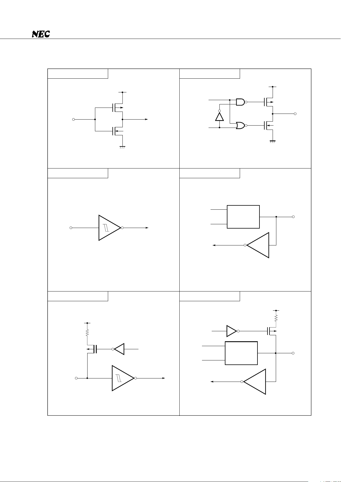
1.1 PORT PINS (2/2)
Note The circuits enclosed in circles have a Schmitt-triggered input.
×
×
❍
❍
❍
×
Function
8-bit I/O
When reset
A
F
E
B
Y - A
I - F
I - C
4-bit input port (port 8).
4-bit input port (port 9)
P-ch open-drain, 4-bit high-voltage output port.
Pull-down resistors can be provided (mask
option).
P-ch open-drain, 4-bit high-voltage output port.
Pull-down resistors can be provided (mask
option).
P-ch open-drain, 4-bit high-voltage output port.
Pull-down resistors can be provided (mask
option).
P-ch open-drain, 4-bit high-voltage output port.
Pull-down resistors can be provided (mask
option).
P-ch open-drain, 4-bit high-voltage output port.
Pull-down resistors can be provided (mask
option).
P142 and P143 can drive LED directly.
P-ch open-drain, 4-bit high-voltage output port.
Pull-down resistors can be provided (mask
option).
LED can be driven directly.
P-ch open-drain, 4-bit high-voltage output port.
Pull-down resistors can be provided (mask
option).
P80
P81
P82
P83
P90
P91
P92
P93
P100
P101
P102
P103
P110
P111
P112
P113
P120
P121
P122
P123
P130
P131
P132
P133
P140
P141
P142
P143
P150
P151
P152
P153
PH0
PH1
PH2
PH3
PPO
SCK1
SO1
SI1
AN4
AN5
AN6
AN7
S16
S17
S18
S19
S20
S21
S22
S23
S0
S1
S2
S3
S4
S5
S6
S7
S8
S9
S10/T15
S11/T14
S12/T13/PH0
S13/T12/PH1
S14/T11/PH2
S15/T10/PH3
S12/T13/P150
S13/T12/P151
S14/T11/P152
S15/T10/P153
Input
Input
VLOAD level
(when pulldown resistor
to VLOAD is
provided), VSS
level (when pulldown resistor to
VSS is pro-
vided), or highimpedance
VLOAD level
(when pulldown resistor
to VLOAD is
provided) or
highimpedance
Also
used as
I/O
I/O
I/O
I/O
I
I
O
O
O
O
O
O
O
I/O
Note
circuit
type
Pin name

9
µ
PD75238
1.2 NON-PORT PINS (1/2)
FunctionPin name
I/O
O
–
PH3/P153PH0/P150
P143
P142
P120-P123
P130-P133
P140
P141
P100-P103
P110-P113
High-voltage, large-current output for digit
output
High-voltage, large-current output usable
for digit/segment output as well.
Any unused pins can be used for port H.
Usable for port 15 in static mode.
High-voltage, large-current output usable
for digit/segment output as well.
Usable for port 14 in static mode.
High-voltage output for segment output.
Usable for port 12 to port 14 in static mode.
High-voltage output for segment output.
Usable for port 10 and port 11 in static
mode.
VLOAD level
(when
pull-down
resistor to
VLOAD is
provided)
or highimpedance
VLOAD level
(when
pull-down
resistor to
VLOAD is
provided),
VSS level
(when
pull-down
resistor to
VSS is
provided),
or highimpedance
T0-T9
T10/S15T13/S12
T14/S11
T15/S10
S0-S3
S4-S7
S8
S9
S16-S19
S20-S23
I - C
I - F
Output pins
for FIP
controller/
driver.
Allows pulldown
resistor to
be provided
(mask
option).
I/O
circuit
type
When reset
Also
used as
10
µ
PD75238
1.2 NON-PORT PINS (2/2)
Note The circuits enclosed in circles have a Schmitt-triggered input.
FunctionPin name
I/O
P13
P20
P22
P23
P01
P02
P03
P00
P10
P11
P12
P81
P82
P83
–
P90-P93
–
–
–
–
–
–
P80
–
–
–
External event pulse input for timer/event counter #0 and
event counter #1.
Timer/event counter output
Clock output
Fixed frequency output (for buzzer or system clock trimming)
Serial clock I/O
Serial data output or serial bus I/O
Serial data input or serial bus I/O
Edge detection vectored interrupt input (Either a rising or
falling edge is detected.)
Serial clock I/O
Serial data output
Serial data input
Analog input to A/D converter
Power supply for A/D converter
A/D converter reference voltage input
A/D converter reference GND
Connection to a crystal/ceramic resonator for main system
clock generation. When external clock is used, it is input to
X1, and its inverted signal is input to X2.
Connection to a crystal resonator for subsystem clock
generation. When external clock is used, it is input to XT1,
and XT2 is left open.
System reset input
Timer/pulse generator pulse output
Positive power supply
GND potential
Pull-down resistor connection for the FIP controller/driver,
or power supply
TI0
PTO0
PCL
BUZ
SCK0
SO0/SB0
SI0/SB1
INT4
INT0
INT1
INT2
SCK1
SO1
SI1
AN0-AN3
AN4-AN7
AVDD
AVREF
AVSS
X1, X2
XT1
XT2
RESET
PPO
VDD (3 pins)
VSS (2 pins)
VLOAD
When reset
B - C
E - B
E - B
E - B
F - A
F - B
M - C
B
B - C
B - C
F
E
B
Y
Y - A
–
Z
–
–
–
B
–
–
–
–
–
Input
Input
Input
Input
Input
Input
–
–
–
Input
Input
Input
–
–
–
–
–
–
–
Input
–
–
–
Edge detection vectored interrupt input
(The edge to be detected is selectable.)
Edge detection testable input
(An rising edge is detected.)
Synchronous
Asynchronous
Asynchronous
Also
used as
I/O
Note
circuit
type
I
O
O
O
I/O
I/O
I/O
I
I
I
I/O
O
I
I
–
I
–
I
I
–
I
O
–
–
–
11
µ
PD75238
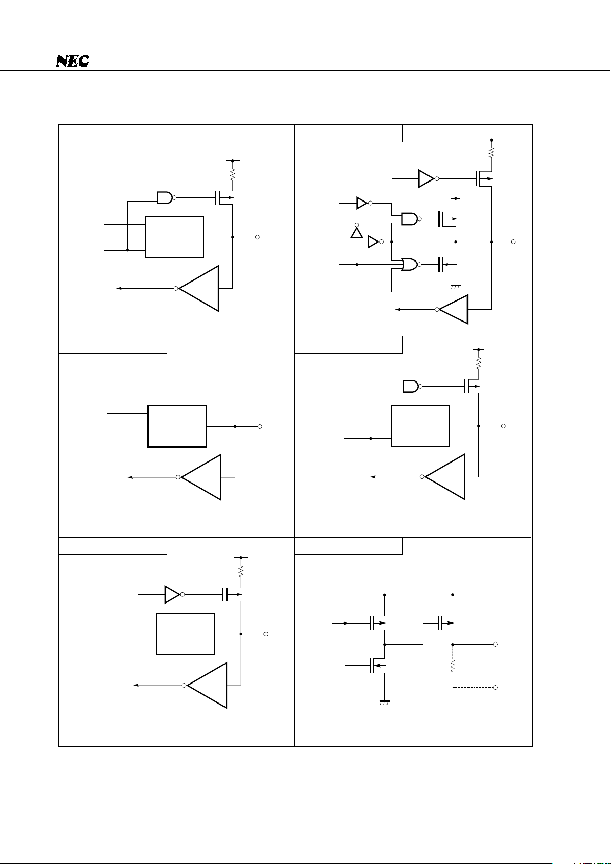
1.3 PIN INPUT/OUTPUT CIRCUITS (1/4)
Type A
CMOS input buffer
Schmitt trigger input with hysteresis
Push-pull output which can be set to high-impedance output
(off for both P-ch and N-ch)
I/O circuit consisting of a push-pull output
of type D and an input buffer of type A
P.U.R.: Pull-Up Resistor
Type B Type E
Type B - C
Type D
IN
IN
IN
P-ch
P.U.R.
enable
P.U.R.
V
DD
V
DD
P-ch
N-ch
OUT
Data
Output
disable
IN/OUT
Data
Output
disable
Type D
Schmitt trigger input with hysteresis
P.U.R.: Pull-Up Resistor
P.U.R.
V
DD
Output
disable
P-ch
IN/OUT
Data
Output
disable
Type D
Type E - B
Type A
Type A
V
DD
P-ch
N-ch
12
µ
PD75238
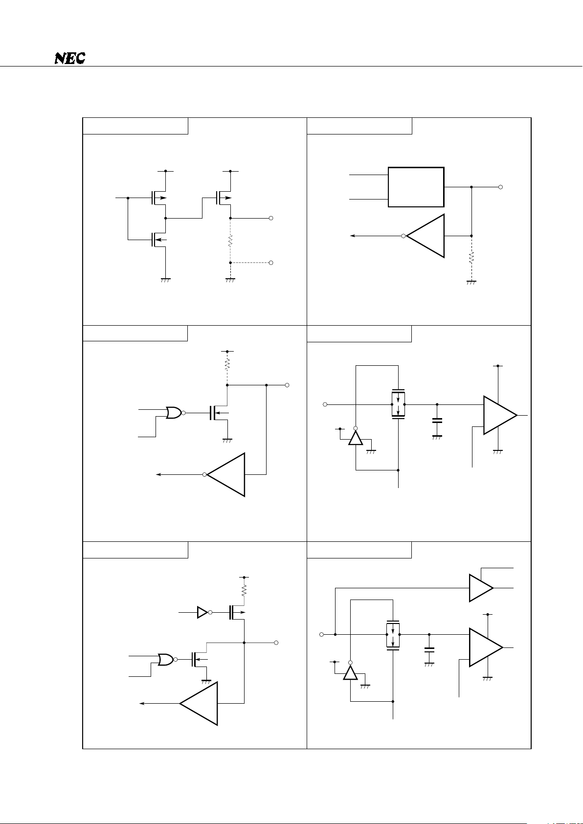
1.3 PIN INPUT/OUTPUT CIRCUITS (2/4)
Type E - C
I/O circuit consisting of a push-pull output of type D
and a Schmitt-triggered input of type B
P.U.R.: Pull-Up Resistor
Type F
Type F - A
Type F - B
P.U.R.
V
DD
P.U.R.
enable
P-ch
IN/OUT
Data
Output
disable
Type D
IN/OUT
Data
Output
disable
Type D
P.U.R.: Pull-Up Resistor
P.U.R.
V
DD
P.U.R.
enable
P-ch
IN/OUT
Data
Output
disable
Type D
P.U.R.: Pull-Up Resistor
V
DD
P-ch
N-ch
IN/OUT
V
DD
P-ch
P.U.R.
P.U.R.
enable
Output
disable
(P-ch)
Data
Output
disable
Output
disable
(N-ch)
Type F - C
P.U.R.: Pull-Up Resistor
P.U.R.
V
DD
P.U.R.
enable
P-ch
IN/OUT
Data
Output
disable
Type D
Type B
Type A
Type B
Type B
Type B
Type I - C
Data
V
DD
V
DD
P-ch P-ch
N-ch
OUT
V
LOAD
P.D.R.
(Mask option)
P.D.R.: Pull-Down Resistor
13
µ
PD75238
1.3 PIN INPUT/OUTPUT CIRCUITS (3/4)
Type V
Type M - C
Type Y
Type Y - A
P.D.R.: Pull-Down Resistor
P.U.R.: Pull-Up Resistor
P.D.R.
(Mask option)
IN/OUT
Data
Output
disable
Type D
N-ch
P.U.R.
Data
Output
disable
P.U.R.
enable
V
DD
P-ch
IN/OUT
AV
DD
AV
DD
P-ch
AV
SS
N-ch
Sampl-
ing C
AV
SS
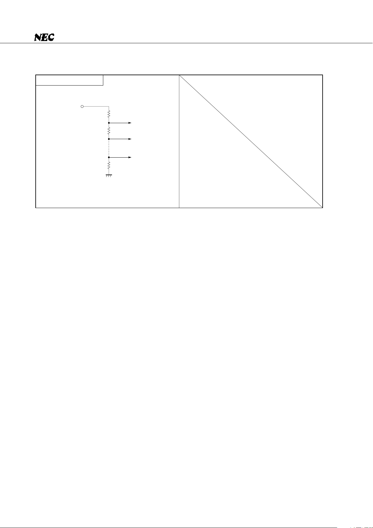
Reference voltage
(from voltage tap of
serial resistor string)
IN
AV
DD
AV
SS
Sampl-
ing C
AV
DD
AV
SS
IN
Reference voltage
(from voltage tap of
serial resistor string)
Type A
Type M
P.U.R.: Pull-Up Resistor
N-ch
IN/OUT
Data
V
DD
Output
disable
P.U.R.
(Mask option)
Middle-voltage input buffer
Type I - F
AV
SS
–
P-ch
N-ch
+
–
+
AV
SS
Type B
Data
V
DD
V
DD
P-ch P-ch
N-ch
OUT
V
LOAD
P.D.R.
(Mask option)
P.D.R.: Pull-Down Resistor
14
µ
PD75238
1.3 PIN INPUT/OUTPUT CIRCUITS (4/4)
Type Z
AV
SS

15
µ
PD75238
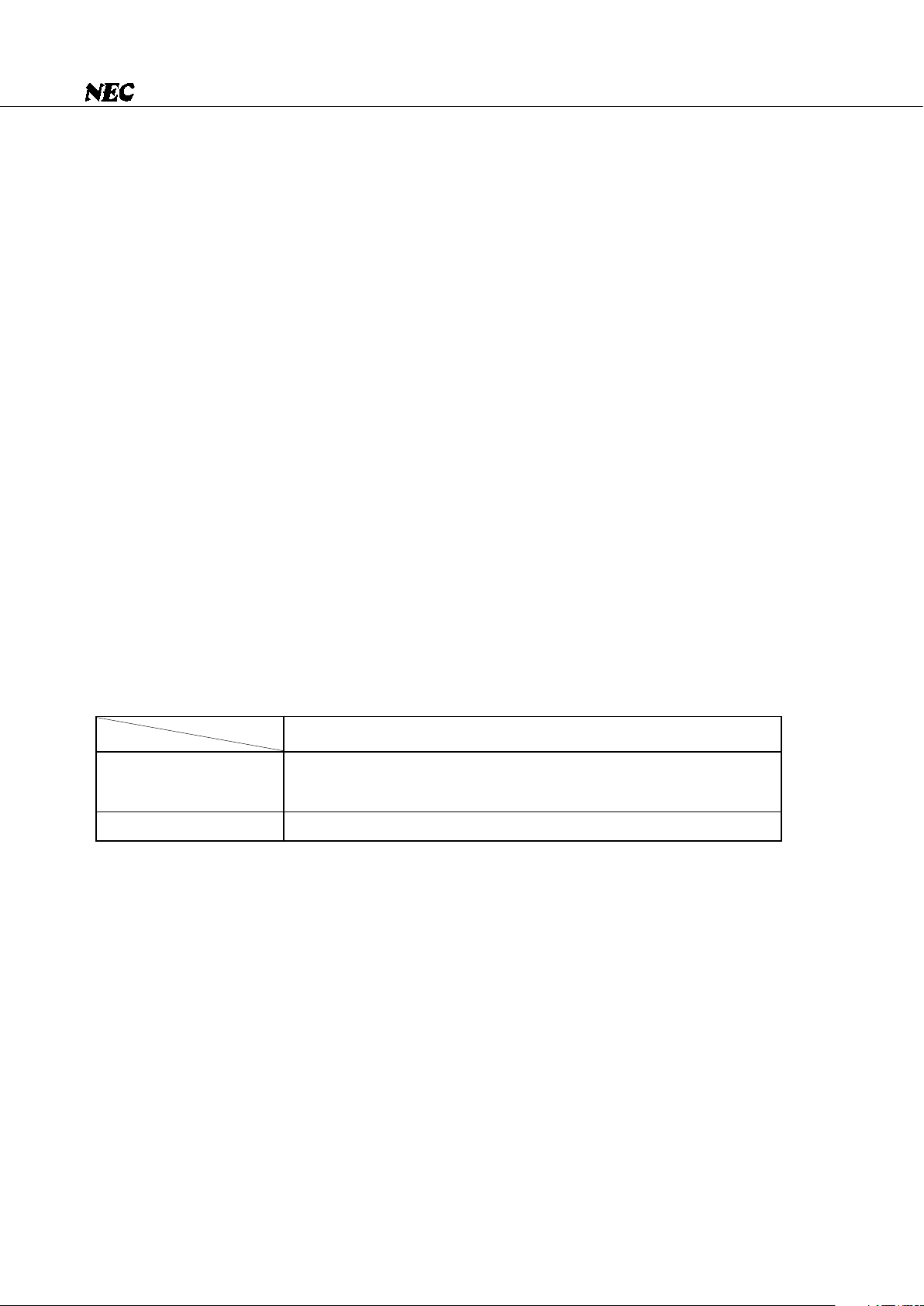
1.4 CONNECTION OF UNUSED µPD75238 PINS
To be connected to VSS
To be connected to VSS or VDD
To be connected to VSS
Input state : To be connected to VSS or VDD
Output state: To be left open
To be connected to VSS
To be left open
To be connected to VSS
To be connected to VDD
To be connected to VSS
To be connected to VSS or VDD
To be left open
To be connected to VSS
Pin name Recommended connection
P00/INT4
P01/SCK0
P02/SO0/SB0
P03/SI1/SB1
P10/INT0-P12/INT2
P13/TI0
P20/PTO0
P21
P22/PCL
P23/BUZ
P30-P33
P40-P43
P50-P53
P60-P63
P70-P73
P80/PPO
P81/SCK1
P82/SO1
P83/SI1
P90/AN4-P93/AN7
P100/S16-P103/S19
P110/S20-P113/S23
P120-P123
P130-P133
P140-P143
P150-P153
AN0-AN3
AVREF
AVDD
AVSS
XT1
XT2
VLOAD
16
µ
PD75238
2. ARCHITECTURE AND MEMORY MAP OF THE µPD75238
The µPD75238 has three architectural features:
(a) Data memory bank configuration
(b) General register bank configuration
(c) Memory-mapped I/O
Each of these features is explained below.
2.1 DATA MEMORY BANK CONFIGURATION AND ADDRESSING MODES
As shown in Fig. 2-1, the data memory space of the
µ
PD75238 contains a static RAM (928 words × 4 bits)
at addresses 000H to 19FH and 200H to 3FFH, a display data memory (96 words × 4 bits) at addresses 1A0H
to 1FFH, and peripheral hardware (such as I/O ports and timers) at addresses F80H to FFFH. To address a 12bit address in this data memory space, the
µ
PD75238 uses such a memory bank configuration that the loworder eight bits are specified with an instruction directly or indirectly, and the high-order four bits are used
to specify a memory bank (MB).
To specify a memory bank (MB), a memory bank enable flag (MBE) and memory bank select register (MBS)
are contained, allowing the addressing indicated in Fig. 2-1 and Table 2-1. (The MBS is a register used to select
a memory bank, and can be set to 0, 1, 2, 3, or 15. The MBE is a flag used to determine whether a memory
bank selected using the MBS register is to be enabled. The MBE is automatically saved or restored at the time
of interrupt processing or subroutine processing, so that it can be freely set in interrupt processing and
subroutine processing.)
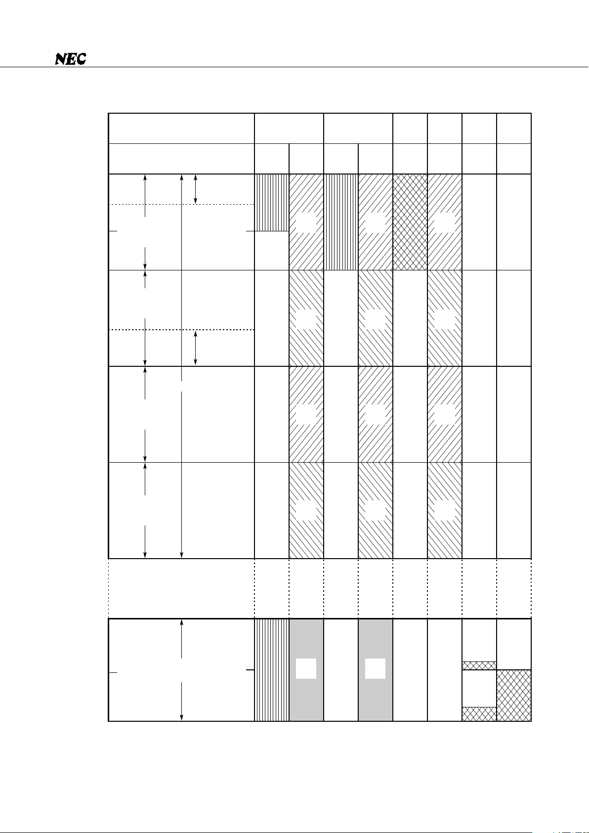
In addressing data memory space, the MBE is usually set to 1 (MBE = 1), and the static RAM in the memory
bank specified by the MBS is operated. However, the MBE = 0 mode or the MBE = 1 mode can be selected
for each step of program processing for more efficient programming.
• Interrupt processing
• Processing that repeats internal hardware and static RAM operations
• Subroutine processing
• Usual program processing
MBE = 0 mode
MBE = 1 mode
Applicable program processing
17
µ
PD75238
Fig. 2-1 Data Memory Organization and Addressing Range of Each Addressing Mode
Remark — : Don’t care
FFFH
FC0H
F80H
3FFH
2FFH
300H
1FFH
200H
0FFH
100H
01FH
020H
000H
Addressing mode
mem
mem.bit
@HL
@H + mem.bit
@DE
@DL
Stack
address-
ing
fmem.bit
pmem.
@L
Memory bank enable flag
MBE
= 0
MBE
= 1
MBE
= 0
MBE
= 1
––– –
Data area
Static RAM
(memory bank 0)
Data area
Static RAM
(memory bank 1)
Data area
Static RAM
(memory bank 2)
Data area
Static RAM
(memory bank 3)
Stack area
Not contained
Peripheral hardware area
(memory bank 15)
MBS
= 0
MBS
= 0
SBS
= 0
MBS
= 1
MBS
= 1
SBS
= 1
MBS
= 2
MBS
= 2
SBS
= 2
MBS
= 3
MBS
= 3
SBS
= 3
MBS
= 15
MBS
= 15
General
resister
area
19FH
1A0H
Display data
memory area
07FH

18
µ
PD75238
Table 2-1 Addressing Modes
As summarized in Table 2-1, the µPD75238 allows both direct and indirect addressing in data memory
manipulation for 1-bit data, 4-bit data, and 8-bit data, so that very efficient and simple programming can be
performed.
Bit specified by bit at the address specified by MB and mem. In this case:
When MBE = 0 and mem = 00H-7FH, MB = 0
When MBE = 0 and mem = 80H-FFH, MB = 15
When MBE = 1, MB = MBS
Address specified by MB and mem. In this case:
When MBE = 0 and mem = 00H-7FH, MB = 0
When MBE = 0 and mem = 80H-FFH, MB = 15
When MBE = 1, MB = MBS
Address specified by MB and mem (mem: even address). In this case:
When MBE = 0 and mem = 00H-7FH, MB = 0
When MBE = 0 and mem = 80H-FFH, MB = 15
When MBE = 1, MB = MBS
Address specified by MB and HL. In this case, MB = MBE• MBS
Address specified by MB and HL. In this case, MB = MBE• MBS.
HL+ automatically increments the L register after addressing.
HL- automatically decrements the L register after addressing.
Address specified by DE in memory bank 0
Address specified by DL in memory bank 0
Address specified by MB and HL.
In this case, MB = MBE• MBS. Bit 0 of the L resister is ignored.
Bit specified by bit at the address specified by fmem. In this case:
fmem = FB0H-FBFH (interrupt-related hardware)
fmem = FF0H-FFFH (I/O port)
Bit specified by the low-order 2 bits of the L register at the address specified
by the high-order 10 bits of pmem and the high-order 2 bits of the L register.
In this case, pmem = FC0H-FFFH
Bit specified by bit at the address specified by MB, H, and the low-order 4 bits
of mem.
In this case, MB = MBE• MBS
Address specified by SP in memory bank 0, 1, 2, and 3 selected by SBS
1-bit direct addressing
4-bit direct addressing
8-bit direct addressing
4-bit register indirect
addressing
8-bit register indirect
addressing
Bit manipulation
addressing
Stack addressing
mem.bit
mem
@HL
@HL+
@HL–
@DE
@DL
@HL
fmem.bit
pmem.@L
@H+mem.bit
–
Representation
format
Specified addressAddressing mode

19
µ
PD75238
2.2 GENERAL REGISTER BANK CONFIGURATION
The
µ
PD75238 contains four register banks, each consisting of eight general registers: X, A, B, C, D, E, H,
and L. These registers are mapped to addresses 00H to 1FH in memory bank 0 of the data memory. (See Fig.
2-2.) To specify a general register bank, a register bank enable flag (RBE) and a register bank select register
(RBS) are contained. The RBS is a register used to select a register bank, and the RBE is a flag used to determine
whether a register bank selected using the RBS is to be enabled. The register bank (RB) enabled at instruction
execution is determined as RB = RBE• RBS
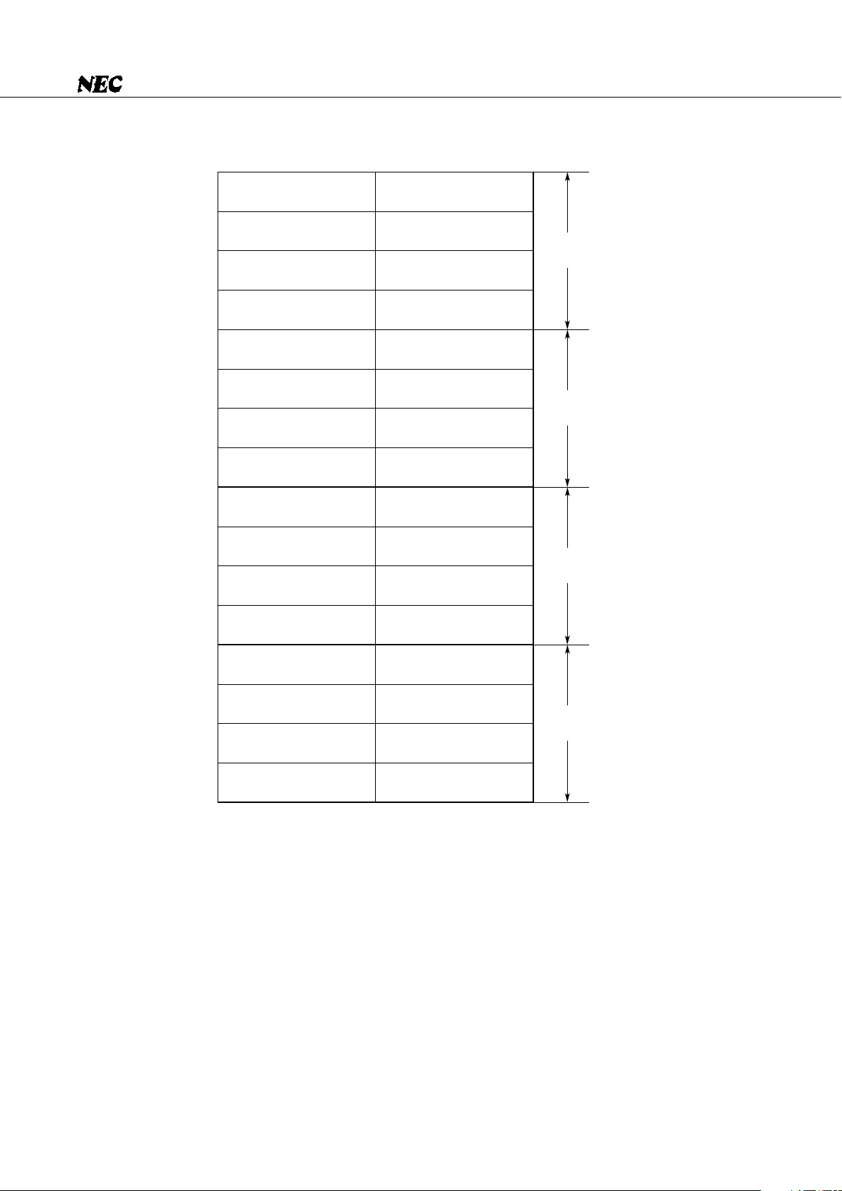
As indicated in Table 2-2, the
µ
PD75238 enables the user to create programs in a very efficient manner by
selecting a register bank from the four register banks, depending on whether the processing is normal
processing or interrupt processing. (The RBE is automatically saved and set at the time of interrupt processing,
and is automatically restored upon completion of interrupt processing.)
Table 2-2 Recommended Use of Register Banks with Normal Routines and Interrupt Routines
The general registers allow transfers, comparisons, arithmetic/logical operations, and increments and
decrements not only on a 4-bit basis, but also on an 8-bit basis with the XA, HL, DE, and BC register pairs.
In this case, the register pairs of the register bank that has the inverted value of bit 0 of a register bank specified
by RBE• RBS can be specified as XA’, HL’, DE’, and BC’, thus providing eight 8-bit registers. (See Fig. 2-3.)
Normal processing
Single interrupt processing
Dual interrupt processing
Multiple (triple or more) interrupt processing
Use register banks 2 and 3 with RBE = 1.
Use register bank 0 with RBE = 0.
Use register bank 1 with RBE = 1.
(In this case, the RBS needs to be saved and restored.)
Save and restore the registers with PUSH or POP.
20
µ
PD75238
Fig. 2-2 General Register Configuration (4-Bit Processing)
X
H
D
B
X
H
D
B
X
H
D
B
X
H
D
B
01H
03H
05H
07H
09H
0BH
0DH
0FH
11H
13H
15H
17H
19H
1BH
1DH
1FH
A
L
E
C
A
L
E
C
A
L
E
C
A
L
E
C
00H
02H
04H
06H
08H
0AH
0CH
0EH
10H
12H
14H
16H
18H
1AH
1CH
1EH
Register bank 0
(RBE
•
RBS = 0)
Register bank 1
(RBE
•
RBS = 1)
Register bank 2
(RBE
•
RBS = 2)
Register bank 3
(RBE
•
RBS = 3)
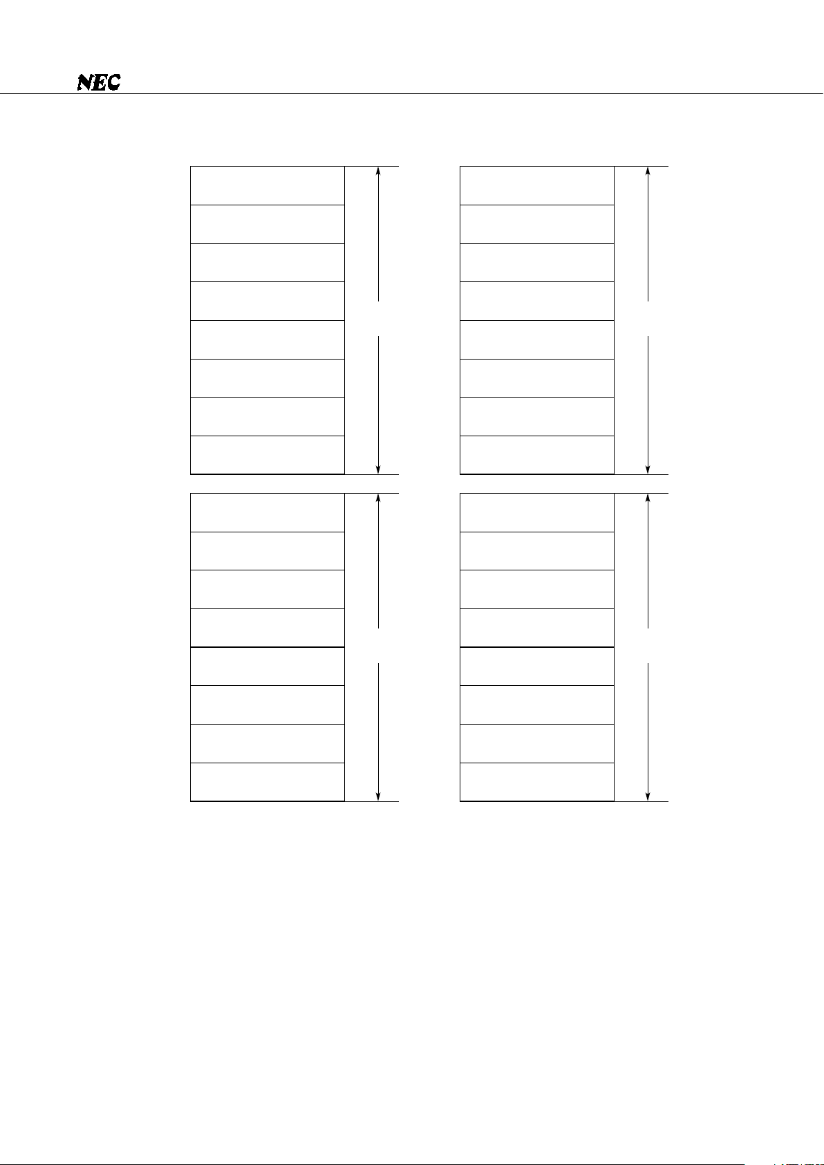
21
µ
PD75238
Fig. 2-3 General Register Configuration (8-Bit Processing)
XA
HL
DE
BC
XA’
HL’
DE’
BC’
00H
02H
04H
06H
08H
0AH
0CH
0EH
When RBE•RBS
= 0
XA’
HL’
DE’
BC’
XA
HL
DE
BC
00H
02H
04H
06H
08H
0AH
0CH
0EH
When RBE•RBS
= 1
XA
HL
DE
BC
XA’
HL’
DE’
BC’
10H
12H
14H
16H
18H
1AH
1CH
1EH
When RBE•RBS
= 2
XA’
HL’
DE’
BC’
XA
HL
DE
BC
10H
12H
14H
16H
18H
1AH
1CH
1EH
When RBE•RBS
= 3

22
µ
PD75238
2.3 MEMORY-MAPPED I/O
The
µ
PD75238 employs memory-mapped I/O, which maps peripheral hardware such as timers and I/O ports
to addresses F80H to FFFH in the data memory space as shown in Fig. 2-1. This means that there is no particular
instruction to control peripheral hardware, but all peripheral hardware is controlled using memory manipulation instructions. (Some mnemonics for hardware control are available to make programs readable.)
To manipulate peripheral hardware, the addressing modes listed in Table 2-3 can be used.
The display data memory, key scan registers, and port H mapped to addresses 1A0H to 1FFH are to be
manipulated by specifying memory bank 1.
Table 2-3 Addressing Modes Applicable to Peripheral Hardware Mapped to Addresses F80H to FFFH
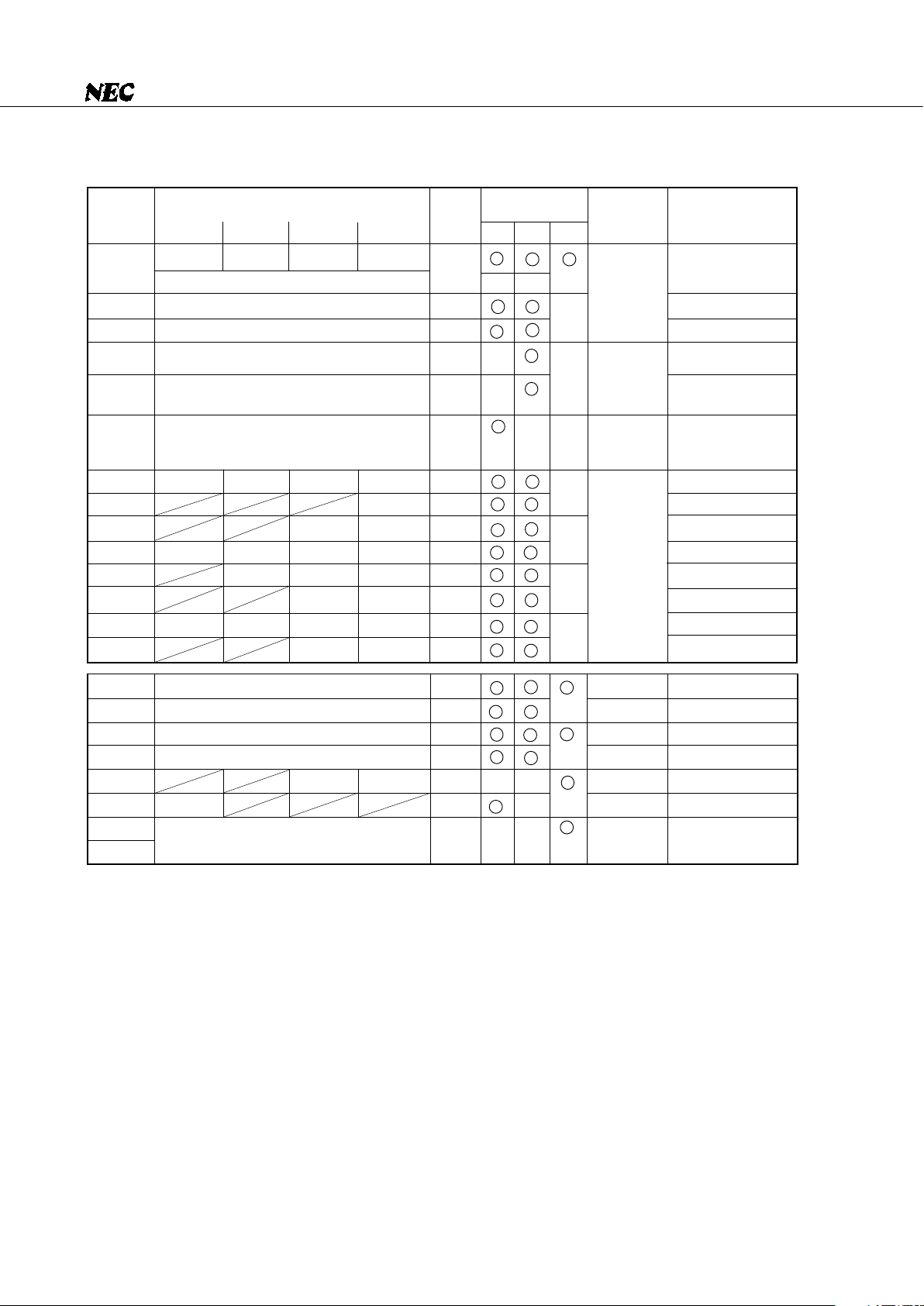
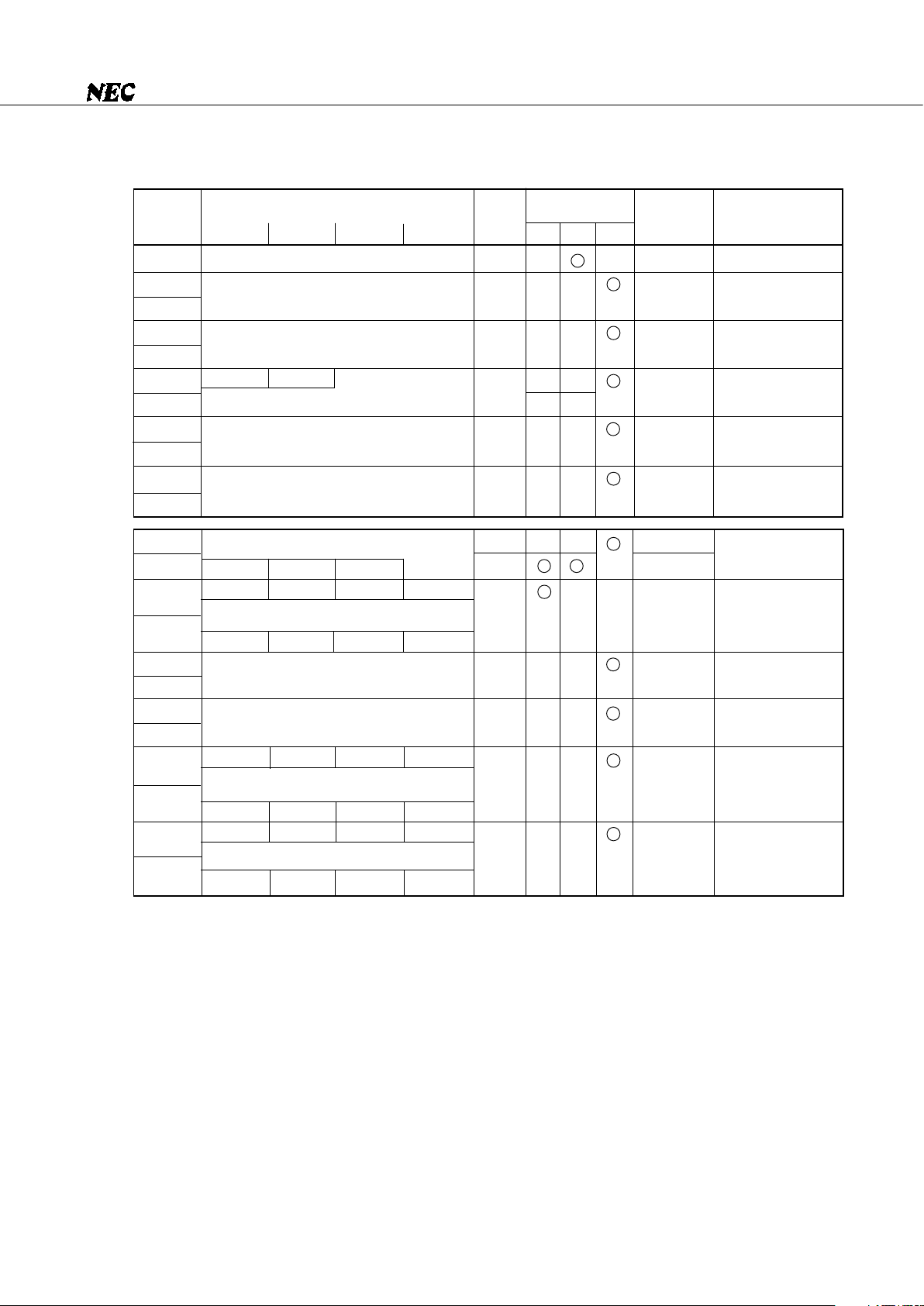
Table 2-4 summarizes the I/O map of the µPD75238.
The items in Table 2-4 have the following meanings:
• Symbol: Name representing the address of incorporated hardware, which can be coded in the operand
field of an instruction
• R/W : Indicates whether the hardware allows read/write operation.
R/W: Both read and write operations possible
R : Read only
W : Write only
• Number of manipulatable bits:
Indicates the number of bits that can be processed in hardware manipulation
• Bit manipulation addressing:
Bit manipulation addressing applicable in hardware bit manipulation
Bit manipulation
4-bit manipulation
8-bit manipulation
Direct addressing mode specifying mem.bit with MBE = 0 or
(MBE = 1, MBS = 15)
Direct addressing mode specifying fmem.bit regardless of MBE
and MBS setting
Indirect addressing mode specifying pmem.@L regardless of
MBE and MBS setting
Direct addressing mode specifying mem with MBE = 0 or (MBE
= 1, MBS = 15)
Register indirect addressing mode specifying @HL with (MBE
= 1, MBS = 15)
Direct addressing mode specifying mem (even address) with
MBE = 0 or (MBE = 1, MBS = 15)
Register indirect addressing mode specifying @HL (with the L
register containing an even number) with (MBE = 1, MBS = 15)
All hardware allowing bit
manipulation
IST0, IST1, MBE, RBE,
IE×××, IRQ×××, PORTn.0-3
PORTn.
All hardware allowing 4-bit
manipulation
All hardware allowing 8-bit
manipulation addressing
Applicable addressing mode
Applicable hardware
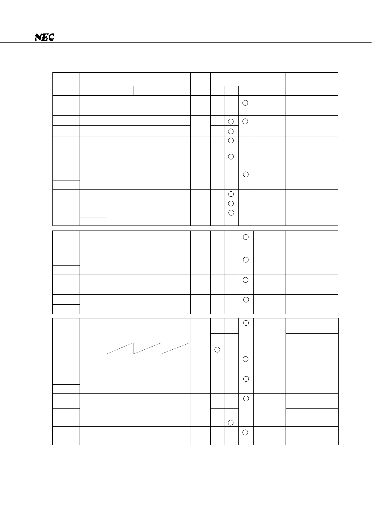
23
µ
PD75238
mem.bit
mem.bit
mem.bit
1 bit 4 bits 8 bits
b3 b2 b1 b0
Hardware name (symbol)
Remarks
R/W
Bit manipulation addressing
Address
F80H
F82H
F83H
F84H
F85H
F86H
F88H
F89H
F8AH
F90H
F94H
F96H
F98H
FA0H
FA2H
FA4H
FA6H
FA8H
FABH
FACH
Stack pointer (SP)
Resister bank select register (RBS)
Memory bank select register (MBS)
Stack bank select register (SBS)
Basic interval timer mode register (BTM)
Basic interval timer (BT)
Display mode register (DSPM)
Dimmer select register (DIMS)
KSF Digit select register (DIGS)
Timer pulse generator mode register (TPGM)
Timer pulse generator modulo register L
(MODL)
Timer pulse generator modulo register H (MODH)
Clock mode register (WM)
Timer/event counter 0 mode register (TM0)
TOE0
Timer/event counter 0 count register (T0)
Timer/event counter 0 modulo register (TMOD0)
Event counter mode register (TM1)
Gate control register (GATEC)
Count register (T1)
R/W – –
R
Note 1
–
–
R/W – –
W ∆ –
R––
W– –
W– –
R/W ∆ –
W ∆∆
R/W – –
R/W – –
W––
W∆–
––
W––
R––
W––
W∆–
––
W– –
R–
Number of manipulatable bits
Bit 0 is always set to
0.
Bits 2 and 3 are
always set to 0.
Only bit 3 allows bit
manipulation.
Only bit 3 allows a
bit test.
Only bit 3 allows bit
manipulation.
Only bit 3 allows bit
manipulation.
Only bit 3 allows bit
manipulation.
Note 2
★
Table 2-4 µPD75238 I/O Map (1/4)
Notes 1. For the SEL instruction, these registers are both readable and writable.
2. Can be operated separately as the RBS and MBS during 4-bit manipulation.
Can also be operated as the BS during 8-bit manipulation.
–
24
µ
PD75238
Table 2-4 µPD75238 I/O Map (2/4)
IST1 IST0 MBE RBE
Program status word (PSW)
Interrupt priority select register (IPS)
Processor clock control register (PCC)
INT0 mode register (IM0)
INT1 mode register (IM1)
System clock control register (SCC)
IE4 IRQ4 IEBT IRQBT
EOT
IEW IRQW
IEKS IRQKS IETPG IRQTPG
IRQT1 IET0 IRQT0
IECSI0 IRQCSI0
IE1 IRQ1 IE0 IRQ0
IE2 IRQ2
Bit sequential buffer 0 (BSB0)
Bit sequential buffer 1 (BSB1)
Bit sequential buffer 2 (BSB2)
Bit sequential buffer 3 (BSB3)
CSIM11 CSIM10
CSIE1
Serial I/O shift register 1 (SIO1)
R/W
––
W–
W
W– –
W–
W––
R/W –
R/W
R/W –
R/W
R/W –
R/W
R/W –
R/W
R/W
R/W
R/W
R/W
W––
W–
R/W – –
1 bit 4 bits 8 bits
Number of manipulatable bits
b3 b2 b1 b0
Hardware name (symbol)
Remarks
R/W
Bit manipulation addressing
Address
Bit 2 is always set to
0.
Bits 1, 2, and 3 are
always set to 0.
Only bits 0 and 3
allow bit manipula-
tion.
★
★
★
FB0H
FB2H
FB3H
FB4H
FB5H
FB7H
FB8H
FB9H
FBAH
FBBH
FBCH
FBDH
FBEH
FBFH
FC0H
FC1H
FC2H
FC3H
FC8H
FC9H
FCCH
fmem.bit
fmem.bit
25
µ
PD75238
Table 2-4 µPD75238 I/O Map (3/4)
W– –
W––
W––
R/W ∆ –
––
R––
W––
W––
R/W
R/W – –
R/W – –
W––
W––
W––
1 bit 4 bits 8 bits
Number of manipulatable bits
b3 b2 b1 b0
Hardware name (symbol)
Remarks
R/W
Bit manipulation addressing
Address
ADM is write only
during 8-bit manipulation.
CSIM0 is write only
during 8-bit manipulation.
mem.bit
mem.bit
Clock output mode register (CLOM)
Static mode register B (STATB)
Static mode register A (STATA)
SOC EOC
A/D conversion mode register (ADM)
SA register (SA)
Pull-up resistor specification register group
A (POGA)
Serial operation mode register (CSIM0)
CSIE0 COI WUP
CMDD RELD CMDT RELT
SBI control register (SBIC)
BSYE ACKD ACKE ACKT
Serial I/O shift register 0 (SIO0)
Slave address register (SVA)
PM33 PM32 PM31 PM30
Port mode register group A (PMGA)
PM63 PM62 PM61 PM60
– PM2 – –
Port mode register group B (PMGB)
PM7 – PM5 PM4
★
FD0H
FD4H
FD6H
FD8H
FDAH
FDCH
FE0H
FE2H
FE4H
FE6H
FE8H
FECH
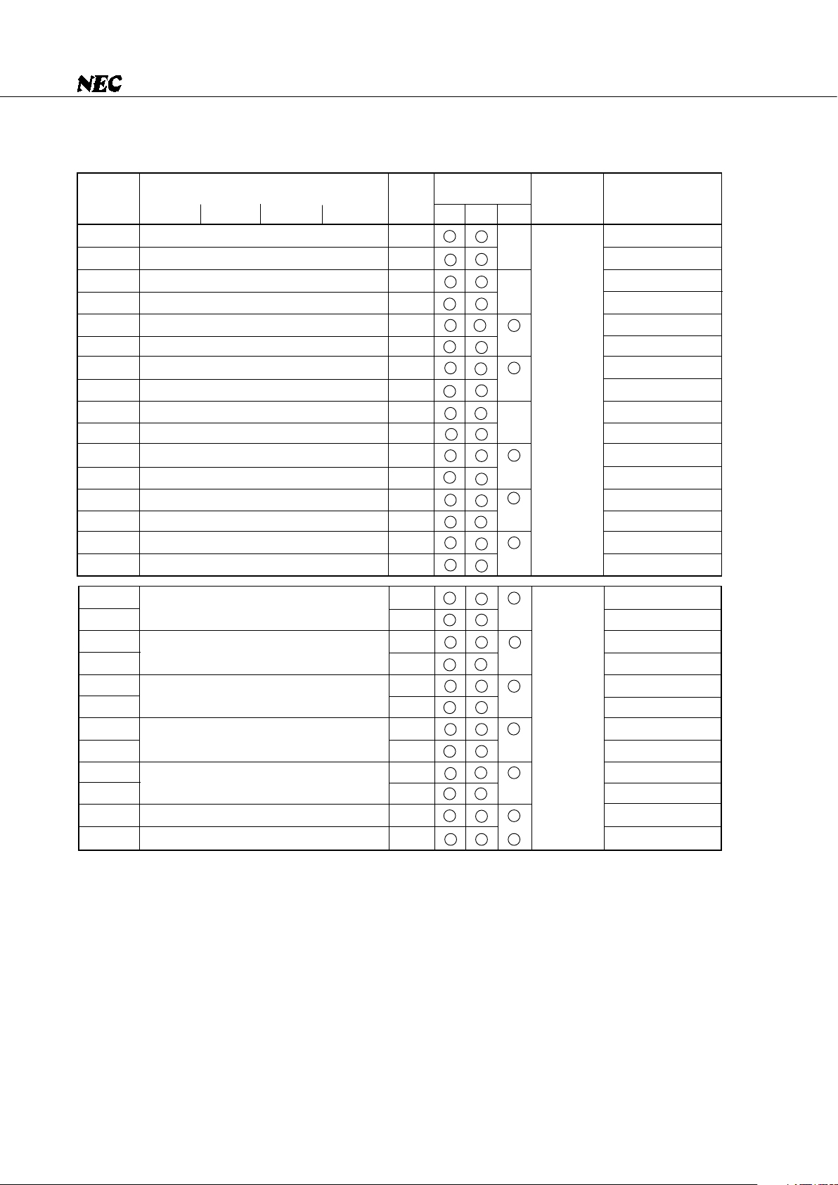
26
µ
PD75238
Table 2-4 µPD75238 I/O Map (4/4)
Port 0 (PORT0)
Port 1 (PORT1)
Port 2 (PORT2)
Port 3 (PORT3)
Port 4 (PORT4)
Port 5 (PORT5)
Port 6 (PORT6)
Port 7 (PORT7)
Port 8 (PORT8)
Port 9 (PORT9)
Port 10 (PORT10)
Port 11 (PORT11)
Port 12 (PORT12)
Port 13 (PORT13)
Port 14 (PORT14)
Port 15 (PORT15)
Display data memory: S16-S23 (n = 0 to 15)
Key scan register (KS2)
Display data memory: S0-S7 (n = 0 to 15)
Display data memory: S8-S15 (n = 0 to 15)
Key scan register (KS0)
Key scan register (KS1)
Port H (PORTH)
1 bit 4 bits 8 bits
Number of manipulatable bits
b3 b2 b1 b0
Hardware name (symbol)
Remarks
R/W
Bit manipulation addressing
Address
fmem.bit
pmem.@L
mem.bit
FF0H
FF1H
FF2H
FF3H
FF4H
FF5H
FF6H
FF7H
FF8H
FF9H
FFAH
FFBH
FFCH
FFDH
FFEH
FFFH
1A0H+4n
1A1H+4n
1BEH
1BFH
1C0H+4n
1C1H+4n
1C2H+4n
1C3H+4n
1FCH
1FDH
1FEH
1FFH
R–
R
R/W –
R/W
R/W
R/W
R/W
R/W
R–
R
W
W
W
W
W
W
R/W
R/W
R/W
R/W
R/W
R/W
R/W
R/W
R/W
R/W
R/W
R/W

27
µ
PD75238
3. INTERNAL CPU FUNCTIONS
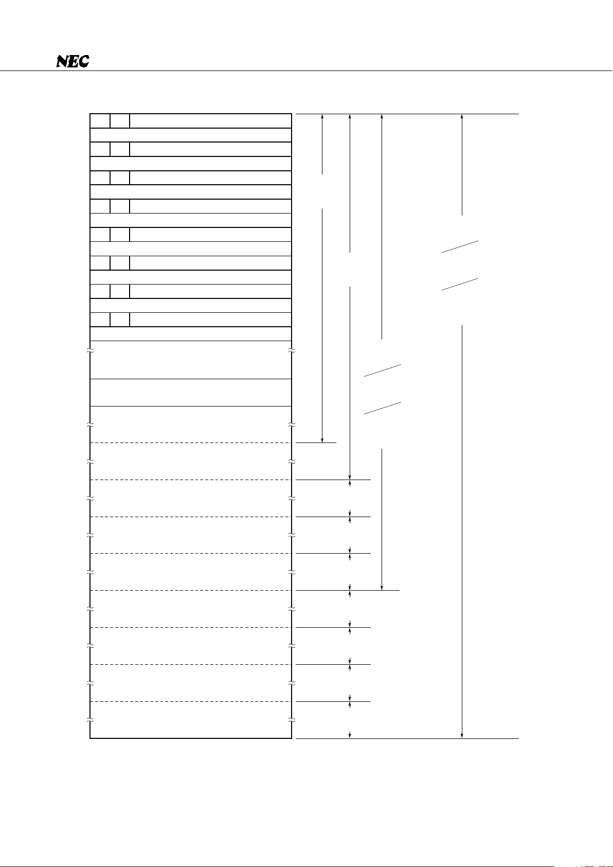
3.1 PROGRAM COUNTER (PC): 15 BITS
The program counter is a 15-bit binary counter for holding program memory address information.
Fig. 3-1 Program Counter Format
Note that the reset start address must be set within a space of 16K bytes (0000H to 3FFFH). This is because
a RESET input sets the low-order six bits of program memory address 0000H in PC13 to PC8, and the contents
of address 0001H in PC7 to PC0 for initialization.
3.2 PROGRAM MEMORY (ROM): 32640 WORDS × 8 BITS
The program memory is a mask-programmable ROM with a configuration of 32640 words × 8 bits for storing
programs, table data, and so forth.
Program memory is addressed by the program counter. Table data can be referenced using the table
reference instruction (MOVT).
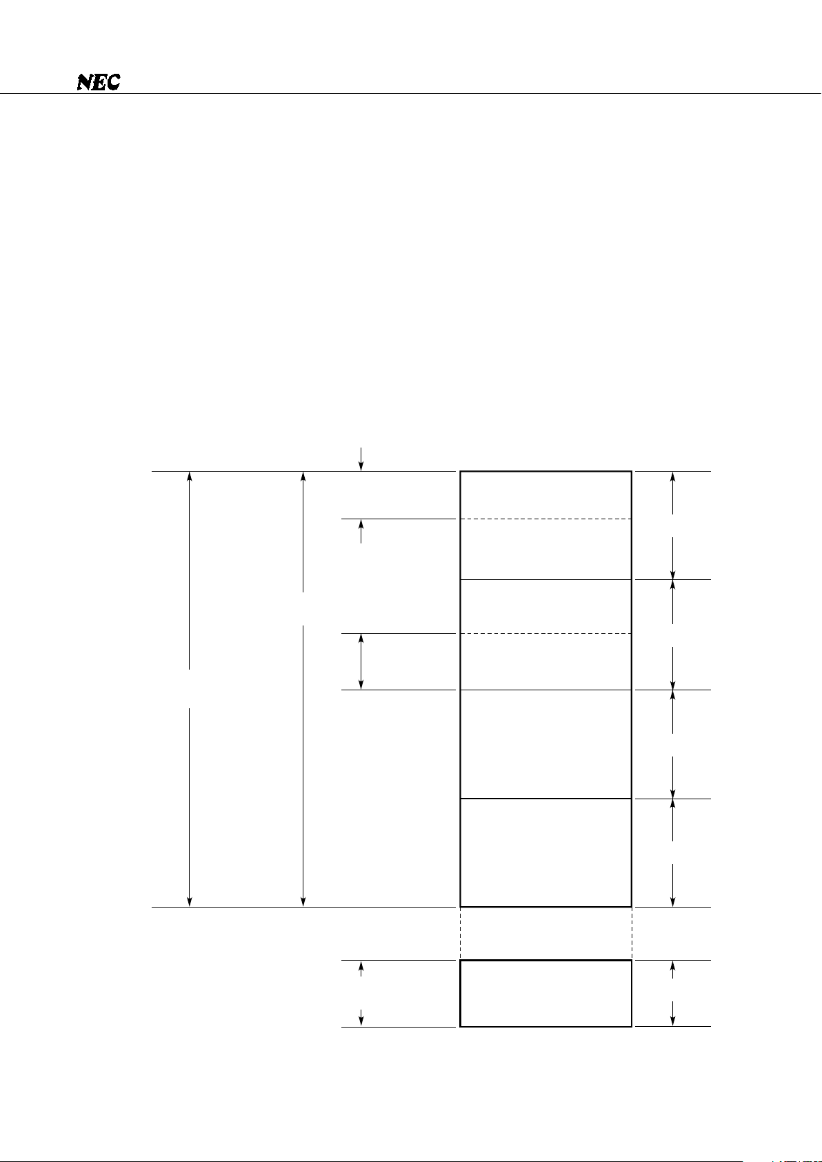
Fig. 3-2 shows the allowable branch address ranges for the branch instructions and subroutine call
instructions. The whole-space branch instruction (BRA !addr1) and the whole-space call instruction (CALLA
!addr1) allow a direct branch throughout the whole space 0000H to 7F7FH. The relative branch instruction
(BR $addr) allows a branch to addresses (PC - 15 to PC - 1 and PC + 2 to PC + 16) regardless of block boundaries.
The program memory is located at addresses 0000H to 7F7FH containing the following specially assigned
addresses. (All areas excluding 0000H and 0001H can be used as normal program memory.)
• 0000H to 0001H
Vector table for holding the RBE and MBE setting values and program start address at the time of a RESET
input. A reset start can be performed at an arbitrary address within a 16K-byte space (0000H to 3FFFH).
• 0002H to 000FH
Vector address table for holding the RBE and MBE setting values and program start address at the time
of each vectored interrupt occurrence. Interrupt processing can be started at an arbitrary address within
a 16K-byte space (0000H to 3FFFH).
• 0020H to 007FH
Table area referenced by the GETI instruction
Note
Note The GETI instruction can represent an arbitrary 2-byte or 3-byte instruction or two 1-byte instructions
in 1 byte, thus reducing the number of program bytes. (See Section 8.1.)
PC14 PC13 PC12 PC11 PC10 PC9 PC8 PC7 PC6 PC5 PC4 PC3 PC2 PC1 PC0
28
µ
PD75238
Fig. 3-2 Program Memory Map
Caution The start address of an interrupt vector shown above consists of 14 bits. So, the start address
must be set within a 16K-byte space (0000H to 3FFFH).
Remark In addition to the above, the BR PCDE and BR PCXA instructions can cause a branch to an address
with only the low-order 8 bits of the PC changed.
Internal reset start address
BRCB !caddr
instruction
branch address
MBE RBE
Internal reset start address
INTBT/INT4 start address
MBE RBE
INTBT/INT4 start address
MBE RBE
INT0 start address
INT0 start address
MBE RBE
INT1 start address
INT1 start address
MBE RBE
INTSO start address
INTSO start address
MBE RBE
INTT0 start address
INTT0 start address
MBE RBE
INTTPG start address
INTTPG start address
MBE RBE
INTKS start address
INTKS start address
GETI instruction reference table
0000H
0002H
0004H
0006H
0008H
000AH
000CH
000EH
0020H
007FH
0080H
07FFH
0800H
0FFFH
1000H
1FFFH
2000H
2FFFH
3000H
3FFFH
4000H
4FFFH
5000H
5FFFH
6000H
6FFFH
7000H
7F7FH
CALL !addr
instruction
branch address
Branch/call
address specified
in GETI instruction
CALLF !faddr
instruction
entry address
BRCB !caddr
instruction
branch address
BRCB !caddr
instruction
branch address
BRCB !caddr
instruction
branch address
BRCB !caddr
instruction
branch address
BRCB !caddr
instruction
branch address
BRCB !caddr
instruction
branch address
BRCB !caddr
instruction
branch address
BRA !addr
instruction
branch address
CALLA !addr
instruction
branch address
BR $addr1 instruction
relative branch
address (–15 to –1,
+2 to +16)
BR !addr
instruction
branch address
(low-order 8 bits)
(high-order 6 bits)
(high-order 6 bits)
(low-order 8 bits)
(high-order 6 bits)
(low-order 8 bits)
(high-order 6 bits)
(low-order 8 bits)
(high-order 6 bits)
(low-order 8 bits)
(high-order 6 bits)
(low-order 8 bits)
(high-order 6 bits)
(low-order 8 bits)
(high-order 6 bits)
(low-order 8 bits)
29
µ
PD75238
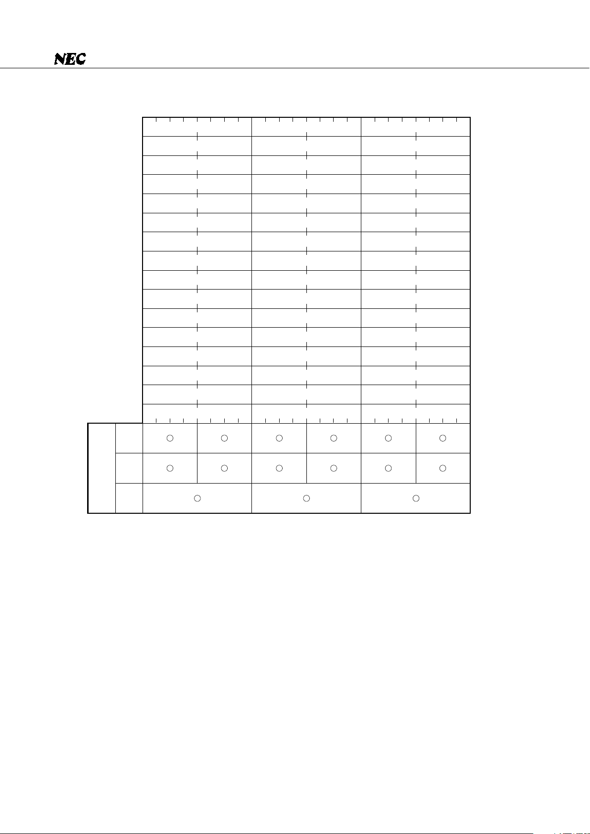
3.3 DATA MEMORY (RAM)
The data memory consists of a static RAM and peripheral hardware.
The static RAM consists of an area of 768 words × 4 bits in memory banks 0, 2, and 3, an area of 160 words
× 4 bits in memory bank 1, and an area of 96 words × 4 bits in memory bank 1, which is used also as display
data memory. The RAM is used for storing processing data, and is also used as stack memory for subroutine
and interrupt execution.
To particular memory addresses, general registers, display data memory, and peripheral hardware (various
registers) are mapped. Data in these areas are manipulated using general register manipulation instructions
and memory manipulation instructions (See Fig. 2-1).
As a stack area, all addresses in memory banks 0, 1, 2, and 3 (000H to 3FFH) can be used.
The data memory has a configuration of 4 bits per address, but allows 8-bit memory manipulation
instructions to be used for 8-bit oriented manipulation, and also allows bit manipulation instructions to be
used for bit-by-bit manipulation. Even addresses are to be specified for 8-bit manipulation instructions.
Fig. 3-4 shows the organization of the display data memory area (1A0H to 1FFH).
Fig. 3-3 Data Memory Map
(32 × 4)
Data memory
000H
01FH
020H
2FFH
300H
3 FFH
F80H
FFFH
256 × 4
256 × 4
128 × 4
0
2
15
Stack
area
General
register
area
Data area
Static RAM
(1024 × 4)
Peripheral
hardware area
Not contained
256 × 4
256 × 4
1
3
0FFH
100H
1FFH
200H
Memory bank
(96 × 4)
1A0H
19FH
Display
data
memory,
etc.
30
µ
PD75238
Fig. 3-4 Display Data Memory Configuration
Remarks 1. KS0, KS1, and KS2 are key scan registers.
2. PORTH is the high-voltage, high-current output port, and is also used for digit output.
1 A 1 H 1 A 0 H 1 C 3 H 1 C 2 H 1 C 1 H 1 C 0 H
1 A 3 H 1 A 2 H 1 C 7 H 1 C 6 H 1 C 5 H 1 C 4 H
1 A 5 H 1 A 4 H 1 C B H 1 C A H 1 C 9 H 1 C 8 H
1 A 7 H 1 A 6 H 1 C F H 1 C E H 1 C D H 1 C C H
1 A 9 H 1 A 8 H 1 D 3 H 1 D 2 H 1 D 1 H 1 D 0 H
1 A B H 1 A A H 1 D 7 H 1 D 6 H 1 D 5 H 1 D 4 H
1 A D H 1 A C H 1 D B H 1 D A H 1 D 9 H 1 D 8 H
1 A F H 1 A E H 1 D F H 1 D E H 1 D D H 1 D C H
1 B 1 H 1 B 0 H 1 E 3 H 1 E 2 H 1 E 1 H 1 E 0 H
1 B 3 H 1 B 2 H 1 E 7 H 1 E 6 H 1 E 5 H 1 E 4 H
1 B 5 H 1 B 4 H 1 E B H 1 E A H 1 E 9 H 1 E 8 H
1 B 7 H 1 B 6 H 1 E F H 1 E E H 1 E D H 1 E C H
1 B 9 H 1 B 8 H 1 F 3 H 1 F 2 H 1 F 1 H 1 F 0 H
1 B B H 1 B A H 1 F 7 H 1 F 6 H 1 F 5 H 1 F 4 H
1 B D H 1 B C H 1 F B H 1 F A H 1 F 9 H 1 F 8 H
1 B F H 1BEH(KS2) 1FFH(PORTH) 1FEH(KS1) 1 F D H 1FCH(KS0)
1
bit
4
bits
8
bits
Number of
manipulatable bits
 Loading...