

DATA SHEET
MOS INTEGRATED CIRCUIT
µ
PD4726
RS-232 LINE DRIVER/RECEIVER
The µPD4726 is a high-voltage silicon gate CMOS line driver/receiver conforming to EIA/TIA-232-E Standards.
It contains a DC/DC converter and can operate with a +5 V single power supply. In addition, it is also provided with
ancillary functions such as a standby function.
This IC is equipped with four driver circuits and seven receiver circuits and can configure a simple RS-232 interface
circuit with only four external capacitors.
FEATURES
Conforms to EIA/TIA-32-E (old RS-232C) Standards
•
+5 V single power supply
•
A standby mode can be set by making the standby pin low to reduce the power dissipation. At this time, the driver
•
outputs go into a high-impedance state.
Two receiver circuits can operate as inverters without a hysteresis width even in the standby mode. The remaining
•
five receiver circuits are fixed to the high level.
ORDERING INFORMATION
Part Number Package Quality Grade
µ
PD4726GS-BAF 36-pin plastic SSOP (300 mil) Standard
Please refer to "Quality grade on NEC Semiconductor Devices" (Document number IEI-1209) published by NEC
Corporation to know the specification of quality grade on the devices and its recommended applications.
Document No. IC-3413 (1st edition)
(O.D.No. IC-8923)
Date Published March 1997 P
Printed in Japan
©
1994
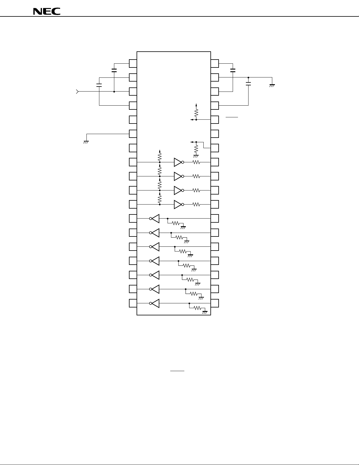
BLOCK DIAGRAM/PIN CONFIGURATION (Top View)
µ
PD4726
+5 V
+10 V
1
V
10
11
12
DD
+
2
C
1
3
V
CC
-
4
C
1
5
N.C.
6
GND
N.C.
7
To internal
circuit
To internal
circuit
8
9
+
C
3
+
C
1
D
IN1
D
IN2
D
IN3
D
IN4
R
OUT1
C
GND
C
V
+
36
4
35
-
34
4
33
SS
32
31
30
29
28
27
26
25
STBY
GND
EN
D
OUT1
D
OUT2
D
OUT3
D
OUT4
R
IN1
+
C
4
+
C
2
−10 V
24
R
23
22
21
20
19
IN2
R
IN3
R
IN4
R
IN5
R
IN6
R
IN7
OUT2
OUT3
OUT4
OUT5
OUT6
OUT7
13
14
15
16
17
18
R
R
R
R
R
R
Notes1. VDD and VSS output internally boosted voltages. Do not connect a load directly to these pins.
2. It is recommended that capacitors having a breakdown voltage of 20 V or higher be used as C
5. Inserting a bypass capacitor of 0.1 to 1
C
µ
F in between VCC and GND is also recommended.
3. Be sure to connect all the GND pins. Especially, make sure that pin 31 is connected; otherwise, the
µ
PD4726 will not operate normally. Be sure to leave the NC pins (pins 5 and 7) open.
4. The pull-up resistors for D
IN1 through DIN4 and STBY and the pull-down resistor for EN are active resistors.
1 through
2
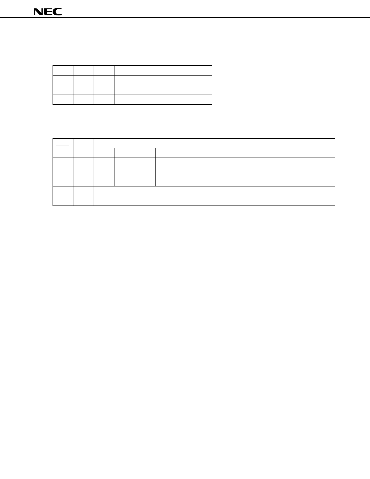
TRUTH TABLE
Drivers
STBY DIN DOUT Remarks
L × Z Standby mode (DC/DC converter stops.)
H L H Space level output
H H L Mark level output
Receivers
µ
PD4726
STBY EN
LL××H H Standby mode 1 (DC/DC converter stops.)
LHL×H H Standby mode 2 (DC/DC converter stops. R6 and R7 operate.)
LHH×LH
H× L H Mark level input
H × H L Space level input
H: high level
L : low level
Z : high impedance
× : H or L
RIN ROUT
R6 - R7 R1 - R5 R6 - R7 R1 - R5
Remarks
3
ABSOLUTE MAXIMUM RATING (Ta = 25 °C)
Parameter Symbol Ratings Unit
Supply voltage VCC −0.5 to +7.0 V
Driver input voltage DIN −0.5 to V CC + 0.5 V
Receiver input voltage RIN −30.0 to +30.0 V
Control input voltage VIN −0.5 to VCC + 0.5 V
(STBY, EN)
Driver output voltage DOUT −25.0 to +25.0
Receiver output voltage ROUT −0.5 to VCC + 0.5 V
Input current (DIN, STBY, EN) IINI ±20.0 mA
Operating ambient temperature Topt. −40 to +85 °C
Storage temperature Tstg. −55 to +150 °C
Permissible package power PT 0.5 W
dissipation
Note 5. Pulse width: 1 ms, duty cycle: 10 % MAX.
Note 5
µ
PD4726
V
RECOMMENDED OPERATING CONDITIONS
Parameter Symbol MIN. TYP. MAX. Unit
Supply voltage (VCHA = L) VCC 4.5 5.0 5.5 V
Input voltage, high (DIN)VIH 2.0 V CC V
Input voltage, low (DIN)VIL 0 0.8 V
Input voltage, high (STBY, EN) VIH 2.4 VCC V
Input voltage, low (STBY, EN) VIL 0 0.8 V
Receiver input voltage RIN −30 +30 V
Operating ambient temperature Topt. −40 +85 °C
External capacitance (nominal value) Note 6 1 4.7
Note 6. Use capacitors whose capacitance fluctuation is within ±50 % including fluctuations due to temperature
µ
and tolerance (effective value: 0.5 to 7.05
F).
Use of capacitors with excellent high-frequency characteristics (such as multilayer ceramic capacitors,
tantalum capacitors, and aluminum electrolytic capacitors for switching power supply) is recommended.
Keep the wiring length between a capacitor and an IC pin as short as possible.
µ
F
4

µ
PD4726
ELECTRICAL SPECIFICATIONS (CHIP)
(Unless otherwise specified, Ta = −40 to +85 °C, C1 through C5 = 1 µF)
Parameter Symbol Conditions MIN. TYP. MAX. Unit
Circuit current ICC1 VCC = +5.0 V, no load, RIN pin open, 12 mA
STBY = H
Circuit current ICC2 VCC = +5.0 V, RL = 3 kΩ (DOUT), 38 mA
DIN = GND, RIN, ROUT pins open,
STBY = H
Circuit current in standby ICC3 VCC = +5.0 V, no load, 9 20
mode (standby mode 1) DIN, RIN pins open, STBY = L, EN = L,
Ta = 25 °C
VCC = +5.0 V, no load, 15
DIN, RIN pins open, STBY = L, EN = L,
Circuit current in standby ICC4 VCC = +5.0 V, no load, 9 20
mode (standby mode 2) DIN, RIN pins open, STBY = L, EN = H,
Ta = 25 °C
VCC = +5.0 V, no load, 15
DIN, RIN pins open, STBY = L, EN = H,
Ta = 25 °C
Input voltage, high VIH STBY, EN pins, 2.4 V
VCC = +4.5 to +5.5 V
Input voltage, low VIL STBY, EN pins, 0.8 V
VCC = +4.5 to +5.5 V
Input current, high IIH STBY pin, VCC = +5.5 V, VI = +5.5 V 1
Input current, low IIL STBY pin, VCC = +5.5 V, VI = 0 V −40
Input current, high IIH EN pin, VCC = +5.5 V, VI = +5.5 V 40
Input current, low IIL EN pin, VCC = +5.5 V, VI = 0 V −1
Input capacitance CIN Driver inputs and receiver inputs, 10 pF
VCC = +5.0 V, vs. GND, f = 1 MHz
µ
A
µ
A
µ
A
µ
A
µ
A
µ
A
µ
A
µ
A
Remark TYP. value is a reference value at Ta = 25 °C.
5

µ
ELECTRICAL SPECIFICATIONS (DRIVERS)
(Unless otherwise specified, Ta = −40 to +85 °C, VCC = +5.0 V ±10 %, C1 through C5 = 1 µF)
Parameter Symbol Conditions MIN. TYP. MAX. Unit
Input voltage, low VIL 0.8 V
Input voltage, high VIH 2.0 V
Input current, low IIL −40
Input current, high IIH 1.0
Output voltage VDO VCC = +5.0 V, RL = ∞, Ta = 25 °C ±9.7 V
VCC = +5.0 V, RL = 3 kΩ, Ta = Topt. ±5.5 V
VCC = +4.5 V, RL = 3 kΩ, Ta = Topt. ±5.0 V
Output short current ISC VCC = +5.0 V, vs. GND ±40 mA
Slew rate SR C L = 10 pF, RL = 3 to 7 kΩ 4.0 30 V/µs
CL = 2 500 pF, RL = 3 to 7 kΩ 4.0 30 V/µs
Propagation delay time
Output resistance R0 VCC = VDD = VSS = 0 V 300 Ω
Standby output transition time tDAZ RL = 3 kΩ, CL = 2500 pF,
Standby output transition time tDZA RL = 3 kΩ, CL = 2500 pF,
Power-ON output transition time tPRA RL = 3 kΩ, CL = 2500 pF,
Note 8
tPHL RL = 3 kΩ, CL = 2 500 pF 2
tPLH
VOUT = ±2 V
Note 9
Note 9
Note 10
410
0.5 1 ms
0.5 1 ms
PD4726
µ
A
µ
A
µ
s
µ
s
Remark TYP. value is a reference value at Ta = 25 °C.
Note 8. Test point
V
CC
D
IN
0 V
+
V
DO
D
OUT
−
V
DO
−3 V
0.8 V
t
PLH
+5 V
+3 V +3 V
+
SR
2.0 V
t
PHL
−3 V
SR
−5 V
−
6

Note 9. Test point
µ
PD4726
V
CC
STBY
0.6 V
0 V
t
DAZ
+
V
DO
D
OUT
−
V
DO
+5 V
High impedance
−5 V
The driver output is undefined during the standby output transition time t
the standby output transition time t
DZA after the standby mode has been released.
Note 10. Test point
5 V
V
CC
0 V
4.5 V
2.4 V
t
DZA
+5 V
−5 V
DZA. Do not perform communication within
t
PRA
+
V
DO
−
DO
High impedance
D
OUT
V
+5 V
−5 V
The driver output is undefined during the power-ON output transition time t
within the power-ON output transition time t
PRA on power application.
PRA. Do not perform communication
7

µ
ELECTRICAL SPECIFICATIONS (RECEIVERS)
(Unless otherwise specified, VCC = 4.5 to 5.5 V, Ta = −40 to +85 °C, C1 through C5 = 1 µF)
Parameter Symbol Conditions MIN. TYP. MAX. Unit
Output voltage, low VOL1 IOUT = 4 mA 0.4 V
(STBY = H)
Output voltage, high V OH1 IOUT = −4 mA VCC − 0.4 V
(STBY = H)
Output voltage, low VOL2 IOUT = 4 mA 0.5 V
(STBY = L)
Output voltage, high V OH2 IOUT = −4 mA VCC − 0.5 V
(STBY = L)
Propagation delay time tPHL RIN → ROUT, CL =150 pF 0.2
(STBY = H) tPLH VCC = +4.5 V,
Propagation delay time tPHL RIN → ROUT (R6, R7), CL =150 pF 0.1
(STBY = L, EN = H) tPLH VCC = +4.5 V,
Propagation delay time tPHA EN → ROUT (R6, R7), CL =150 pF 100 300 ns
(STBY = L) tPAH VCC = +4.5 V,
Input resistance RI 3 5.5 7 kΩ
Open voltage across input pins VIO 0.5 V
Input threshold voltage V IH VCC = +4.5 to +5.5 V 1.7 2.3 2.7 V
(STBY = H)
VIL VCC = +4.5 to +5.5 V 0.7 1.1 1.7 V
VH VCC = +4.5 to +5.5 V 0.5 1.2 1.8 V
(hysteresis width)
Input threshold voltage V IH VCC = +4.5 to +5.5 V, RIN6, RIN7 2.7 1.5 V
(STBY = L, EN = H)
VIL VCC = +4.5 to +5.5 V, RIN6, RIN7 1.5 0.7 V
Standby output transition time tDAH Note 13 0.2 3
Standby output transition time tDHA Note 13 0.3 1 ms
Power-ON output transition time tPRA Note 14 0.5 1 ms
Note 11
Note 11
Note 12
PD4726
µ
s
µ
s
µ
s
Remark TYP. value is a reference value at Ta = 25 °C.
Note 11. Test point
+3 V
R
IN
0 V
0.7 V
−3 V
t
PLH
V
OH
R
OUT
V
OL
2.0 V
8
2.7 V
t
PHL
0.8 V

Note 12. Test point
VCC
µ
PD4726
ROUT
Note 13. Test point
STBY
EN
0 V
VOH
VOL
V
0 V
V
CC
OH
STBY = L
2.4 V
0.6 V
t
DAH
0.8 V
0.6 V
tPAHtPHA
2.4 V
t
DHA
2.0 V
R
OUT
2.0 V
0.8 V
V
OL
The receiver output is undefined during the standby output transition time tDHA. Do not perform communication
within the standby output transition time t
DHA after the standby mode has been released.
Note 14. Test point
5 V
V
CC
0 V
V
OH
R
OUT
V
OL
The receiver output is undefined during the power-ON output transition time t
within the power-ON output transition time t
PRA on power application.
4.5 V
t
PRA
0.8 V
PRA. Do not perform communication
9

36 PIN PLASTIC SHRINK SOP (300 mil)
µ
PD4726
118
A
G
F
E
C
MD
N
M
NOTE
Each lead centerline is located within 0.10
mm (0.004 inch) of its true position (T.P.) at
maximum material condition.
1936
detail of lead end
5°±5°
H
I
K
L
B
P36GM-80-300B-3
ITEM MILLIMETERS INCHES
M
A
B
C
D
E
F
G
H
I
J
K
L
15.54 MAX.
0.97 MAX.
0.8 (T.P.)
+0.10
0.35
–0.05
0.125±0.075
1.8 MAX.
1.55
7.7±0.3
5.6
1.1
+0.10
0.20
–0.05
0.6±0.2
0.10
0.612 MAX.
0.039 MAX.
0.031 (T.P.)
+0.004
0.014
–0.003
0.005±0.003
0.071 MAX.
0.061
0.303±0.012
0.220
0.043
+0.004
0.008
–0.002
+0.008
0.024
–0.009
0.004
N 0.10 0.004
J
10

µ
PD4726
RECOMMENDED SOLDERING CONDITIONS
Solder and mount the µPD4726 under the following recommended conditions.
Consult NEC for conditions other than those recommended.
µ
PD4726GS-BAF
Soldering method Soldering conditions Symbol
Infrared ray reflow Peak temperature of package surface: 235 °C, IR35-00-2
Reflow time: Within 30 sec (210 °C or higher),
Number of reflow process: 2, Exposure limit: None
VPS Peak temperature of package surface: 215 °C, VP15-00-2
Reflow time: Within 40 sec (200 °C or higher),
Number of reflow process: 2, Exposure limit: None
Wave soldering Solder temperature: 260 °C or lower, Reflow time: Within 10 sec, WS60-00-1
Number of reflow process: 1, Exposure limit: None
Partial heating Pin temperature: 300 °C or lower, Time: Within 10 sec,
Exposure limit: None
Note
Note
Note
Note
Note Exposure limit before soldering after dry-package is opened. Storage condition: 25 °C and relative humidity
at 65 % or less.
Caution Do not use two or more soldering methods in combination (except the partial heating method).
REFERENCE
Document name Document No.
Semiconductor Device Mounting Technology Manual IEI-1207
Quality grade on NEC Semiconductor Devices IEI-1209
NEC Semiconductor Device Reliability/Quality Control system IEI-1212
11

µ
PD4726
No part of this document may be copied or reproduced in any form or by any means without the prior written
consent of NEC Corporation. NEC Corporation assumes no responsibility for any errors which may appear in
this document.
NEC Corporation does not assume any liability for infringement of patents, copyrights or other intellectual property
rights of third parties by or arising from use of a device described herein or any other liability arising from use
of such device. No license, either express, implied or otherwise, is granted under any patents, copyrights or other
intellectual property rights of NEC Corporation or others.
While NEC Corporation has been making continuous effort to enhance the reliability of its semiconductor devices,
the possibility of defects cannot be eliminated entirely. To minimize risks of damage or injury to persons or
property arising from a defect in an NEC semiconductor device, customers must incorporate sufficient safety
measures in its design, such as redundancy, fire-containment, and anti-failure features.
NEC devices are classified into the following three quality grades:
"Standard", "Special", and "Specific". The Specific quality grade applies only to devices developed based on a
customer designated "quality assurance program" for a specific application. The recommended applications of
a device depend on its quality grade, as indicated below. Customers must check the quality grade of each device
before using it in a particular application.
Standard: Computers, office equipment, communications equipment, test and measurement equipment,
audio and visual equipment, home electronic appliances, machine tools, personal electronic
equipment and industrial robots
Special: Transportation equipment (automobiles, trains, ships, etc.), traffic control systems, anti-disaster
systems, anti-crime systems, safety equipment and medical equipment (not specifically designed
for life support)
Specific: Aircrafts, aerospace equipment, submersible repeaters, nuclear reactor control systems, life
support systems or medical equipment for life support, etc.
The quality grade of NEC devices is "Standard" unless otherwise specified in NEC's Data Sheets or Data Books.
If customers intend to use NEC devices for applications other than those specified for Standard quality grade,
they should contact an NEC sales representative in advance.
Anti-radioactive design is not implemented in this product.
M4 96.5
 Loading...