NEC UPC1892CT-02, UPC1892CT Datasheet

DATA SHEET
Bipolar Analog Integrated Circuit
µ
PC1892
MATRIX SURROUND SOUND PROCESSOR
WITH SOUND PROCESSOR
The µPC1892 is a specific IC to reproduce surround sound by using phase shifters and a signal matrix.
µ
PC1892 provides wide sound with two speakers, and rich stereophonic sound with three speakers.
The
µ
In case of stereo signal, the
to emphasize vocal sound (for music), and it has the simulated mode to make monaural signal into wide deep sound. The modes
can be selected freely by using 2-bit parallel control pins.
In addition to this function reproducing surround sound, the
bass and treble control. So it is capable of reducing installation area.
All functions for processing signals of base band sound are provided on one chip.
PC1892 has the movie mode to reproduce sense of immediacy (for movie) and the music mode
µ
PC1892 has a general sound processor that has volume, balance,
FEATURES
• Three surround modes are available: movie, music and simulated
• Built in volume and balance control (All control voltage: 0 V to 5 V)
• Built in tone control (bass, treble) (All control voltage: 0 V to 5 V)
• Built in L+R output for woofer SP
•
µ
PC1892CT-02: The volume and balance attenuation are bigger than µPC1892CT.
APPLICATION
•TV
ORDERING INFORMATION
Part Number Package
µ
PC1892CT 30-pin plastic shrink DIP (400 mil)
µ
PC1892CT-02 30-pin plastic shrink DIP (400 mil)
The information in this document is subject to change without notice.
Document No. S10650EJ3V0DS00 (3rd edition)
(Previous No. ID-2902)
Date Published October 1995 P
Printed in Japan
©
1991, 1992, 1995
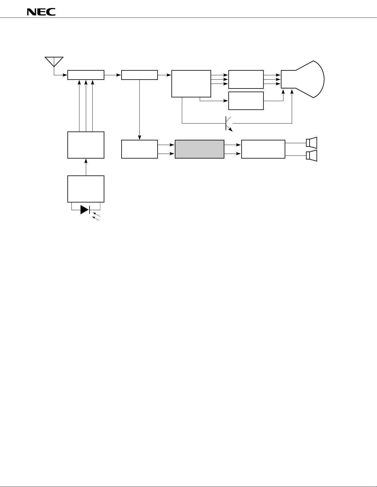
SYSTEM BLOCK DIAGRAM (TV)
µ
PC1892
PD17002
µ
PD17052
µ
PD17053
µ
PC2800A
µ
PC2801A
µ
Tuner PIF&SIF
Digital tuning
controller
PC1852
µ
Remote
control
reception
amplifier
PIN photo diode
US MTS
Color, intensity
and defrecting
signal processor
µ
L
R
PC1892
Matrix surround
sound processor
Color
output
Vertical
output
Power amplifier
PC1310
µ
PC1316C
µ
CRT
CRT
2
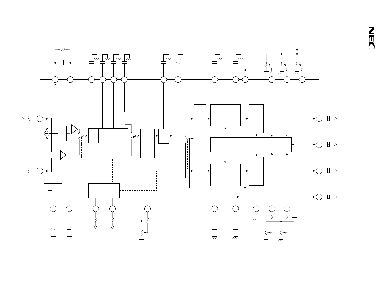
BLOCK DIAGRAM
L
R
IN
22 F
IN
22 F
HPF
820 kΩ
0.1 F
0.082 F
µ
28 29 2 3 4 5 30 22 21 1 20 19 18
+
25
µ
LPF
+
26
1
–
+
–
+
Movie/
Music
L–R
Simulated
2200 pF
µ
FC1 FC2 FC3 FC4
PS1
PHASE SHIFTER
µ
1
CC
V
2
+
µ
Note Recommended Precision: ±1 %
680 pF22 F
MODE
CONTROL
1 kΩ
0.022 F
PS2 PS3 PS4
Music
1 kΩ
MS2MS1
µ
0.022 F 1000 pF
µ
Simulated/Movie
10 kΩ
(L–R)
ϕ
+5 V
EFFECT
LPF
2
CONTROL
510 Ω
EFFECT
CONTROL
1 F
µ
+
6
Surround
OFFSET
ABSORPTION
OFF
1
V
CC
2
Note Note
6800 pF
MATRIX
Note Note
0.15 F V
TONE
(BASS, TREBLE)
CONTROL
TONE
(BASS, TREBLE)
CONTROL
0.15 F6800 pF
µ
DC CONTROL
µ
BALANCE
CONTROL
CC
10 kΩ
VOLUME
VOLUME
VOLUME
CONTROL
GND
10 kΩ
VOLUME
CONTROL
10 kΩ
510 Ω 510 Ω
BALANCE
CONTROL
BALANCE
CONTROL
1715111023872724
510 Ω
BASS
CONTROL
+5 V
10 kΩ
16
510 Ω
TREBLE
CONTROL
10 kΩ
L + R
VOLUME
CONTROL
510 Ω
+5 V
L OUTPUT
ϕ
L+ (L–R)
+
14
µ
4.7 F
REAR OUTPUT
ϕ
(L–R)
+
9
4.7 F
µ
R OUTPUT
ϕ
R– (L–R)
+
12
µ
4.7 F
L+R OUTPUT
L+R
+
13
4.7 F
µ
µ
PC1892
3
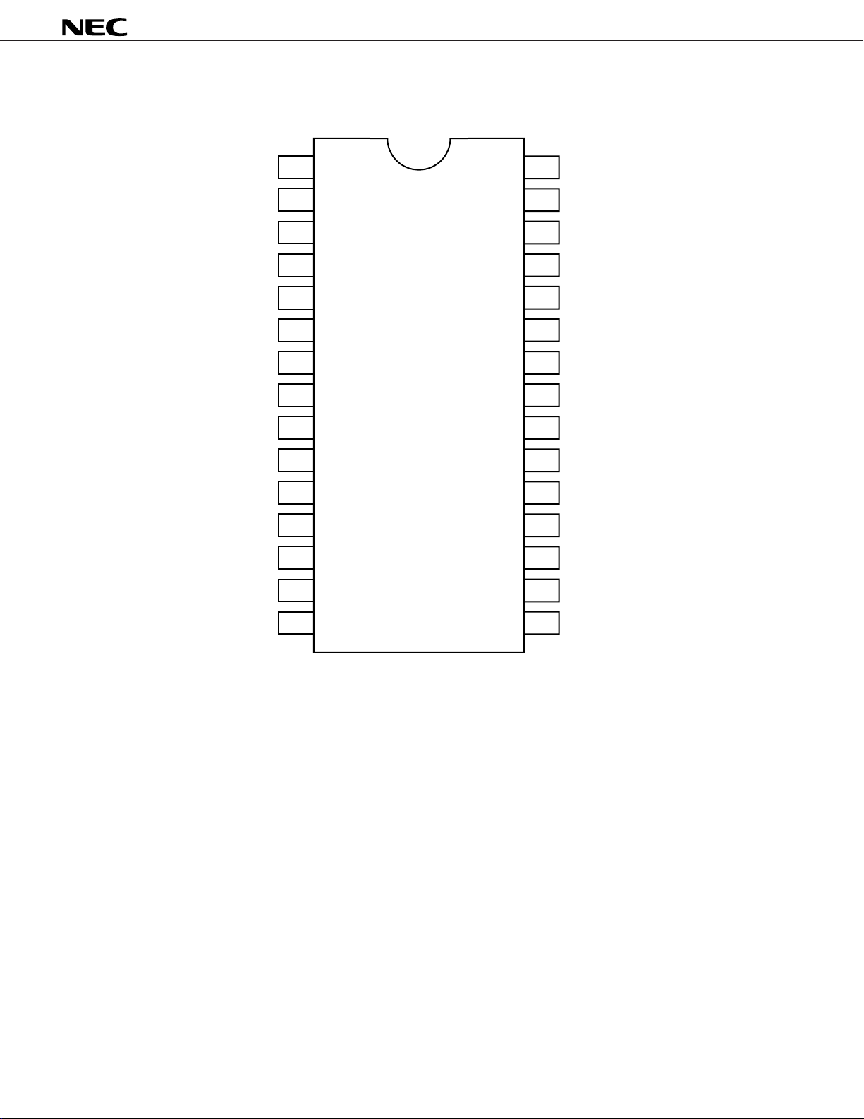
PIN CONFIGURATIONS (Top View)
µ
PC1892
30 Low Pass Filter2
1VCCSupply Voltage
LF2
2 FC1Phase Shift Filter1
3 FC2Phase Shift Filter2
4 FC3Phase Shift Filter3
5 FC4Phase Shift Filter4
6OFOffset Filter
µ
µ
PC1892CT
7 MS1Mode Select1
8 MS2Mode Select2
9 REARoutRear Output
10 RTCR-ch Treble Capacitor
11 RBCR-ch Bass Capacitor
12 RoutR-ch Signal Output
13 L + RoutL+R-ch Signal Output
14 LoutL-ch Signal Output
PC1892CT-02
29 Monaural Filter InputMFI
28 Monaural Filter OutputMFO
27 Low Pass Filter1LF1
IN
26 R-ch Signal InputR
25 L-ch Signal InputLIN
24 Reference VoltageRF
23 Effect ControlEFF
22 L-ch Treble CapacitorLTC
21 L-ch Bass CapacitorLBC
20 Balance ControlBAL
19 Volume ControlVOL
18 L+R-ch Volume ControlL + R
17 Bass ControlBAS
15 GNDGround
16 Treble ControlTBL
4

µ
PC1892
MODE SELECT CODE
Select among OFF, Movie, Music and Simulated mode by MS1 and MS2 (Pins 7 and 8).
Code MS1 MS2
Mode (Pin 7) (Pin 8)
OFF L L
Music H L
Movie L H
Simulated H H
Cautions 1. In the case of changing surround mode and power ON/OFF, mute (approx. 200 ms) must be used for pop
noise reduction.
2. Insert resistors between mode select pins (pin 7, 8) and GND, between control pins (pin 16, 17, 18, 19, 20,
23) and GND.
3. Connect a electrolytic capacitor for power supply as close as possible to V
Remark About "H" and "L", refer to RECOMMENDED OPERATING CONDITIONS.
CC (pin 1).
5
µ
PC1892
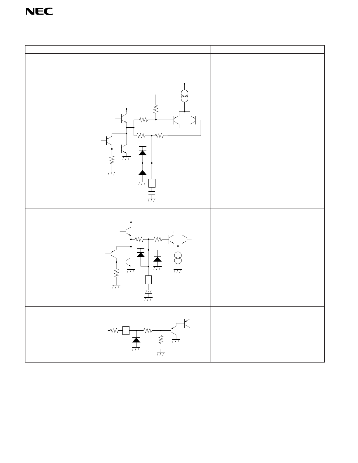
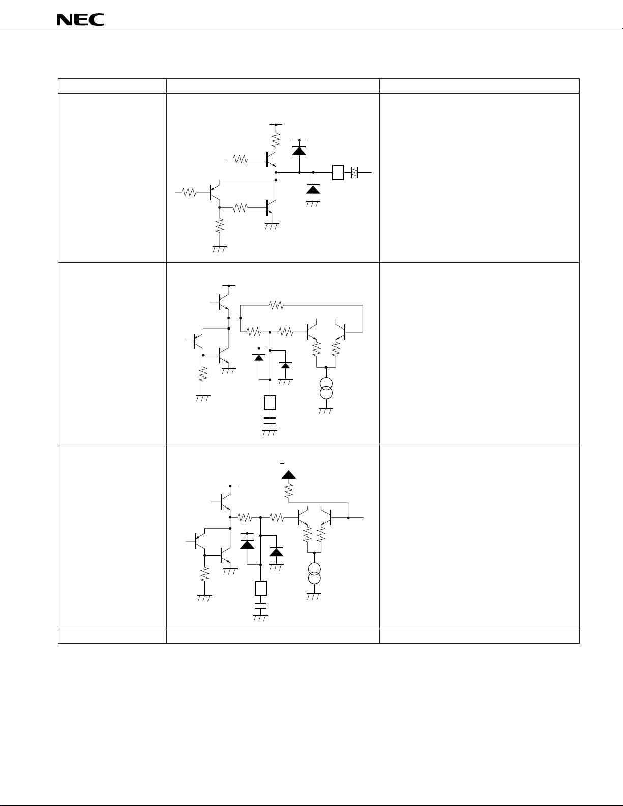
Explanation of Pins (1/4)
Pin number/name Equivalent circuit Description
1 Power supply VCC Power supply pin.
2 Phase shift filter1 (Pins 3, 4 and 5 are same as pin 2.) Capacitor connection pin which determines time
3 Phase shift filter2 constant of phase shifter.
V
4 Phase shift filter3 Pin 2 is used for movie, music, simulated mode.
5 Phase shift filter4 Pins 2, 3, 4, 5 is used for movie, simulated mode.
V
10 kΩ
CC
21 kΩ
18 kΩ 3 kΩ
V
CC
21 kΩ
CC
5 A
µ
Recommended value of capacitor is as follows.
Pin 2: 0.1 µF
Pin 3: 2200 pF
Pin 4, 5: 0.022 µF
2
6 Offset filter Capacitor connection pin which absorbs offset
10 kΩ
7 Mode select1 (Pin 8 is same as pin 7.) Surround mode switch pin.
8 Mode select2 Control by pin 7, 8 (2 bit parallel).
1 kΩ
V
CC
50 kΩ 3 kΩ
V
7
CC
50 kΩ
voltage generated by phase shifter.
µ
25 A
6
+
1 F
µ
–
Input impedance:approx. 100 kΩ.
50 kΩ
6
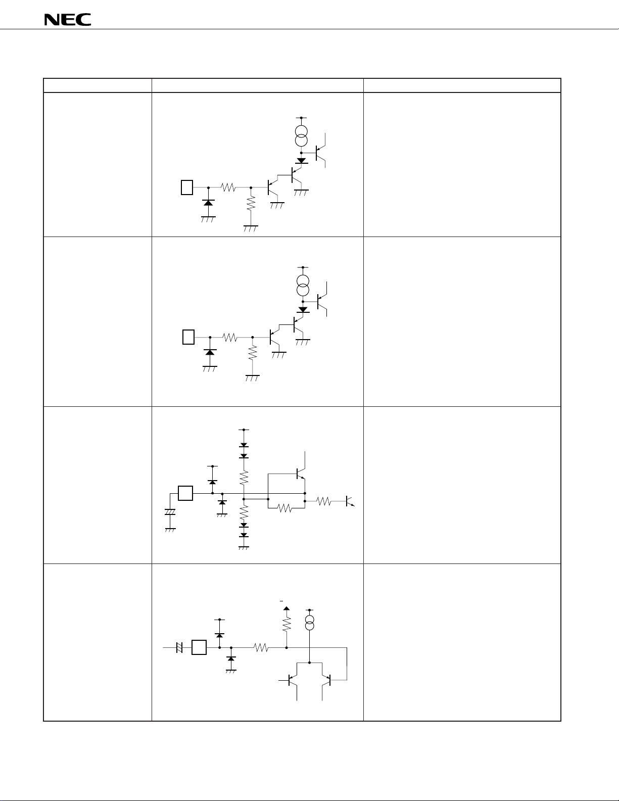
Explanation of Pins (2/4)
Pin number/name Equivalent circuit Description
9 Rear output (Pins 12, 13 and 14 are same as pin 9.)
12 R-ch signal output
13 L+R-ch signal output
14 L-ch signal output
5 kΩ
1 kΩ
V
CC
V
CC
4.7 F
µ
+
9
µ
PC1892
5 kΩ
5 kΩ
10 kΩ
10 R-ch treble capacitor (Pin 22 is same as pin 10.)
22 L-ch treble capacitor
V
CC
7.5 kΩ
5.8 kΩ 3 kΩ
V
CC
3 kΩ
3 kΩ
10 kΩ
25 A
µ
10
6800 pF
(±1 %)
11 R-ch bass capacitor (Pin 21 is same as pin 1.)
21 L-ch bass capacitor
V
CC
1
V
CC
2
7.5 kΩ
5.3 kΩ 3 kΩ
V
CC
3 kΩ
10 kΩ
3 kΩ
25 A
µ
11
0.15 F
µ
(±1 %)
15 GND GND GND pin.
7
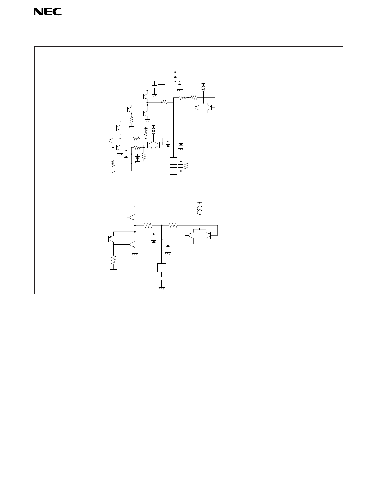
Explanation of Pins (3/4)
Pin number/name Equivalent circuit Description
16 Treble control (Pins 17, 18, 19 and 20 are same as pin 16.) Sound control pin.
17 Bass control
18 L+R-ch volume control
19 Volume control
20 Balance control
16
75 kΩ
75 kΩ
23 Effect control Surround effect control pin.
40 A
µ
40 A
µ
V
CC
V
CC
Input impedance: approx. 100 kΩ.
µ
PC1892
23
50 kΩ
50 kΩ
24 Reference voltage
V
CC
CC
V
20 kΩ
24
+
22 F
–
µ
20 kΩ
10 kΩ
3 kΩ
25 L-ch signal input (Pin 26 is same as pin 25.) Input impedance: approx. 40 kΩ.
26 R-ch signal input
1
VCC
2
CC
V
18.3 k
VCC
µ
Ω
5 A
+–
25
18.3 k
µ
22 F
Ω
8
µ
PC1892
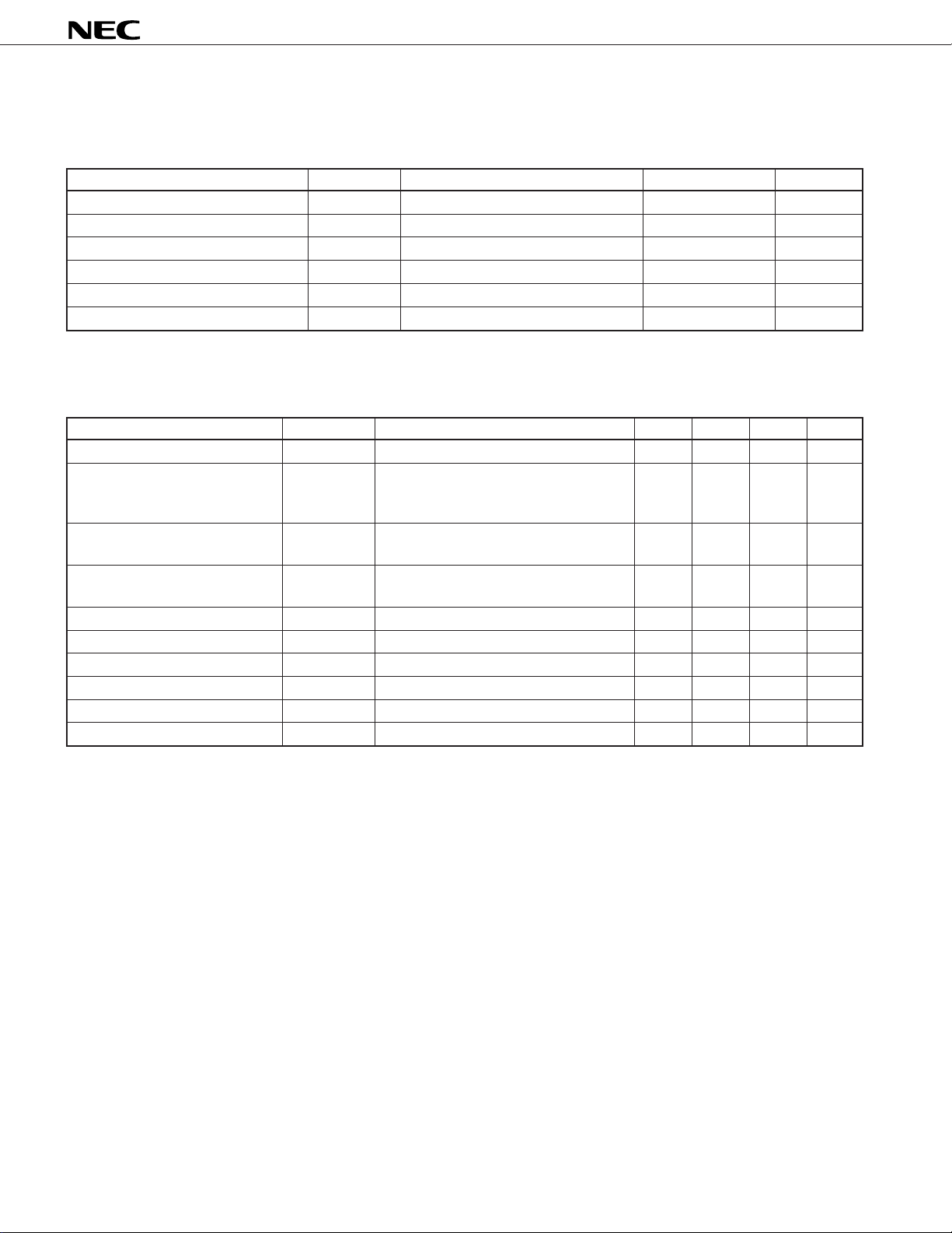
Explanation of Pins (4/4)
Pin number/name Equivalent circuit Description
27 Low pass filter1 Pins 28, 29 are for HPF at simulated mode.
28 Monaural filter output Connect capacitor and resistor between pin 28
29 Monaural filter input and 29.
V
CC
10
V
CC
1
Ω
k
V
V
CC
2
47
15 k
Ω
k
Ω
15 k
Ω
V
CC
47 k
10 k
Ω
1 k
CC
5 A
Ω
27
680 pF
Ω
µ
V
CC
V
28
29
CC
18 k
3 k
Ω
Ω
µ
0.082 F
820 k
V
CC
µ
5 A
Ω
30 Low pass filter2
10 k
V
V
CC
3 k
17.7 k
Ω
V
CC
Ω
CC
µ
5 A
Ω
30
1000 pF
9
µ
PC1892
ELECTRICAL CHARACTERISTICS
Absolute Maximum Ratings (at TA = 25 °C)
Parameter Symbol Conditions Ratings Unit
Supply voltage VCC No signal, OFF mode 14.0 V
Input signal level VIN Pin 25, 26 Input voltage VCC V
Control pin voltage VCONT Pin 16, 17, 18, 19, 20, 23 Apply voltage VCC + 0.2 V
Package power dissipation PD TA = 75 °C 640 mW
Operating temperature TA VCC = 12 V –20 to +75 °C
Storage temperature Tstg –40 to +125 °C
Recommended Operating Conditions
Parameter Symbol Conditions MIN. TYP. MAX. Unit
Supply voltage VCC No signal, OFF mode 10.8 12.0 13.2 V
VCC = 12 V, OFF mode, T.H.D = 1 %
Input signal level 1 VIN1 Volume control voltage = 5.0 V – 1.4 8.5 Vp-p
Balance, bass, treble control voltage = 2.5 V
Input signal level 2 VIN2 – 1.4 8.5 Vp-p
Output load impedance PL 10 kΩ
Mode select pin voltage (H) VMSH Pin 7, 8 Apply voltage 3.5 5.0 VCC V
Mode select pin voltage (L) VMSL Pin 7, 8 Apply voltage 0 0 2.0 V
Effect pin voltage (H) VEFFH Pin 23 Upper limit voltage – 5.0 VCC V
Effect pin voltage (L) VEFFL Pin 23 Lower limit voltage 0 0 – V
Control pin voltage (H) VCONTH Pin 16, 17, 18, 19, 20 Apply voltage – 5.0 VCC V
Control pin voltage (L) V CONTL Pin 16, 17, 18, 19, 20 Apply voltage 0 0 – V
VCC = 12 V, T.H.D = 1 %
L+R volume control voltage = 5.0 V
AC load impedance which can be driven
by output of pin 9, 12, 13, 14
10
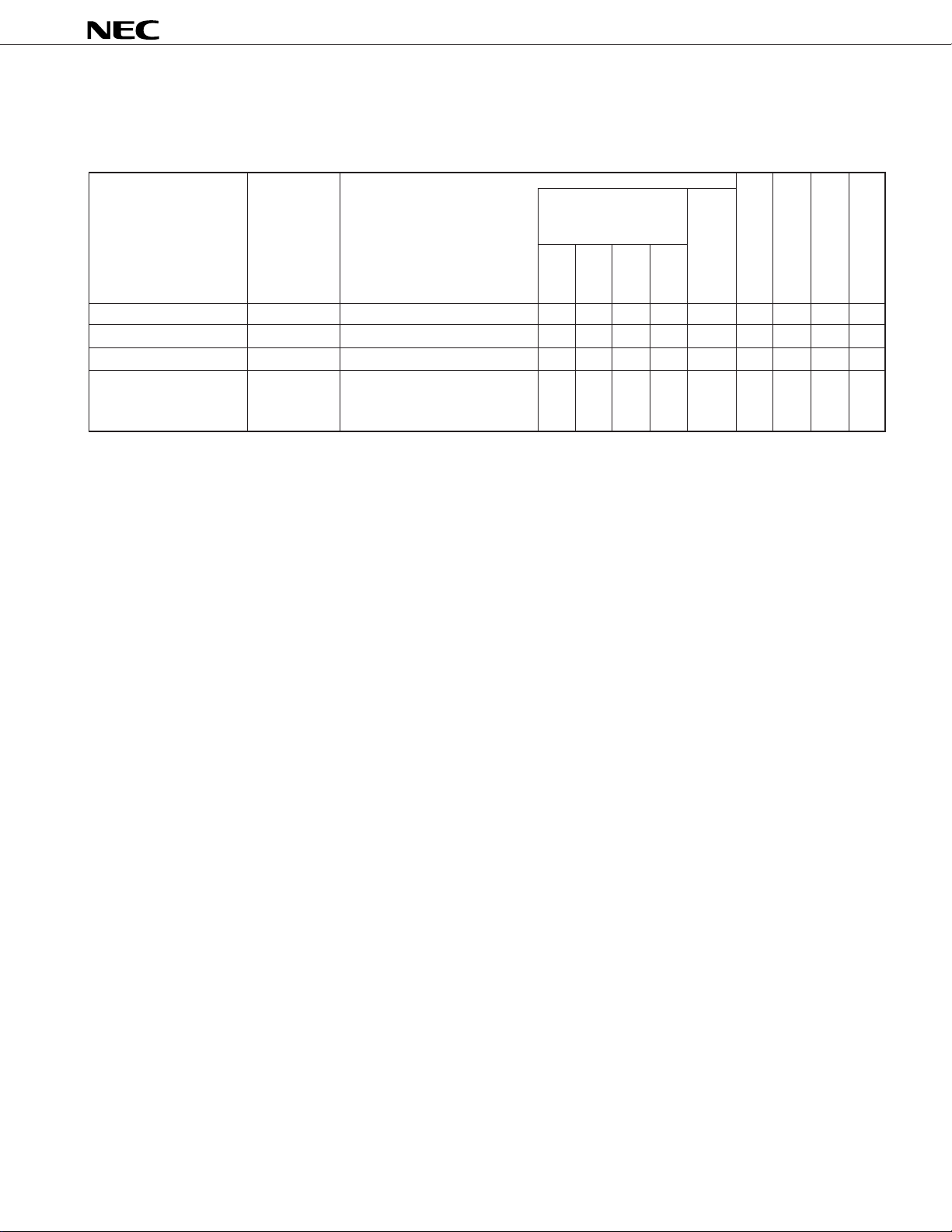
Electrical characteristics (TA = 25 °C, RH ≤ 70 %, VCC = 12 V)
General
µ
PC1892
Parameter Symbol Test conditions
Supply current ICC No signal – – – – OFF 23 29 37 mA
Maximum output voltage VOM VCC = 12 V, T.H.D. = 1 % H M M M OFF 8.5 9.9 Vp-p
Distortion factor T.H.D. VIN = 0.5 Vr.m.s., f = 1 kHz H M M M OFF – 0.1 0.5 %
L+R distortion factor T.H.D. (L+R) VIN = 0.5 Vr.m.s., f = 1 kHz, – – – – – – 0.1 0.5 %
L+R volume control voltage:
5.0 V
Note 1
Control pin voltage
(V)
Balance
Treble
Volume
Note 1
Bass
MIN. TYP. MAX. Unit
Note 2
Surround mode
Note 1. H: 5.0 V, M: 2.5 V, L: 0 V, –: Undefined
2. OFF: OFF mode, –: Undefined
11
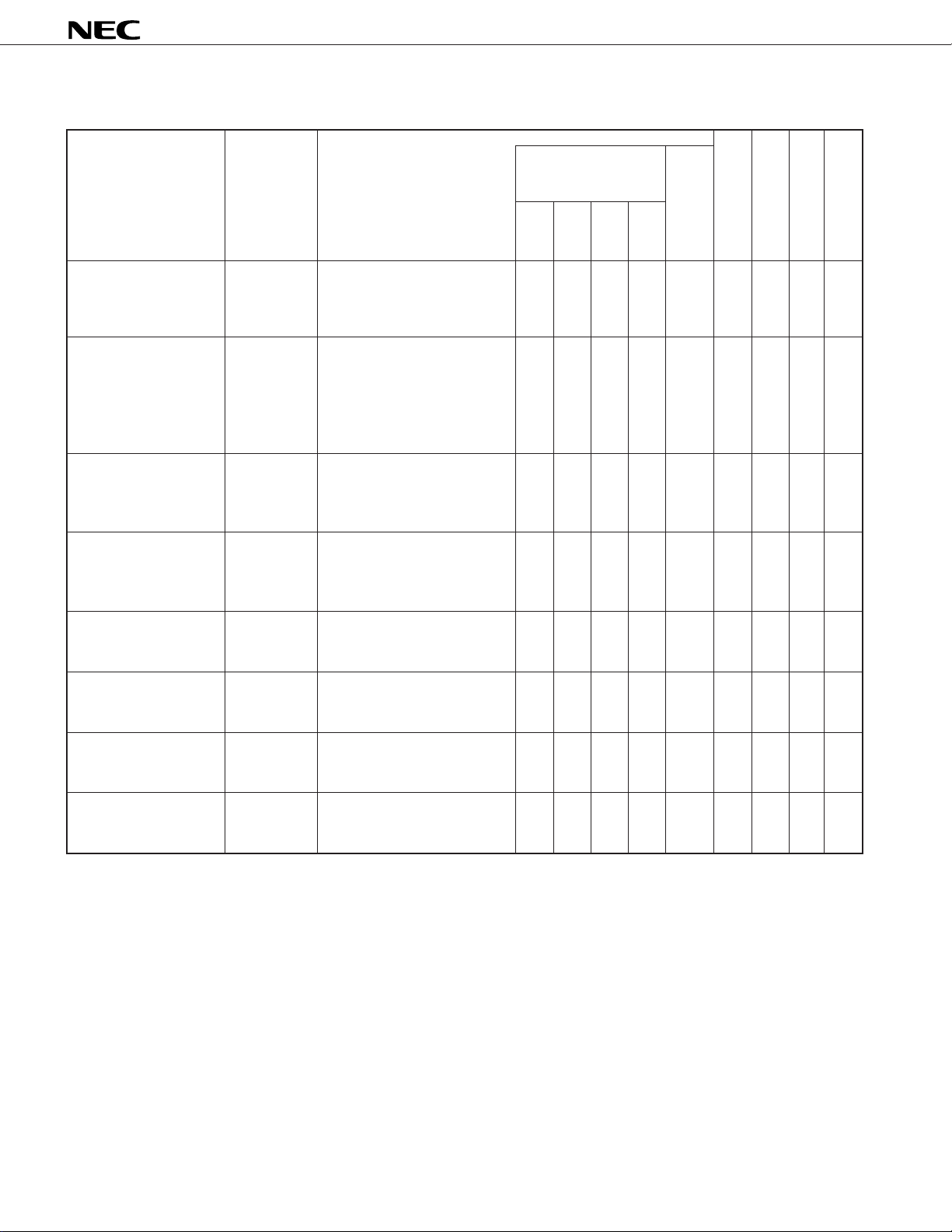
µ
PC1892CT Volume control, tone control block (1/1)
µ
PC1892
Parameter Symbol Test conditions
Volume attenuation ATTVOL VIN = 0.5 Vr.m.s., f = 1 kHz, H M M M OFF – –80 –72 dB
Volume control voltage: 0.2 V ↓
0 dB: Volume control voltage = H 0.2
Filter: JIS-A
L+R volume attenuation ATTL+RVOL VIN = 0.5 Vr.m.s., f = 1 kHz, – – – – – – –85 –75 dB
L+R volume control voltage:
0.2 V
0 dB: L+R volume control
voltage = H
Filter: JIS-A
Balance attenuation L-ch ATTBALL V IN = 0.5 Vr.m.s., f = 1 kHz, H M M M OFF –22 –18 –12 dB
Balance control voltage: 4.5 V ↓
0 dB: Balance control voltage = M 4. 5
Filter: JIS-A
Balance attenuation R-ch ATTBALR VIN = 0.5 Vr.m.s., f = 1 kHz, H M M M OFF –22 –18 –12 dB
Balance control voltage: 0.5 V ↓
0 dB: Balance control voltage = M 0. 5
Filter: JIS-A
Low-band boost control VBB VIN = 0.5 Vr.m.s., f = 100 Hz, H M M M OFF 7 10 13 dB
Bass control voltage: 4.5 V ↓
0 dB: Bass control voltage = M 4.5
Low-band cut control VBC VIN = 0.5 Vr.m.s., f = 100 Hz, H M M M OFF –13 –10 –7 dB
Bass control voltage: 0.5 V ↓
0 dB: Bass control voltage = M 0.5
High-band boost control VTB VIN = 0.5 Vr.m.s., f = 10 kHz, H M M M OFF 7 10 13 dB
Treble control voltage: 4.5 V ↓
0 dB: Treble control voltage = M 4.5
High-band cut control VTC VIN = 0.5 Vr.m.s., f = 10 kHz, H M M M OFF –13 –10 –7 dB
Treble control voltage: 0.5 V ↓
0 dB: Treble control voltage = M 0.5
Note 1
Control pin voltage
(V)
Volume
Balance
Note 1
Treble
Note 2
Bass
MIN. TYP. MAX. Unit
Surround mode
Note 1. H: 5.0 V, M: 2.5 V, L: 0 V, –: Undefined, The alphanumeric numbers in this table represent the level (V).
2. OFF: OFF mode, –: Undefined
12
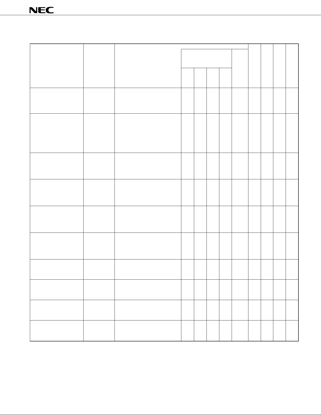
µ
PC1892CT-02 Volume control, tone control block (1/1)
µ
PC1892
Parameter Symbol Test conditions
Volume attenuation ATTVOL VIN = 0.5 Vr.m.s., f = 1 kHz, H M M M OFF – – –90 dB
Volume control voltage: 0.2 V ↓
0 dB: Volume control voltage = H 0.2
Filter: JIS-A
L+R volume attenuation ATTL+RVOL VIN = 0.5 Vr.m.s., f = 1 kHz, – – – – – – –85 –75 dB
L+R volume control voltage:
0.2 V
0 dB: L+R volume control
voltage = H
Filter: JIS-A
Balance attenuation 1 ATTBALL1 VIN = 0.5 Vr.m.s., f = 1 kHz, H M M M OFF –19 –16 –10 dB
L-ch Balance control voltage: 4.3 V ↓
0 dB: Balance control voltage = M 4. 3
Filter: JIS-A
Balance attenuation 2 ATTBALL2 VIN = 0.5 Vr.m.s., f = 1 kHz, H M M M OFF – – –90 dB
L-ch Balance control voltage: 5 V ↓
0 dB: Balance control voltage = M 5. 0
Filter: JIS-A
Balance attenuation 1 ATTBALR1 VIN = 0.5 Vr.m.s., f = 1 kHz, H M M M OFF –19 –16 –10 dB
R-ch Balance control voltage: 0.7 V ↓
0 dB: Balance control voltage = M 0. 7
Filter: JIS-A
Balance attenuation 2 ATTBALR2 VIN = 0.5 Vr.m.s., f = 1 kHz, H M M M OFF – – –90 dB
R-ch Balance control voltage: 0 V ↓
0 dB: Balance control voltage = M 0. 0
Filter: JIS-A
Low-band boost control VBB VIN = 0.5 Vr.m.s., f = 100 Hz, H M M M OFF 7 10 13 dB
Bass control voltage: 4.5 V ↓
0 dB: Bass control voltage = M 4.5
Low-band cut control VBC VIN = 0.5 V r.m.s., f = 100 Hz, H M M M OFF –13 –10 –7 dB
Bass control voltage: 0.5 V ↓
0 dB: Bass control voltage = M 0.5
High-band boost control VTB VIN = 0.5 Vr.m.s., f = 10 kHz, H M M M OFF 7 10 13 dB
Treble control voltage: 4.5 V ↓
0 dB: Treble control voltage = M 4.5
High-band cut control VTC VIN = 0.5 Vr.m.s., f = 10 kHz, H M M M OFF –13 –10 –7 dB
Treble control voltage: 0.5 V ↓
0 dB: Treble control voltage = M 0.5
Note 1
Control pin voltage
(V)
Balance
Treble
Volume
Note 1
Bass
MIN. TYP. MAX. Unit
Note 2
Surround mode
Note 1. H: 5.0 V, M: 2.5 V, L: 0 V, –: Undefined, The alphanumeric numbers in this table represent the level (V).
2. OFF: OFF mode, –: Undefined
13
 Loading...