NEC PS9634, PS9634L, PS9634L-E3 Datasheet

DATA SHEET
©
PHOTOCOUPLER
PS9634,PS9634L
POWER TRANSISTOR DRIVING
BASE AMPLIFIER BUILT-IN TYPE PHOTOCOUPLER
DESCRIPTION
The PS9634 and PS9634L are optical linkage devices mounting a GaAs infrared ray LED on the light emitting side
(input side) and a photo diode and a signal processing circuit on the light receiving side (output side) on one chip.
They can directly drive a power transistor of 15 to 20 A class used for such as an inverter control air conditioner or
general purpose inverter.
The PS9634L has a surface mount type lead.
FEATURES
• High instantaneous common mode rejection voltage (CMH = –1 000 V/µs MIN., CML = 1 000 V/µs MIN.)
• High supply voltage (VCC = 18 V)
PHL
• High-speed response (t
• High output current (IO1 = 0.5 A (DC), I
• Taping product name (PS9634L-E3, E4)
PLH
, t
= 5 µs MAX.)
O1P
= 1.0 A (pulse) )
APPLICATIONS
• Inverter control air conditioner
• General purpose inverter
The information in this document is subject to change without notice.
Document No. P12686EJ4V0DS00 (4th edition)
Date Published February 1998 NS CP(K)
Printed in Japan
The mark
••••
shows major revised points.
1992

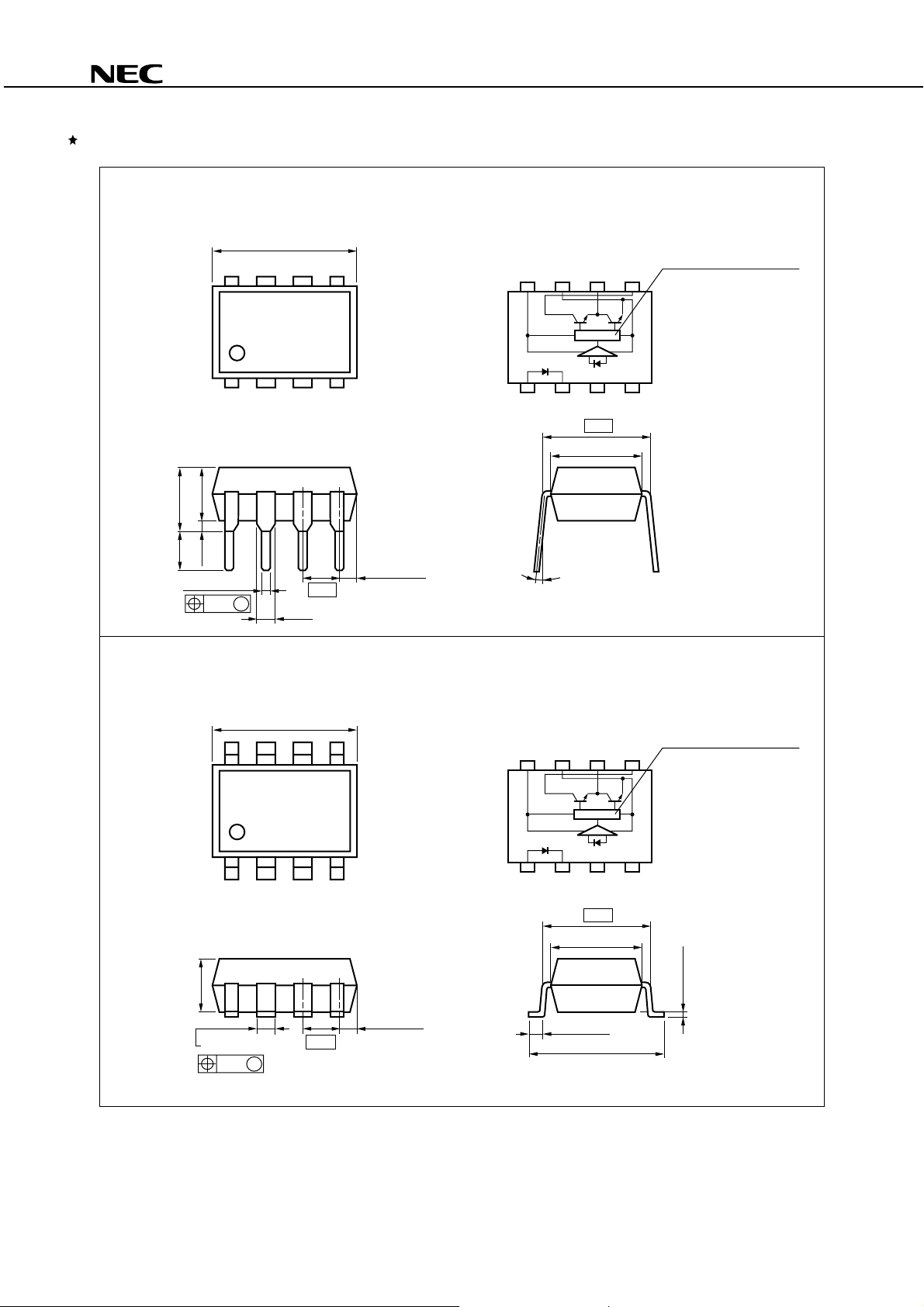
PACKAGE DIMENSIONS (in millimeters)
PS9634,PS9634L
PS9634
3.8 MAX.
4.55 MAX.
0.65
2.8 MIN.
0.50±0.10
0.25 M
10.16 MAX.
1.34
2.54
1.27 MAX.
PS9634L
TOP VIEW
8765
Tr.1 Tr.2
1234
7.62
6.5±0.5
0 to 15˚
Signal processing circuit
1. Anode
2. Cathode
3. NC
4. NC
5. Output (O1)
6. Output (O2)
7. GND
8. V
CC
3.8 MAX.
1.34±0.10
0.25 M
10.16 MAX.
2.54
1.27 MAX.
TOP VIEW
8765
Tr.1 Tr.2
1234
7.62
6.5±0.5
0.9±0.25
9.60±0.4
Signal processing circuit
1. Anode
2. Cathode
3. NC
4. NC
5. Output (O1)
6. Output (O2)
7. GND
CC
8. V
0.05 to 0.2
2

ABSOLUTE MAXIMUM RATINGS (TA = 25 °°°°C, unless otherwise specified)
Parameter Symbol Ratings Unit
PS9634,PS9634L
I
O1P
O2P
F
R
FM
CC
O1
O2
O1
O
30 mA
6.0 V
1A
18 V
0.5 A
1.0
0.8
2.0
18 V
500 mW
BV 5 000 Vr.m.s.
T
A
stg
550 mW
−
20 to +80
−
55 to +150
°
C
°
C
Diode Forward Current (DC) I
Reverse Voltage V
Peak Forward Current
*1
Detector Supply Voltage V
Output Current (O1) I
Peak Output Current (O1) I
Output Current (O2) I
Peak Output Current (O2) I
Output Voltage (O1) V
Power Dissipation P
Isolation Voltage
*2
Total Power Dissipat i on P
Operating Ambient Temperature T
Storage Temperature T
PW = 100
*1
AC voltage for 1 minute at TA = 25 °C, RH = 60 % between input and output
*2
s, Duty Cycle = 1 %
µ
RECOMMENDED OPERATING CONDITIONS TRUTH TABLE
Parameter Symbol MIN. TYP. MAX. Unit LED
Input On Current I
Supply Voltage V
Output Current (O1) I
Output Current (O2) I
Operating Ambient Temperature T
FLH
O1
O2
6 8 10 mA ON OFF
CC
5.4 15 V Tr. 1 ON OFF
0.1 0.2 0.3 A Tr. 2 OFF ON
A
02550
°
C
3

PS9634,PS9634L
ELECTRICAL CHARACTERISTICS (TA = −−−−20 to +80 °°°°C, unless otherwise specified)
Parameter Symbol Conditions MIN. TYP. MAX. Unit Fig.
Diode Forward Voltage V
Reverse Current I
Terminal Capacitance C
Detector Supply Voltage V
Low Level Output Voltage
V
(O1)
High Level Output Voltage
V
(O2)
Low Level Output Voltage
V
(O2)
Leakage Current (O1) I
Leakage Current (O2) I
High Level Supply Current I
Low Level Supply Current I
Coupled Input On Current (L → H) I
Isolation Resistance R
Propagation Delay Time
(L → H)
Propagation Delay Time
(H → L)
Instantaneous Common
CM
Mode Rejection Voltage
(Output: High)
Instantaneous Common
CM
Mode Rejection Voltage
(Output: Low)
F
IF = 5 mA, TA = 25 °C1.11.4V
R
VR = 5 V, TA = 25 °C5
t
V = 0 V, f = 1.0 MHz, TA = 25 °C30pF
CC
VCC = 6 V, IO1 = 0.4 A, RL2 = 10 Ω,
O1L
F
= 5 mA
I
O2H
VCC = 6 V, IO2 = −0.4 A, IF = 5 mA 4.5 5.0 V 2
O2L
VCC = 6 V, IO2 = 0.5 A, IF = 0 mA 0.25 0.40 V
O1L
VCC = 13 V, IF = 0 mA 100
O2L
VCC = 13 V, IF = 5 mA 100
CCH
CC
V
= 6 V, IF = 5 mA 16
CCL
CC
V
= 6 V, IF = 0 mA 22
FLH
VCC = 6 V, RL1 = 5 Ω, RL2 = 10
I-O
RH = 40 to 60 %, TA = 25 °C10
VCC = 6 V, IF = 5 mA, TA = 25 °C
PLH
t
t
PHL
L1
= 5 Ω, RL2 = 10
R
TA = 25 °C, VCM = 600 V (peak),
H
F
= 5 mA, RL1 = 470 Ω, RL2 = 1 k
I
∆
V02H = 2 V
TA = 25 °C, VCM = 600 V (peak),
L
F
= 0 mA, RL1 = 470 Ω, RL2 = 1 k
I
∆
V02L = 0.5 V
TA = 25 °C812mA
TA = 25 °C1518mA
TA = 25 °C 0.3 1.5 3.0 mA 5
Ω
Ω
5.4 15 V
0.25 0.40 V 1
0.2 5.0
11
35
−
1 000 V/
Ω,
1 000 V/
Ω,
µ
A
µ
A3
µ
A4
Ω
µ
s6
µ
s7
µ
s
4
 Loading...