

Page 1

USER'S MANUAL
µ
PD78214 SUB-SERIES
8-BIT SINGLE-CHIP MICROCOMPUTER
HARDWARE
µ
PD78212
µ
PD78213
µ
PD78214
µ
PD78P214
µ
PD78212 (A)
µ
PD78213 (A)
µ
PD78214 (A)
µ
PD78P214 (A)
NEC Corporation 1989
Document No. IEU-1236H
(O. D. No. IEM-5119H)
Date Published September 1994 P
Printed in Japan
Page 2

GENERAL
1
PIN FUNCTIONS
CPU FUNCTION
CLOCK GENERATOR
PORT FUNCTIONS
REAL-TIME OUTPUT FUNCTION
TIMER/COUNTER UNITS
A/D CONVERTER
ASYNCHRONOUS SERIAL INTERFACE
CLOCK SYNCHRONOUS SERIAL INTERFACE
EDGE DETECTION FUNCTION
INTERRUPT FUNCTIONS
LOCAL BUS INTERFACE FUNCTION
STANDBY FUNCTION
2
3
4
5
6
7
8
9
10
11
12
13
14
RESET FUNCTION
APPLICATION EXAMPLES
PROGRAMMING FOR THE
INSTRUCTION OPERATIONS
78K/II SERIES PRODUCT LIST
DEVELOPMENT TOOLS
SOFTWARE FOR EMBEDDED APPLICATIONS
REGISTER INDEX
µ
PD78214
INDEX
15
16
17
18
A
B
C
D
E
Page 3

Cautions on CMOS Devices
1 Countermeasures against static electricity for all MOSs
Caution When handling MOS devices, take care so that they are not electrostatically charged.
Strong static electricity may cause dielectric breakdown in gates. When transporting or
storing MOS devices, use conductive trays, magazine cases, shock absorbers, or metal
cases that NEC uses for packaging and shipping. Be sure to ground MOS devices during
assembling. Do not allow MOS devices to stand on plastic plates or do not touch pins.
Also handle boards on which MOS devices are mounted in the same way.
2 CMOS-specific handling of unused input pins
Caution Hold CMOS devices at a fixed input level.
Unlike bipolar or NMOS devices, if a CMOS device is operated with no input, an
intermediate-level input may be caused by noise. This allows current to flow in the CMOS
device, resulting in a malfunction. Use a pull-up or pull-down resistor to hold a fixed input
level. Since unused pins may function as output pins at unexpected times, each unused
pin should be separately connected to the V
If handling of unused pins is documented, follow the instructions in the document.
3 Statuses of all MOS devices at initialization
Caution The initial status of a MOS device is unpredictable when power is turned on.
Since characteristics of a MOS device are determined by the amount of ions implanted
in molecules, the initial status cannot be determined in the manufacture process. NEC
has no responsibility for the output statuses of pins, input and output settings, and the
contents of registers at power on. However, NEC assures operation after reset and items
for mode setting if they are defined.
When you turn on a device having a reset function, be sure to reset the device first.
DD or GND pin through a resistor.
EWS-4800 Series, EWS-UX/V, and QTOP are trademarks of NEC Corporation.
MS-DOS is a trademark of Microsoft Corporation.
IBM DOS, PC/AT, and PC DOS are trademarks of IBM Corporation.
SPARCstation is a trademark of SPARC International, Inc.
Sun OS is a trademark of Sun Microsystems Inc.
HP9000 Series 300 and HP-UX are trademarks of Hewlett-Packard.
Page 4

The information in this document is subject to change without notice.
No part of this document may be copied or reproduced in any form or by any means without the prior written
consent of NEC Corporation. NEC Corporation assumes no responsibility for any errors which may appear in
this document.
NEC Corporation does not assume any liability for infringement of patents, copyrights or other intellectual
property rights of third parties by or arising from use of a device described herein or any other liability arising
from use of such device. No license, either express, implied or otherwise, is granted under any patents,
copyrights or other intellectual property rights of NEC Corporation or others.
The devices listed in this document are not suitable for use in aerospace equipment, submarine cables, nuclear
reactor control systems and life support systems. If customers intend to use NEC devices for above applications
or they intend to use "Standard" quality grade NEC devices for applications not intended by NEC, please contact
our sales people in advance.
Application examples recommended by NEC Corporation
Standard: Computer, Office equipment, Communication equipment, Test and Measurement equipment,
Machine tools, Industrial robots, Audio and Visual equipment, Other consumer products, etc.
Special: Automotive and Transportation equipment, Traffic control systems, Antidisaster systems, Anticrime
systems, etc.
M7 92.6
Page 5

Main Revisions in This Edition
Page Description
P.55 V
P.329
P.383 "Caution" has been added in (b) of Section
P.429 Appendix B has been modified as follows:
P.441 Appendix C has been added.
Major changes in this revision are indicated by stars (★)
in the margins.
and "Caution" have been added in (a) of Fig.
SS
4-2.
"Caution" has been added in (2) of Section 12.4.6.
14.4.2.
• "IBM PC series" has been changed to "IBM
PC/AT."
• Upgraded versions of MS-DOS are now
supported by some development tools
designed for the PC-9800 series.
• 3.5" 2HC has been added to as a PC DOS
distribution media.
• MS DOS and IBM DOS have been added
as supported operating systems for the
IBM PC/AT.
• The description of real-time OS has been
deleted.
Page 6

PREFACE
Users:
This manual is aimed at engineers who need to be familiar with the capabilities of the µPD78214 sub-series for
application program development purposes.
Purpose:
The purpose of this manual is to help users understand the hardware capabilities of the µPD78214 sub-series.
Organization:
Two manuals are available for the µPD78214 sub-series: The hardware manual (this manual) and instruction
manual (common to all 78K/II series products). The contents of the manuals are:
Hardware Instruction
Pin functions CPU functions
Internal block functions Addressing
Interrupt functions Instruction set
Other built-in functions
Important information related to using the products described in this manual is provided in the form of
“Caution” notes, appearing in appropriate places in each chapter. Each “Caution” is repeated at the end
of the chapter. Be careful to observe these notes when using the products.
Guidance:
Readers of this manual are assumed to have a general knowledge of electronics, logical circuits, and microcomputers.
When using this manual with the µPD78212, µPD78213, µPD78P214, µPD78212(A), µPD78213(A), µPD78214(A), or
µ
PD78P214(A):
This manual describes the functions of the µPD78212, µPD78213, µPD78214, µPD78P214, µPD78212(A), µPD78213(A),
µ
PD78214(A), and µPD78P214(A). The relationships between these products are shown in the figure on the next
page. Where there is no functional difference between the products, only the µPD78214 is described, that
description also being applicable to the µPD78212, µPD78213, µPD78P214, µPD78212(A), µPD78213(A), µPD78214(A),
and µPD78P214(A).
The examples given in this manual are prepared for “Standard” quality products for general electronics
devices. If customers intend to use the examples in this manual in fields where the “Special” quality is
required, note the quality grade of the parts and circuits actually used.
Page 7

PD78P214
µ
PD78P214(A)
µ
PROM 16K
RAM 512
PD78214
µ
PD78214(A)
µ
PD78212
µ
PD78212(A)
µ
ROM 16K
RAM 512
ROM 8K
RAM 384
PD78213
µ
PD78213(A)
µ
ROM-less
RAM 512
To check the details of a register when you know the name of the register:
See Appendix D.
To check the differences between the µPD78214 sub-series and other models of the 78K/II series:
First see Appendix A to determine the differences between the models then see Appendix E for details.
To check the details of a function when you know the name of the function:
See Appendix E.
If the microcomputer does not operate correctly during debugging:
See the cautions at the end of the chapter related to the erroneous function.
To become familiar with the general functions of the µPD78214 sub-series:
Read the entire manual in the order of the table of contents.
To determine the instructions supported by the µPD78214 sub-series in detail:
Refer to 78K/II Series User’s Manual, Instruction (IEU-1311).
To determine the electrical characteristics of the µPD78214 sub-series:
Refer to the separate data sheet.
Application examples of the µPD78214 sub-series:
Refer to the separate application note.
Notation:
Data weight: High-order digits on the left side
Low-order digits on the right side
Active low: ××× (Pins and signal names are overscored.)
Note: Explanation of a noted part of text
Caution: Information demanding the user's special attention
Remarks: Supplementary information
Numeric value: Binary : ××××B or ××××
Decimal : ××××
Hexadecimal : ××××H
Page 8

Register representation
7
6
5
4
3
2
1
0
EDC
Register name
B
1
0
×
A
1
0
The encircled bit number indicates that the bit name
×
is used as reserved word by the NEC assembler and
defined by the header file, sfrbit.h, by C compiler.
Write operation Read operation
Either 0 or 1 can be
written to this bit without
affecting the register
operation.
Write 0 to this bit.
Write 1 to this bit.
Write a value according to
the necessary function.
Never use the code combinations indicated "Not to be set" in the register descriptions.
Characters likely to be confused: 0 (zero) and O (uppercase "O")
1 (one), l (lowercase "L"), and I (uppercase "I")
Related documents:
The following reference documents are also available.
0 or 1 is read from these
bits.
A value is read according
to the operation.
• Documents related to the µPD78214 sub-series
Product
Document
Data Sheet
User's Manual Hardware
Instruction
Application Note Basic
Application
Floating-Point Arithme-
tic Operation Programs
• Serial Bus Interface (SBI) User’s Manual (IEM-1303)
µ
PD78212
µ
PD78213
µ
PD78214
IC-2526 IC-2831 IC-3095
µ
PD78212(A)
µ
PD78213(A)
µ
PD78214(A)
This manual
IEU-1311
IEA-1220
IEA-1282
IEA-1273
µ
PD78P214(A)
Page 9

• Documents related to development tools
Document name
IE-78240-R-A In-Circuit Emulator User's Manual
IE-78240-R In-Circuit Emulator User's Manual Hardware
IE-78210-R In-Circuit Emulator Hardware Operator's Manual
IE-78210-R In-Circuit Emulator Software Operator's Manual
IE-78210-R In-Circuit Emulator System
Software Operator's Manual
RA78K Series Assembler Package User's Manual Language
78K Series Structured Assembler Preprocessor User's Manual
CC78K Series C Compiler User's Manual
SD78K/II Screen Debugger User's Manual for Operation under
MS-DOS Tutorial
78K/II Series Development Tools Selection Guide
For Operation on the PC-9800 Series (MS-DOS)
For Operation on the IBM PC Series (PC DOS)
• Documents related to software to be incorporated into the product
Software
Operation
Language
Operation
Document No.
EEU-1395
EEU-1322
EEU-1331
EEP-1027
EEM-1024
EEM-1260
EEM-1027
EEU-1283
EEU-1273
EEU-1254
EEU-1289
EEU-1280
EEU-1447
EEU-1413
EF-1114
Document name
Fuzzy Inference Development Support System Pamphlet
78K/II Series Fuzzy Inference Development Support System User's
Manual
78K/0, 78K/II and 87AD Series Fuzzy Inference Development Support
System User's Manual
User's Manual for Tool for Creating Fuzzy Knowledge Data
Fuzzy Inference
Module
Translator
Document No.
EF-1113
EEU-1448
EEU-1444
EEU-1438
Page 10

• Other documents
Document name
Package Manual
SMD Surface Mount Technology Manual
Quality Grades on NEC Semiconductor Devices
NEC Semiconductor Device Reliability/Quality Control System
Guide to Quality Assurance for Semiconductor Devices
Caution The above documents may be revised without notice. Use the latest versions when you designing an application system.
Document No.
IEI-1213
IEI-1207
IEI-1209
IEI-1203
MEI-1202
Page 11

Page 12

Contents
CONTENTS
CHAPTER 1 GENERAL ........................................................................................................................................1
1.1 FEATURES ............................................................................................................................3
1.2 ORDERING INFORMATION AND QUALITY GRADE ........................................................4
1.2.1 Ordering Information ................................................................................................. 4
1.2.2 Quality Grade ............................................................................................................. 5
1.3 PIN CONFIGURATION (TOP VIEW) ....................................................................................6
1.3.1 Normal Operating Mode ...........................................................................................6
1.3.2 PROM Programming Mode ...................................................................................... 11
1.4 EXAMPLE APPLICATION SYSTEM (PRINTER) ................................................................. 16
1.5 BLOCK DIAGRAM ................................................................................................................ 17
1.6 FUNCTIONS ..........................................................................................................................18
1.7 DIFFERENCES BETWEEN THE µPD78210 AND µPD78213 .............................................20
1.8
DIFFERENCES BETWEEN THE µPD78214 SUB-SERIES AND µPD78218A SUB-SERIES ......
1.9 DIFFERENCES BETWEEN THE µPD78212 AND µPD78212(A) ........................................22
1.10 DIFFERENCES BETWEEN THE µPD78213 AND µPD78214, AND THE µPD78213(A)
AND µPD78214(A) ................................................................................................................22
1.11 DIFFERENCES BETWEEN THE µPD78P214 AND µPD78P214(A) .................................... 22
1.12 DIFFERENCES BETWEEN THE µPD78212, µPD78213, µPD78214, AND µPD78P214 ...23
1.12.1 Functional Differences ...........................................................................................23
1.12.2 Package Differences ...............................................................................................23
21
CHAPTER 2 PIN FUNCTIONS ............................................................................................................................ 25
2.1 PIN FUNCTION LIST ............................................................................................................25
2.1.1 Normal Operating Mode ...........................................................................................25
2.1.2 PROM Programming Mode ...................................................................................... 27
2.2 PIN FUNCTIONS ...................................................................................................................27
2.2.1 Normal Operating Mode ...........................................................................................27
2.2.2 PROM Programming Mode ...................................................................................... 31
2.3 I/O CIRCUITS AND UNUSED-PIN HANDLING ..................................................................33
2.4 NOTES ...................................................................................................................................35
CHAPTER 3 CPU FUNCTION ............................................................................................................................. 37
3.1 MEMORY SPACE ................................................................................................................. 37
3.1.1 Internal Program Memory Area ...............................................................................42
3.1.2 Internal RAM Area ..................................................................................................... 43
3.1.3 Special Function Register (SFR) Area .....................................................................43
3.1.4 External SFR Area ......................................................................................................43
3.1.5 External Memory Space ............................................................................................ 43
3.1.6 External Extension Data Memory Space ................................................................43
3.2 REGISTERS ...........................................................................................................................45
3.2.1 Program Counter (PC) ...............................................................................................45
3.2.2 Program Status Word (PSW) ....................................................................................45
3.2.3 Stack Pointer (SP) ...................................................................................................... 46
3.2.4 General-Purpose Registers .......................................................................................47
3.2.5 Special Function Registers (SFR) ............................................................................. 50
- i -
Page 13

Contents
3.3 NOTES ...................................................................................................................................53
CHAPTER 4 CLOCK GENERATOR .....................................................................................................................55
4.1 CONFIGURATION AND FUNCTION ................................................................................... 55
4.2 NOTES ...................................................................................................................................56
4.2.1 Inputting an external clock .......................................................................................56
4.2.2 Using the Crystal/Ceramic Oscillator ...................................................................... 56
CHAPTER 5 PORT FUNCTIONS .........................................................................................................................59
5.1 DIGITAL I/O PORTS ............................................................................................................. 59
5.2 PORT 0 ................................................................................................................................... 60
5.2.1 Hardware Configuration ............................................................................................61
5.2.2 Setting the Input/Output Mode and Control Mode ...............................................61
5.2.3 Operation ....................................................................................................................62
5.2.4 Built-In Pull-Up Resistor ............................................................................................ 62
5.2.5 Driving Transistors .................................................................................................... 62
5.3 PORT 2 ................................................................................................................................... 63
5.3.1 Hardware Configuration ............................................................................................64
5.3.2 Setting the Input Mode and Control Mode ............................................................ 64
5.3.3 Operation ....................................................................................................................64
5.3.4 Built-In Pull-Up Resistor ............................................................................................ 65
5.4 PORT 3 ................................................................................................................................... 66
5.4.1 Hardware Configuration ............................................................................................68
5.4.2 Setting the I/O Mode and Control Mode ................................................................ 71
5.4.3 Operation ....................................................................................................................73
5.4.4 Built-In Pull-Up Resistor ............................................................................................ 74
5.5 PORT 4 ................................................................................................................................... 75
5.5.1 Hardware Configuration ............................................................................................76
5.5.2 Setting the I/O Mode and Control Mode ................................................................ 76
5.5.3 Operation ....................................................................................................................77
5.5.4 Built-In Pull-Up Resistor ............................................................................................ 78
5.5.5 Driving LEDs Directly .................................................................................................79
5.6 PORT 5 ................................................................................................................................... 80
5.6.1 Hardware Configuration ............................................................................................80
5.6.2 Setting the I/O Mode and Control Mode ................................................................ 80
5.6.3 Operation ....................................................................................................................81
5.6.4 Built-In Pull-Up Resistor ............................................................................................ 82
5.6.5 Driving LEDs Directly .................................................................................................83
5.7 PORT 6 ................................................................................................................................... 84
5.7.1 Hardware Configuration ............................................................................................85
5.7.2 Setting the I/O Mode and Control Mode ................................................................ 88
5.7.3 Operation ....................................................................................................................90
5.7.4 Built-In Pull-Up Resistor ............................................................................................ 91
5.7.5 Note ............................................................................................................................. 92
5.8 PORT 7 ................................................................................................................................... 92
5.8.1 Hardware Configuration ............................................................................................92
5.8.2 Setting the I/O Mode and Control Mode ................................................................ 92
5.8.3 Operation ....................................................................................................................93
- ii -
Page 14

ContentsPreface
5.8.4 Built-In Pull-Up Resistor .......................................................................................... 93
5.8.5 Notes ......................................................................................................................... 93
5.9 NOTES ...................................................................................................................................93
CHAPTER 6 REAL-TIME OUTPUT FUNCTION ................................................................................................. 95
6.1 CONFIGURATION AND FUNCTION ................................................................................... 95
6.2 REAL-TIME OUTPUT CONTROL REGISTER (RTPC) ........................................................ 97
6.3 ACCESS TO THE REAL-TIME OUTPUT PORT ..................................................................97
6.4 OPERATION ..........................................................................................................................99
6.5 APPLICATION EXAMPLE .....................................................................................................102
6.6 NOTES ...................................................................................................................................104
CHAPTER 7 TIMER/COUNTER UNITS ..............................................................................................................107
7.1 16-BIT TIMER/COUNTER ..................................................................................................... 109
7.1.1 Functions ................................................................................................................... 109
7.1.2 Configuration ............................................................................................................ 109
7.1.3 16-Bit Timer/Counter Control Registers ................................................................ 111
7.1.4 Operation of 16-Bit Timer 0 (TM0) ........................................................................114
7.1.5 Compare Register and Capture Register Operations ..........................................117
7.1.6 Basic Operation of Output Control Circuit ...........................................................119
7.1.7 PWM Output .............................................................................................................122
7.1.8 PPG Output ...............................................................................................................125
7.1.9 Sample Applications ...............................................................................................129
7.2 8-BIT TIMER/COUNTER 1 ....................................................................................................139
7.2.1 Functions ................................................................................................................... 139
7.2.2 Configuration ............................................................................................................ 140
7.2.3 8-Bit Timer/Counter 1 Control Registers...............................................................143
7.2.4 Operation of 8-Bit Timer 1 (TM1) ..........................................................................145
7.2.5 Compare Register and Capture/Compare Register Operations ......................... 148
7.2.6 Sample Applications ...............................................................................................151
7.3 8-BIT TIMER/COUNTER 2 ....................................................................................................159
7.3.1 Functions ................................................................................................................... 159
7.3.2 Configuration ............................................................................................................ 161
7.3.3 8-Bit Timer/Counter 2 Control Registers...............................................................163
7.3.4 Operation of 8-Bit Timer 2 (TM2) ..........................................................................167
7.3.5 External Event Counter Function ...........................................................................170
7.3.6 One-Shot Timer Function .......................................................................................175
7.3.7 Compare Register and Capture Register Operations ..........................................176
7.3.8 Basic Operation of Output Control Circuit ...........................................................179
7.3.9 PWM Output .............................................................................................................182
7.3.10 PPG Output ............................................................................................................... 185
7.3.11 Sample Applications ...............................................................................................190
7.4 8-BIT TIMER/COUNTER 3 ....................................................................................................205
7.4.1 Functions ................................................................................................................... 205
7.4.2 Configuration ............................................................................................................ 205
7.4.3 8-Bit Timer/Counter 3 Control Registers...............................................................207
7.4.4 Operation of 8-Bit Timer 3 (TM3) ..........................................................................208
7.4.5 Compare Register Operation ..................................................................................210
- iii -
Page 15

Contents
7.4.6 Sample Applications ..................................................................................................211
7.5 NOTES ...................................................................................................................................212
7.5.1 Common Notes on All Timers/Counters .................................................................212
★
CHAPTER 8 A/D CONVERTER ...........................................................................................................................225
7.5.2 Notes on 16-Bit Timer/Counter ................................................................................ 219
7.5.3 Notes on 8-Bit Timer/Counter 2 ...............................................................................219
7.5.4 Notes on Using In-Circuit Emulators ....................................................................... 222
8.1 CONFIGURATION ................................................................................................................ 225
8.2 A/D CONVERTER MODE REGISTER (ADM) ......................................................................228
8.3 OPERATION ..........................................................................................................................230
8.3.1 Basic A/D Converter Operation ................................................................................230
8.3.2 Select Mode ................................................................................................................232
8.3.3 Scan Mode ..................................................................................................................233
8.3.4 A/D Conversion Activated by Software Start ......................................................... 234
8.3.5 A/D Conversion Activated by Hardware Start ........................................................235
8.4 INTERRUPT REQUEST FROM THE A/D CONVERTER .....................................................239
8.5 SETTING FOR USE OF AN6 AND AN7 ..............................................................................239
8.6 NOTES ...................................................................................................................................239
CHAPTER 9 ASYNCHRONOUS SERIAL INTERFACE ......................................................................................243
9.1 CONFIGURATION ................................................................................................................ 243
9.2 ASYNCHRONOUS SERIAL INTERFACE CONTROL REGISTER ......................................245
9.3 ASYNCHRONOUS SERIAL INTERFACE OPERATIONS ...................................................247
9.3.1 Data Format ................................................................................................................247
9.3.2 Parity Types and Operations ....................................................................................247
9.3.3 Transmission .............................................................................................................. 248
9.3.4 Reception ....................................................................................................................249
9.3.5 Reception Error .......................................................................................................... 249
9.4 BAUD RATE GENERATOR ..................................................................................................251
9.4.1 Configuration of the Baud Rate Generator for UART ...........................................251
9.4.2 Baud Rate Generator Control Register (BRGC) ......................................................251
9.4.3 Operation of the Baud Rate Generator for UART ..................................................253
9.5 BAUD RATE SETTING .........................................................................................................254
9.5.1 Example of Setting the BRGC Register When the Baud Rate Generator
for UART Is Used .......................................................................................................254
9.5.2 Example of Setting the Baud Rate When 8-bit Timer/Counter 3 Is Used .......... 256
9.5.3 Example of Setting the BRGC When the External Baud Rate Input (ASCK)
Is Used .........................................................................................................................258
9.6 NOTES ...................................................................................................................................258
CHAPTER 10 CLOCK SYNCHRONOUS SERIAL INTERFACE ........................................................................... 259
10.1 FUNCTION ............................................................................................................................259
10.2 CONFIGURATION ................................................................................................................259
10.3 CONTROL REGISTERS ........................................................................................................ 262
10.3.1 Clock Synchronous Serial Interface Mode Register (CSIM)...............................262
10.3.2 Serial Bus Interface Control Register (SBIC) ........................................................263
- iv -
Page 16

Contents
10.4 OPERATIONS IN THE THREE-WIRE SERIAL I/O MODE .................................................. 265
10.4.1 Basic Operation Timing ..........................................................................................265
10.4.2 Operation When Only Transmission Is Permitted...............................................267
10.4.3 Operation When Only Reception Is Permitted..................................................... 267
10.4.4 Operation When Both Transmission and Reception Are Permitted ................. 267
10.4.5
10.5 SBI MODE .............................................................................................................................268
10.5.1 Features of SBI .........................................................................................................268
10.5.2 Configuration of the Serial Interface.....................................................................270
10.5.3 Detecting an Address Match ..................................................................................272
10.5.4 Control Registers in SBI Mode...............................................................................272
10.6 SBI COMMUNICATION AND SIGNALS.............................................................................277
10.6.1 Bus Release Signal (REL) .......................................................................................277
10.6.2 Command Signal (CMD) ........................................................................................278
10.6.3 Address ....................................................................................................................278
10.6.4 Command and Data................................................................................................279
10.6.5 Acknowledge Signal (ACK)....................................................................................279
10.6.6 Busy Signal (BUSY) and Ready Signal (READY) ................................................ 280
10.6.7 Signals......................................................................................................................280
10.6.8 Communication ....................................................................................................... 287
10.6.9 Releasing the Busy State .......................................................................................287
10.6.10 Setting Wake-Up .....................................................................................................287
10.6.11 Starting Transmission and Reception..................................................................287
10.7 NOTES ...................................................................................................................................292
Action to Be Taken When the Serial Clock and Shift Become Asynchronous ....
268
CHAPTER 11 EDGE DETECTION FUNCTION .....................................................................................................293
11.1 EXTERNAL INTERRUPT MODE REGISTERS (INTM0, INTM1) .......................................293
11.2 EDGE DETECTION ON PIN P20 .......................................................................................... 296
11.3 EDGE DETECTION ON PINS P21 TO P26..........................................................................297
11.4 NOTES ...................................................................................................................................298
CHAPTER 12 INTERRUPT FUNCTIONS .............................................................................................................. 301
12.1 INTERRUPT REQUEST SOURCES...................................................................................... 302
12.1.1 Software Interrupt Request ................................................................................... 302
12.1.2 Nonmaskable Interrupt Request ...........................................................................303
12.1.3 Maskable Interrupt Request ..................................................................................303
12.1.4 Selecting an Interrupt Source ............................................................................... 303
12.2 INTERRUPT HANDLING CONTROL REGISTERS..............................................................304
12.2.1 Interrupt Request Flag Register (IF0) ................................................................... 305
12.2.2 Interrupt Mask Register (MK0) ..............................................................................306
12.2.3 Interrupt Service Mode Register (ISM0) ..............................................................306
12.2.4 Priority Specification Flag Register (PR0)............................................................ 306
12.2.5 Interrupt Status Register (IST) ..............................................................................307
12.2.6 Program Status Word (PSW) ................................................................................308
12.3 INTERRUPT HANDLING ...................................................................................................... 308
12.3.1 Accepting Software Interrupts ..............................................................................308
12.3.2 Accepting Nonmaskable Interrupts ......................................................................308
12.3.3 Accepting Maskable Interrupts .............................................................................311
- v -
Page 17

Contents
12.3.4 Multiplexed-Interrupt Handling.............................................................................. 313
12.3.5 Interrupt Request and Macro Service Pending....................................................316
12.3.6 Interrupt and Macro Service Operation Timing ..................................................317
12.4 MACRO SERVICE FUNCTION ............................................................................................. 319
12.4.1 Macro Service Outline.............................................................................................319
12.4.2 Macro Service Types ...............................................................................................320
12.4.3 Macro Service Basic Operation..............................................................................321
12.4.4 Macro Service Control Register .............................................................................322
12.4.5 Macro Service Type A .............................................................................................323
12.4.6 Type B Macro Service .............................................................................................327
12.4.7 Macro Service Type C .............................................................................................331
12.5 NOTES ...................................................................................................................................343
CHAPTER 13 LOCAL BUS INTERFACE FUNCTION ...........................................................................................345
13.1 CONTROL REGISTERS ........................................................................................................ 346
13.1.1 Memory Expansion Mode Register (MM) ............................................................346
13.1.2 Programmable Wait Control Register (PW) .........................................................347
13.2 MEMORY EXPANSION FUNCTION ...................................................................................347
13.2.1 External Memory Expansion Function .................................................................. 347
13.2.2 1M-Byte Expansion Function .................................................................................348
13.2.3 Memory Mapping with Expanded Memory .........................................................350
13.2.4 Example of Connecting Memories ........................................................................355
13.3 INTERNAL ROM HIGH-SPEED FETCH FUNCTION...........................................................357
13.4 WAIT FUNCTION.................................................................................................................. 357
13.5 PSEUDO STATIC RAM REFRESH FUNCTION ..................................................................367
13.5.1 Function .................................................................................................................... 367
13.5.2 Refresh Mode Register (RFM) ................................................................................ 367
13.5.3 Operation ..................................................................................................................368
13.5.4 Example of Connecting Pseudo Static RAM ........................................................ 372
13.6 NOTES ...................................................................................................................................372
CHAPTER 14 STANDBY FUNCTION ...................................................................................................................377
14.1 FUNCTION OVERVIEW ........................................................................................................377
14.2 STANDBY CONTROL REGISTER (STBC) ..........................................................................379
14.3 HALT MODE..........................................................................................................................379
14.3.1 Specifying HALT Mode and Operation States in HALT Mode...........................379
14.3.2 Releasing HALT Mode ............................................................................................. 380
14.4 STOP MODE .........................................................................................................................382
14.4.1 Specifying STOP Mode and Operation States in STOP Mode ..........................382
14.4.2 Releasing STOP Mode.............................................................................................382
14.4.3 Notes on Using STOP Mode ..................................................................................384
14.5 NOTES ...................................................................................................................................386
CHAPTER 15 RESET FUNCTION .........................................................................................................................389
15.1 RESET FUNCTION................................................................................................................ 389
15.2 NOTE .....................................................................................................................................393
- vi -
Page 18

Contents
CHAPTER 16 APPLICATION EXAMPLES ............................................................................................................ 395
16.1 OPEN-LOOP CONTROL OF STEPPER MOTORS ..............................................................395
16.2 SERIAL COMMUNICATION WITH MULTIPLE DEVICES..................................................397
CHAPTER 17 PROGRAMMING FOR THE
17.1 OPERATING MODE ..............................................................................................................399
17.2 PROCEDURE FOR WRITING INTO PROM .........................................................................399
17.3 PROCEDURE FOR READING FROM PROM.......................................................................401
17.4 NOTE .....................................................................................................................................402
CHAPTER 18 INSTRUCTION OPERATIONS .......................................................................................................403
18.1 LEGEND.................................................................................................................................403
18.1.1 Operand Field ...........................................................................................................403
18.1.2 Operation Field.........................................................................................................404
18.1.3 Flag Field ...................................................................................................................405
18.2 LIST OF OPERATIONS.........................................................................................................406
18.3 INSTRUCTION LISTS FOR EACH ADDRESSING TYPE ...................................................416
APPENDIX A 78K/II SERIES PRODUCT LIST ..................................................................................................... 421
APPENDIX B DEVELOPMENT TOOLS ................................................................................................................429
B.1 HARDWARE ..........................................................................................................................431
B.2 SOFTWARE ...........................................................................................................................433
B.2.1 Language Processing Software ...............................................................................433
B.2.2 Software for the In-Circuit Emulator ....................................................................... 435
B.2.3 Software for the PROM Programmer ......................................................................437
B.2.4 OS for the IBM PC ...................................................................................................... 437
B.3 UPGRADING OTHER IN-CIRCUIT EMULATORS TO 78K/II SERIES LEVEL ................... 438
B.3.1 Upgrading to IE-78240-R-A Level.............................................................................438
B.3.2 Upgrading to IE-78240-R Level................................................................................. 439
B.3.3 Upgrading to IE-78210-R Level................................................................................. 440
µ
PD78P214 ....................................................................................... 399
★
APPENDIX C SOFTWARE FOR EMBEDDED APPLICATIONS .......................................................................... 441
C.1 FUZZY INFERENCE DEVELOPMENT SUPPORT SYSTEM .............................................. 441
APPENDIX D REGISTER INDEX..........................................................................................................................443
D.1 REGISTER INDEX .................................................................................................................443
D.2 REGISTER SYMBOL INDEX ................................................................................................445
APPENDIX E INDEX .............................................................................................................................................447
E.1 INDEX ....................................................................................................................................447
E.2 SYMBOL INDEX ...................................................................................................................452
- vii -
★
Page 19

Contents
LIST OF FIGURES
Fig. No. Title, Page
2-1 I/O Circuits Provided for Pins.......................................................................................................34
3-1 Memory Map of
3-2 Memory Map of µPD78212 (EA Pin Driven Low) ......................................................................39
3-3 Memory Map of
3-4 Memory Map of
3-5 Sample Data Transfer between Banks .......................................................................................44
3-6 Configuration of the Program Counter ......................................................................................45
3-7 Configuration of the Program Status Word...............................................................................45
3-8 Configuration of the Stack Pointer..............................................................................................46
3-9 Data Saved to the Stack Area ......................................................................................................47
3-10 Data Restored from the Stack Area ............................................................................................47
3-11 Configuration of General-Purpose Registers .............................................................................48
4-1 Block Diagram of Clock Generator ..............................................................................................55
4-2 External Circuit for the Clock Oscillator .....................................................................................55
4-3 Point from Which Signals Can Be Drawn When an External Clock Is Input ......................... 56
4-4 Notes on Connection of the Oscillator .......................................................................................57
4-5 Incorrect Oscillator Connections ................................................................................................. 57
5-1 Port Configuration .........................................................................................................................59
5-2 Configuration of Port 0 .................................................................................................................61
5-3 Port 0 Mode Register Format.......................................................................................................61
5-4 Port Specified as an Output Port.................................................................................................62
5-5 Example of Driving a Transistor..................................................................................................62
5-6 Block Diagram of Port 2................................................................................................................64
5-7 Port Specified as an Input Port....................................................................................................65
5-8 Built-In Pull-Up Resistor Format..................................................................................................65
5-9 Connection of Pull-Up Resistors (Port 2) ...................................................................................66
5-10 Block Diagram of P30 (Port 3)......................................................................................................68
5-11 Block Diagram of P31, and P34 through P37 (Port 3) ...............................................................69
5-12 Block Diagram of P32 (Port 3)......................................................................................................70
5-13 Block Diagram of P33 (Port 3)......................................................................................................71
5-14 Port 3 Mode Register Format.......................................................................................................72
5-15 Port 3 Mode Control Register (PMC3) Format...........................................................................72
5-16 Port Specified as an Output Port.................................................................................................73
5-17 Port Specified as an Input Port....................................................................................................73
5-18 Port Specified as a Control Signal Input or Output .................................................................. 74
5-19 Pull-Up-Resistor-Option Register Format...................................................................................74
5-20 Connection of Pull-Up Resistors (Port 3) ...................................................................................75
5-21 Block Diagram of Port 4................................................................................................................76
5-22 Port Specified as an Output Port.................................................................................................77
5-23 Port Specified as an Input Port....................................................................................................77
5-24 Pull-Up-Resistor-Option Register Format...................................................................................78
µ
PD78212 (EA Pin Driven High) .....................................................................38
µ
PD78213, µPD78214, or µPD78P214 (EA Pin Driven Low) ........................40
µ
PD78214, µPD78P214 (EA Pin Driven High)................................................41
- viii -
Page 20

Contents
Fig. No. Title, Page
5-25 Connection of Pull-Up Resistors (Port 4) ...................................................................................79
5-26 Example of Driving an LED Directly ........................................................................................... 79
5-27 Block Diagram of Port 5................................................................................................................80
5-28 Port 5 Mode Register Format.......................................................................................................81
5-29 Port Specified as an Output Port.................................................................................................81
5-30 Port Specified as an Input Port .................................................................................................... 82
5-31 Pull-Up-Resistor-Option Register Format...................................................................................82
5-32 Connection of Pull-Up Resistors (Port 5) ...................................................................................83
5-33 Example of Driving an LED Directly ........................................................................................... 83
5-34 Block Diagram of P60 through P63 (Port 6) ............................................................................... 85
5-35 Block Diagram of P64 and P65 (Port 6) ......................................................................................86
5-36 Block Diagram of P66 (Port 6)......................................................................................................87
5-37 Block Diagram of P67 (Port 6)......................................................................................................88
5-38 Port 6 Mode Register Format.......................................................................................................89
5-39 Port Specified as an Output Port.................................................................................................90
5-40 Port Specified as an Input Port .................................................................................................... 90
5-41 Pull-Up-Resistor-Option Register Format...................................................................................91
5-42 Connection of Pull-Up Resistors (Port 6) ...................................................................................91
5-43 Block Diagram of Port 7................................................................................................................92
5-44 Port Specified as an Input Port .................................................................................................... 93
6-1 Block Diagram of the Real-Time Output Port ............................................................................ 96
6-2 Real-Time Output Port Control Register (RTPC) Format ..........................................................97
6-3 Configuration of the Buffer Registers (P0H and P0L) ...............................................................97
6-4 Real-Time Output Port Operation Timing .................................................................................. 100
6-5 Real-Time Output Port Operation Timing (Controlling 2 Channels
Independently of Each Other) ......................................................................................................101
6-6 Real-Time Output Port Operation Timing .................................................................................. 102
6-7 Contents of the Control Register for the Real-Time Output Function....................................103
6-8 Real-Time Output Function Setting Procedure .........................................................................103
6-9 Interrupt Request Handling When the Real-Time Output Function Is Used .........................104
7-1 Block Diagrams of Timer/Counter Units ....................................................................................108
7-2 Block Diagram of 16-Bit Timer/Counter .....................................................................................110
7-3 Format of Timer Control Register 0 (TMC0) .............................................................................. 112
7-4 Format of Capture/Compare Control Register 0 (CRC0) ..........................................................112
7-5 Format of Timer Output Control Register (TOC) ....................................................................... 113
7-6 Basic Operation of 16-Bit Timer 0 (TM0)....................................................................................114
7-7 TM0 Cleared by a Coincidence with Compare Register (CR01) ..............................................115
7-8 Clear Operation When the CE0 Bit Is Reset to 0 .......................................................................116
7-9 Compare Operation ....................................................................................................................... 117
7-10 TM0 Cleared After a Coincidence Is Detected ........................................................................... 118
7-11 Capture Operation .........................................................................................................................119
7-12 Toggle Output Operation .............................................................................................................121
7-13 PWM Pulse Output ........................................................................................................................122
7-14 Example of PWM Output Using TM0 .........................................................................................123
7-15 PWM Output When CR00 = FFFFH ..............................................................................................123
- ix -
Page 21

Contents
Fig. No. Title, Page
7-16 Example of Rewriting Compare Register CR00 ......................................................................... 124
7-17 Example of PWM Output Signal with a 100% Duty Factor......................................................124
7-18 Example of PPG Output Using TM0 ...........................................................................................125
7-19 PPG Output When CR00 = CR01 ..................................................................................................126
7-20 PPG Output When CR00 = 0000H ................................................................................................126
7-21 Example of Rewriting Compare Register CR00 ......................................................................... 127
7-22 Example of PPG Output Signal with a 100% Duty Factor ........................................................127
7-23 Example of PPG Output Period Made Longer ...........................................................................128
7-24 Timing of Interval Timer Operation (1) ......................................................................................129
7-25 Setting of Control Registers for Interval Timer Operation (1) ................................................130
7-26 Setting Procedure for Interval Timer Operation (1)..................................................................130
7-27 Interrupt Request Handling for Interval Timer Operation (1) .................................................. 131
7-28 Timing of Interval Timer Operation (2) ......................................................................................131
7-29 Setting of Control Registers for Interval Timer Operation (2) ................................................132
7-30 Setting Procedure for Interval Timer Operation (2)..................................................................132
7-31 Timing of Pulse Width Measurement .........................................................................................133
7-32 Setting of Control Registers for Pulse Width Measurement ................................................... 133
7-33 Setting Procedure for Pulse Width Measurement ....................................................................134
7-34 Interrupt Request Handling for Pulse Width Calculation .........................................................134
7-35 Example of PWM Signal Output by 16-Bit Timer/Counter ......................................................135
7-36 Setting of Control Registers for PWM Output Operation ........................................................135
7-37 Setting Procedure for PWM Output ............................................................................................136
7-38 Changing Duty Factor of PWM Output ....................................................................................... 136
7-39 Example of PPG Signal Output by 16-Bit Timer/Counter ........................................................137
7-40 Setting of Control Registers for PPG Output Operation ..........................................................137
7-41 Setting Procedure for PPG Output ..............................................................................................138
7-42 Changing Duty Factor of PPG Output ......................................................................................... 138
7-43 Block Diagram of 8-Bit Timer/Counter 1 ....................................................................................141
7-44 Format of Timer Control Register 1 (TMC1) .............................................................................. 143
7-45 Format of Prescaler Mode Register 1 (PRM1) ...........................................................................144
7-46 Format of Capture/Compare Control Register 1 (CRC1) ..........................................................144
7-47 Basic Operation of 8-Bit Timer 1 (TM1)......................................................................................145
7-48 TM1 Cleared by a Coincidence with Compare Register (CR1m) ............................................146
7-49 TM1 Cleared after Capture Operation ........................................................................................147
7-50 Clear Operation When the CE1 Bit Is Reset to 0 .......................................................................147
7-51 Compare Operation ....................................................................................................................... 149
7-52 TM1 Cleared After a Coincidence Is Detected ........................................................................... 149
7-53 Capture Operation .........................................................................................................................150
7-54 TM1 Cleared after Capture Operations ...................................................................................... 151
7-55 Timing of Interval Timer Operation (1) ......................................................................................152
7-56 Setting of Control Registers for Interval Timer Operation (1) ................................................152
7-57 Setting Procedure for Interval Timer Operation (1)..................................................................153
7-58 Interrupt Request Handling for Interval Timer Operation (1) .................................................. 153
7-59 Timing of Interval Timer Operation (2) ......................................................................................154
7-60 Setting of Control Registers for Interval Timer Operation (2) ................................................154
7-61 Setting Procedure for Interval Timer Operation (2)..................................................................155
- x -
Page 22

Contents
Fig. No. Title, Page
7-62 Timing of Pulse Width Measurement .........................................................................................156
7-63 Setting of Control Registers for Pulse Width Measurement ................................................... 157
7-64 Setting Procedure for Pulse Width Measurement ....................................................................158
7-65 Interrupt Request Handling for Pulse Width Calculation .........................................................158
7-66 Block Diagram of 8-Bit Timer/Counter 2 ....................................................................................162
7-67 Format of Timer Control Register 1 (TMC1) .............................................................................. 163
7-68 Format of Prescaler Mode Register 1 (PRM1) ...........................................................................164
7-69 Format of Capture/Compare Control Register 2 (CRC2) ..........................................................165
7-70 Format of Timer Output Control Register (TOC) ....................................................................... 166
7-71 Basic Operation of 8-Bit Timer 2 (TM2)......................................................................................167
7-72 TM2 Cleared by a Coincidence with Compare Register (CR21) ..............................................168
7-73 TM2 Cleared After Capture Operation ........................................................................................ 168
7-74 Clear Operation When the CE2 Bit Is Reset to 0 .......................................................................169
7-75 External Event Count Timing of 8-Bit Timer/Counter 2 ...........................................................171
7-76 Interrupt Request Generation Using External Event Counter .................................................172
7-77 Example Where Input of No Valid Edge Cannot Be Distinguished from Input of
Only One Valid Edge with External Event Counter .................................................................173
7-78 How to Distinguish Input of No Valid Edge from Input of Only One Valid Edge
with External Event Counter ........................................................................................................ 173
7-79 One-Shot Timer Operation ........................................................................................................... 175
7-80 Compare Operation ....................................................................................................................... 176
7-81 TM2 Cleared After a Coincidence Is Detected ........................................................................... 177
7-82 Capture Operation .........................................................................................................................178
7-83 TM2 Cleared After Capture Operation ........................................................................................ 179
7-84 Toggle Output Operation .............................................................................................................181
7-85 PWM Pulse Output ........................................................................................................................182
7-86 Example of PWM Output Using TM2 .........................................................................................183
7-87 PWM Output When CR20 = FFH .................................................................................................. 184
7-88 Example of Rewriting a Compare Register ................................................................................ 184
7-89 Example of PWM Output Signal with a 100% Duty Factor......................................................185
7-90 Example of PPG Output Using TM2 ...........................................................................................186
7-91 PPG Output When CR20 = CR21 ..................................................................................................187
7-92 PPG Output When CR20 = 00H .................................................................................................... 187
7-93 Example of Rewriting Compare Register CR20 ......................................................................... 188
7-94 Example of PPG Output Signal with a 100% Duty Factor ........................................................188
7-95 Example of PPG Output Period Made Longer ...........................................................................189
7-96 Timing of Interval Timer Operation (1) ......................................................................................190
7-97 Setting of Control Registers for Interval Timer Operation (1) ................................................191
7-98 Setting Procedure for Interval Timer Operation (1)..................................................................191
7-99 Interrupt Request Handling for Interval Timer Operation (1) .................................................. 192
7-100 Timing of Interval Timer Operation (2) ......................................................................................192
7-101 Setting of Control Registers for Interval Timer Operation (2) ................................................ 193
7-102 Setting Procedure for Interval Timer Operation (2)..................................................................194
7-103 Timing of Pulse Width Measurement .........................................................................................195
7-104 Setting of Control Registers for Pulse Width Measurement ................................................... 195
7-105 Setting Procedure for Pulse Width Measurement ....................................................................196
- xi -
Page 23

Contents
Fig. No. Title, Page
7-106 Interrupt Request Handling for Pulse Width Calculation .........................................................197
7-107 Example of PWM Signal Output by 8-Bit Timer/Counter 2 .....................................................197
7-108 Setting of Control Registers for PWM Output Operation ........................................................198
7-109 Setting Procedure for PWM Output ............................................................................................199
7-110 Changing Duty Factor of PWM Output ....................................................................................... 199
7-111 Example of PPG Signal Output by 8-Bit Timer/Counter 2 .......................................................199
7-112 Setting of Control Registers for PPG Output Operation ..........................................................200
7-113 Setting Procedure for PPG Output ..............................................................................................201
7-114 Changing Duty Factor of PPG Output ......................................................................................... 201
7-115 External Event Counter Operation ..............................................................................................201
7-116 Setting of Control Registers for External Event Counter Operation ......................................202
7-117 Setting Procedure for External Event Counter Operation .......................................................202
7-118 One-Shot Timer Operation ........................................................................................................... 203
7-119 Setting of Control Registers for One-Shot Timer Operation ...................................................203
7-120 Setting Procedure for One-Shot Timer Operation ....................................................................204
7-121 Procedure for Starting an Additional One-Shot Timer Operation ..........................................204
7-122 Block Diagram of 8-Bit Timer/Counter 3 ....................................................................................206
7-123 Format of Timer Control Register 0 (TMC0) .............................................................................. 207
7-124 Format of Prescaler Mode Register 0 (PRM0) ...........................................................................207
7-125 Basic Operation of 8-Bit Timer 3 (TM3)......................................................................................208
7-126 TM3 Cleared by a Coincidence with Compare Register (CR30) ..............................................209
7-127 Clear Operation When the CE3 Bit Is Reset to 0 .......................................................................209
7-128 Compare Operation ....................................................................................................................... 211
7-129 Timing of Interval Timer Operation ............................................................................................ 211
7-130 Setting of Control Registers for Interval Timer Operation ......................................................212
7-131 Setting Procedure for Interval Timer Operation .......................................................................212
7-132 Count Start Operation ...................................................................................................................214
7-133 Count Operation Stop ...................................................................................................................214
7-134 Timing of Count Operation Stop and Restart............................................................................214
7-135 Example of PWM Output Signal with a 100% Duty Factor......................................................216
7-136 Example of PPG Output Signal with a 100% Duty Factor ........................................................217
7-137 Example of PPG Output Period Made Longer ...........................................................................218
7-138 Interrupt Request Generation Using External Event Counter .................................................220
7-139 Example Where Input of No Valid Edge Cannot Be Distinguished from Input of
Only One Valid Edge with External Event Counter ..................................................................220
7-140 How to Distinguish Input of No Valid Edge from Input of Only One Valid Edge
with External Event Counter ........................................................................................................ 221
7-141 Interrupt Generation Timing Change by an Erroneously Detected Edge ..............................223
8-1 A/D Converter Configuration .......................................................................................................226
8-2 Example of Capacitors Connected to the A/D Converter Pins ................................................227
8-3 A/D Converter Mode Register (ADM) Format ............................................................................229
8-4 Basic A/D Converter Operation....................................................................................................230
8-5 Relations between Analog Input Voltages and A/D Conversion Results............................... 231
8-6 Select Mode Operation Timing ...................................................................................................232
8-7 Scan Mode Operation Timing......................................................................................................233
8-8 Software-Started Select-Mode A/D Conversion ........................................................................234
- xii -
Page 24

Contents
Fig. No. Title, Page
8-9 Software-Started Scan-Mode A/D Conversion .......................................................................... 235
8-10 Example of Malfunction in a Hardware-Started A/D Conversion ........................................... 236
8-11 Select-Mode A/D Conversion Started by Hardware .................................................................237
8-12 Scan-Mode A/D Conversion Started by Hardware ...................................................................238
8-13 Example of Capacitors Connected to the A/D Converter Pins ................................................240
8-14 Example of Malfunction in a Hardware-Started A/D Conversion ........................................... 241
9-1 Asynchronous Serial Interface Configuration ...........................................................................244
9-2 Format of the Asynchronous Serial Interface Mode Register (ASIM)....................................246
9-3 Format of the Asynchronous Serial Interface Status Register (ASIS) ...................................247
9-4 Format of the Transmission/Reception Data at the Asynchronous Serial Interface ............247
9-5 Asynchronous Serial Interface Transmission Completion Interrupt Timing ........................248
9-6 Asynchronous Serial Interface Reception Completion Interrupt Timing...............................249
9-7 Reception Error Timing ................................................................................................................250
9-8 Baud Rate Generator Clock Configuration ................................................................................. 251
9-9 Baud Rate Generator Control Register (BRGC) Format ...........................................................252
10-1 Block Diagram of the Clock Synchronous Serial Interface ......................................................260
10-2 Format of the Clock Synchronous Serial Interface Mode Register (CSIM) ...........................262
10-3 Format of Serial Bus Interface Control Register (SBIC) ...........................................................264
10-4 Sample System Configuration with Three-Wire Serial I/O ......................................................265
10-5 Timing in Three-Wire Serial I/O Mode .......................................................................................266
10-6 Sample Connection with a Device Having Two-Wire Serial I/O .............................................266
10-7 Sample Serial Bus Configured with SBI.....................................................................................269
10-8 Pin Configuration...........................................................................................................................270
10-9 Block Diagram of Clock Synchronous Serial Interface.............................................................271
10-10 Format of Clock Synchronous Serial Interface Mode Register (CSIM) ..................................273
10-11 Format of SBIC Register ............................................................................................................... 274
10-12 Configuration of Shift Register and Related Components ......................................................276
10-13 SBI Transfer Timing ......................................................................................................................277
10-14 Bus Release Signal ........................................................................................................................277
10-15 Command Signal ...........................................................................................................................278
10-16 Address ...........................................................................................................................................278
10-17 Selecting a Slave Device by Its Address .................................................................................... 278
10-18 Command .......................................................................................................................................279
10-19 Data .................................................................................................................................................279
10-20 Acknowledge Signal ..................................................................................................................... 279
10-21 Busy Signal and Ready Signal .................................................................................................... 280
10-22 Operation of RELT, CMDT, RELD, and CMDD ...........................................................................280
10-23 ACKT Operation .............................................................................................................................281
10-24 ACKE Operations ........................................................................................................................... 281
10-25 ACKD Operations ...........................................................................................................................282
10-26 BSYE Operation .............................................................................................................................283
10-27 Sending an Address from Master Device to Slave Device ......................................................288
10-28 Sending a Command from Master Device to Slave Device ....................................................289
10-29 Sending Data from Master Device to Slave Device .................................................................. 290
10-30 Sending Data from the Slave Device to the Master Device ....................................................291
- xiii -
Page 25

Contents
Fig. No. Title, Page
11-1 Format of External Interrupt Mode Register 0 (INTM0) ........................................................... 294
11-2 Format of External Interrupt Mode Register 1 (INTM1) ........................................................... 295
11-3 Edge Detection on Pin P20 ...........................................................................................................296
11-4 Edge Detection on Pins P21 to P26 .............................................................................................297
11-5 Erroneously Detected Edges ........................................................................................................297
11-6 Erroneously Detected Edges ........................................................................................................299
12-1 INTM1 Register Format ................................................................................................................303
12-2 ADM Register Format ...................................................................................................................304
12-3 Interrupt Request Flag Register (IF0) Format ............................................................................305
12-4 Interrupt Mask Register (MK0) Format .......................................................................................306
12-5 Interrupt Service Mode Register (ISM0) Format ....................................................................... 306
12-6 Priority Specification Flag Register (PR0) Format.....................................................................307
12-7 Interrupt Status Register (IST) Format .......................................................................................307
12-8 Program Status Word Format......................................................................................................308
12-9 Accepting an NMI Interrupt Request ..........................................................................................309
12-10 Interrupt Handling Algorithm ......................................................................................................312
12-11 Example of Handling an Interrupt Request When an Interrupt Is
Already Being Handled .................................................................................................................314
12-12 Example of Handling Interrupts That Occur Simultaneously..................................................316
12-13 Interrupt Request Generation and Acceptance .........................................................................317
12-14 Differences between a Vectored Interrupt and Macro Service ...............................................319
12-15 Macro Service Processing Sequence..........................................................................................321
12-16 Macro Service Control Word Configuration ..............................................................................322
12-17 Macro Service Mode Register Format ........................................................................................323
12-18 Flow of Data Transfer by Macro Service (Type A)....................................................................325
12-19 Type A Macro Service Channel ...................................................................................................326
12-20 Asynchronous Serial Reception ..................................................................................................327
12-21 Flow of Data Transfer by Macro Service (Type B) ....................................................................328
12-22 Type B Macro Service Channel ...................................................................................................329
12-23 Parallel Data Input in Synchronization with an External Interrupt .........................................330
12-24 Parallel Data Input Timing ........................................................................................................... 330
12-25 Flow of Data Transfer by Macro Service (Type C) ....................................................................332
12-26 Type C Macro Service Channel ...................................................................................................334
12-27 Open-Loop Control for a Stepper Motor by the Real-Time Output Port ...............................336
12-28 Data Transfer Control Timing ...................................................................................................... 337
12-29 Four-Phase Stepping Motor with Phase 1 Excitation ...............................................................338
12-30 Four-Phase Stepping Motor with Phases 1 and 2 Excitation ..................................................338
12-31 Block Diagram 1 for Automatic Addition Control Plus Ring Control
(Constant-Speed Rotation with Phases 1 and 2 Excitation) ....................................................339
12-32 Timing Chart 1 for Automatic Addition Control Plus Ring Control
(Constant-Speed Rotation with Phases 1 and 2 Excitation) ....................................................340
12-33 Block Diagram 2 for Automatic Addition Control Plus Ring Control
(with the Output Timing Varied by Phase 2 Excitation) ........................................................... 341
12-34 Timing Chart 2 for Automatic Addition Control Plus Ring Control
(with the Output Timing Varied by Phase 2 Excitation) ........................................................... 342
- xiv -
Page 26

Contents
Fig. No. Title, Page
13-1 Format of the Memory Expansion Mode Register (MM) ......................................................... 346
13-2 Format of Programmable Wait Control Register (PW) ............................................................. 347
13-3 Read Timing ...................................................................................................................................348
13-4 Write Timing ..................................................................................................................................348
13-5 Accessing Expansion Data Memory ...........................................................................................349
13-6 Data Memory Expansion for µPD78212 (When EA = L) ...........................................................351
13-7 Data Memory Expansion for µPD78212 (When EA = H) .......................................................... 352
13-8 Data Memory Expansion for µPD78213 and µPD78214 (When EA = L) ................................. 353
13-9 Data Memory Expansion for µPD78214 and µPD78P214 (When EA = H) ..............................354
13-10 Example of Connecting Memories to µPD78214 ....................................................................... 356
13-11 Wait Control Space of µPD78212 (When EA = L) ......................................................................358
13-12 Wait Control Space of µPD78212 (When EA = H) .....................................................................359
13-13 Wait Control Space of µPD78213 and µPD78214 (When EA = L) ............................................360
13-14 Wait Control Space of µPD78214 and µPD78P214 ....................................................................361
13-15 Read Timing of Programmable Wait Function .......................................................................... 362
13-16 Write Timing of Programmable Wait Function .........................................................................364
13-17 Timing When External Wait Signal Is Used .............................................................................. 366
13-18 Format of Refresh Mode Register (RFM) ...................................................................................367
13-19 Pulse Refresh When Internal Memory Is Accessed .................................................................. 368
13-20 Pulse Refresh When External Memory Is Accessed ................................................................. 369
13-21 Restoration Timing from Self-Refresh........................................................................................370
13-22 Return from Self-Refresh ............................................................................................................. 371
13-23 Example of Connecting Pseudo Static RAM to µPD78214.......................................................372
13-24 Return from Self-Refresh ............................................................................................................. 374
13-25 Glitch Observed on Pins A16 to A19 during Emulation ...........................................................374
13-26 Insufficient Address Hold Time during Emulation ................................................................... 374
13-27 Preventing Problems That May Occur during Emulation ........................................................ 375
14-1 Transition Diagram for the Standby Modes .............................................................................. 377
14-2 Standby Function Block ................................................................................................................378
14-3 Configuration of the Standby Control Register (STBC) ...........................................................379
14-4 Releasing STOP Mode with an NMI Signal ...............................................................................383
14-5 Example of Longer Oscillation Settling Time ............................................................................ 383
14-6 Example of Address Bus Arrangement ...................................................................................... 385
14-7 Example Address/Data Bus Arrangement ..................................................................................385
14-8 Example Arrangement for Analog Input Pin .............................................................................386
14-9 Example of Longer Oscillation Settling Time ............................................................................ 387
15-1 Acceptance of the RESET Signal .................................................................................................389
15-2 Reset Operation at Power-On ...................................................................................................... 389
15-3 Timing Charts for Reset Operation ............................................................................................. 393
16-1 Example of Controlling Two Stepper Motors............................................................................396
16-2 Example System Configuration Using the Serial Bus Interface .............................................397
16-3 Example of Communication with SBI ......................................................................................... 398
16-4 Serial Bus Communication Timing ............................................................................................. 398
- xv -
Page 27

Contents
Fig. No. Title, Page
17-1 Timing Chart for PROM Write and Verify .................................................................................. 400
17-2 Write Operation Flowchart ...........................................................................................................401
17-3 PROM Read Timing Chart ............................................................................................................402
- xvi -
Page 28

Contents
LIST OF TABLES
Table No. Title, Page
2-1 Port 2 Functions ............................................................................................................................. 27
2-2 Port 3 Operating Mode .................................................................................................................29
2-3 Port 6 Operating Mode .................................................................................................................30
2-4 Types of I/O Circuits and Unused-Pin Handling ........................................................................ 33
3-1 Vector Table ...................................................................................................................................42
3-2 Selecting a Register Bank.............................................................................................................46
3-3 Function Names and Absolute Names .......................................................................................49
3-4 Special Function Registers (SFR) ................................................................................................51
5-1 Port Functions ................................................................................................................................60
5-2 Number of I/O Ports ......................................................................................................................60
5-3 Functions of Port 2 ........................................................................................................................63
5-4 Port 3 Operating Modes ...............................................................................................................67
5-5 Port 4 Operating Modes ...............................................................................................................76
5-6 Port 5 Operating Modes ...............................................................................................................81
5-7 Port 6 Operating Modes ...............................................................................................................84
5-8 Port 6 Control Pin Functions and the Required Operations ....................................................88
6-1 Port 0 Operating Modes and Operations Needed for the Port 0 Buffer Registers ...............98
6-2 Output Trigger for the Real-Time Output Port ..........................................................................99
7-1 Timer/Counter Types and Functions...........................................................................................107
7-2 Intervals of 16-Bit Timer/Counter ................................................................................................109
7-3 Programmable Square Wave Output Setting Range of 16-Bit Timer/Counter .....................109
7-4 Pulse Width Measurement Range of 16-Bit Timer/Counter .................................................... 109
7-5 Timer Output (TO0, TO1) Operation ...........................................................................................120
7-6 TO0 and TO1 Toggle Output ........................................................................................................ 121
7-7 PWM Output on TO0 and TO1 .....................................................................................................122
7-8 PPG Output on TO0 ....................................................................................................................... 125
7-9 Intervals of 8-Bit Timer/Counter 1 ...............................................................................................139
7-10 Pulse Width Measurement Range of 8-Bit Timer/Counter 1 ...................................................139
7-11 Intervals of 8-Bit Timer/Counter 2 ...............................................................................................159
7-12 Programmable Square Wave Output Setting Range of 8-Bit Timer/Counter 2 .................... 160
7-13 Pulse Width Measurement Range of 8-Bit Timer/Counter 2 ...................................................160
7-14 Clock Signals That Can Be Applied to 8-Bit Timer/Counter 2 .................................................161
7-15 Timer Output (TO2, TO3) Operation ...........................................................................................180
7-16 TO2 and TO3 Toggle Output ........................................................................................................ 182
7-17 PWM Output on TO2 and TO3 .....................................................................................................183
7-18 PPG Output on TO2 ....................................................................................................................... 186
7-19 Intervals of 8-Bit Timer/Counter 3 ...............................................................................................205
7-20 Maximum Number of Wait States Inserted When Registers Associated with
Timers/Counters Are Accessed ................................................................................................... 215
- xvii -
Page 29

Contents
Table No. Title, Page
8-1 Modes Generating the INTAD......................................................................................................225
8-2 A/D Conversion Time ....................................................................................................................232
8-3 Conditions to Generate Interrupt Requests in Each A/D Converter Operating Mode .........239
9-1 Causes of Reception Errors .......................................................................................................... 250
9-2 Baud Rate Setting ..........................................................................................................................254
9-3
9-4 Example of Setting the Baud Rate When 8-Bit Timer/Counter 3 Is Used
9-5 Examples of Setting the BRGC When an External Baud Rate Input (ASCK) Is Used ..........258
10-1 Reading/Writing the Contents of the SBIC Register .................................................................263
10-2 Signals in SBI Mode ......................................................................................................................284
10-3 Conditions Governing Release of BUSY ....................................................................................287
11-1 Pins P20 to P26 and Use of Detected Edge ............................................................................... 293
12-1 Interrupt Request Handling Modes .............................................................................................301
12-2 Interrupt Request Sources ...........................................................................................................302
12-3 Flags for Interrupt Request Sources ...........................................................................................305
12-4 Multiple-Interrupt Handling .........................................................................................................313
12-5 Interrupt Request Acceptance Processing Time .......................................................................317
12-6 Macro Service Processing Time ..................................................................................................318
12-7 Interrupts That Can Use a Macro Service .................................................................................. 320
12-8 Interrupt Requests That Can Specify Macro Service and Related SFRs (Type A) ................ 324
12-9 Illegal Write Access Conditions and Corresponding Operations ........................................... 324
12-10 Interrupt Requests That Can Specify Macro Service and SFRs (Type C) ..............................331
12-11 Illegal Write Access Conditions and Corresponding Operations ........................................... 331
12-12 Illegal Write Access Conditions and Corresponding Operations ........................................... 344
Example of Setting the BRGC Register When the Baud Rate Generator for UART Is Used .......
(Asynchronous Serial Interface) .................................................................................................. 257
255
13-1 Conditions and Operations for Illegal Write Access .................................................................350
13-2 System Clock Frequency and Refresh Pulse Output Cycle
When Pseudo Static RAM Is Used ..............................................................................................368
13-3 Conditions and Operations for Illegal Write Access .................................................................373
14-1 Operation States in HALT Mode .................................................................................................379
14-2 Sources for Releasing HALT Mode and Operations Performed After Release ..................... 380
14-3 Release of HALT Mode by a Maskable Interrupt Request ....................................................... 381
14-4 Operation States in STOP Mode .................................................................................................382
15-1 Pin States during Reset and After Reset State Is Released ..................................................... 390
15-2 Hardware States after Reset ........................................................................................................391
17-1 Operating Modes for PROM Programming ...............................................................................399
18-1 8-Bit Instructions for Each Addressing Type .............................................................................416
18-2 16-Bit Instructions for Each Addressing Type ........................................................................... 417
18-3 Bit Manipulation Instructions for Each Addressing Type ........................................................ 418
18-4 Call Instructions and Branch Instructions for Each Addressing Type....................................419
- xviii -
Page 30

CHAPTER 1 GENERAL
The µPD78214 sub-series is part of the 78K/II series of eight-bit single-chip microcomputers capable of accessing
an expanded memory space of 1 megabyte. This sub-series consists of the following products.
The µPD78214 offers a 16-KB masked ROM, 512-byte RAM, highly functional timers/counters, a high-precision A/
D converter, and two independent serial interfaces.
The µPD78212 is the same as the µPD78214 except that it offers an 8-KB ROM and 384-byte RAM.
The µPD78213 is the same as the µPD78214 except that it has no built-in ROM.
The µPD78P214 is the PROM version (used in place of masked ROM) of the µPD78214.
•µPD78P214DW: Programs can be written repeatedly (suitable for evaluating an application system).
• Others : A program can be written once (suitable for application systems produced in small lots).
The µPD78212(A), µPD78213(A), µPD78214(A), and µPD78P214(A) are the special quality versions of the µPD78212,
µ
PD78213, µPD78214, and µPD78P214, respectively.
PD78P214
µ
PD78P214(A)
µ
PROM 16K
RAM 512
PD78214
µ
PD78214(A)
µ
ROM 16K
RAM 512
PD78213
µ
PD78213(A)
µ
ROM-less
RAM 512
1
PD78212
µ
PD78212(A)
µ
This sub-series can be applied to the following:
Standard-quality products
°
• Printers
• Electronic typewriters
• Electronic cash registers (ECRs)
• Plain paper copiers (PPCs)
• Electronic musical instruments
• Air conditioners
• Cellular phones
• Cameras
Special-quality products
°
• Vehicle-mounted electrical equipment
• Combustion control
ROM 8K
RAM 384
1
Page 31
µ
PD78214 Sub-Series
PD78218A sub-series
µ
78K/II Products
PD78244 sub-series
µ
PD78234 sub-series
µ
EEPROM is added.
The macro service and
timer/counter are
enhanced.
The D/A converter
is contained.
The PWM output
function is added.
The macro service
and timer/counter
are enhanced.
The internal memory
is expanded.
The macro service and
timer/counter are
enhanced.
PD78P214
PD78P214(A)
PD78214
PD78214(A)
µ
PD78214 sub-series
µ
PD78213
µ
µ
µ
µ
PD78213(A)
PD78212
PD78212(A)
µ
µ
µ
The A/D converter is contained.
The timer/counter and baud rated
generator function are enhanced.
The comparator is deleted.
The following are contained:
A/D converter
D/A converter
The PWM output function is
added.
The macro service and timer/
counter are enhanced.
The comparator is deleted.
PD78224 sub-series
µ
2
Page 32

Chapter 1 General
1.1 FEATURES
78K/II series
°
Multiplexed internal bus (faster execution of instructions)
°
Minimum instruction cycle (operating at 12 MHz): 333 ns (µPD78212, µPD78214, and µPD78P214),
or 500 ns (µPD78213)
Instruction set suitable for control applications
°
Data memory expansion function (memory space of 1MB with two bank designation pointers)
°
Interrupt controller (with two priority levels)
°
• Vectored interrupt handling
• Macro service
Internal memory
°
• ROM
Masked ROM : 16KB (µPD78214), 8KB (µPD78212), or none (µPD78213)
PROM : 16KB (µPD78P214)
• RAM: 512 bytes (µPD78213, µPD78214, and µPD78P214), or 384 bytes (µPD78212)
Number of I/O pins: 54 (µPD78212, µPD78214, and µPD78P214), or 36 (µPD78213)
°
• Number of pins with software-programmable pull-up resistors: 16 (µPD78213 only),
or 34 (other than µPD78213)
• Number of LED direct-drive pins: 16 (µPD78212, µPD78214, and µPD78P214)
• Number of transistor direct-drive pins: 8
Serial interface
°
• UART (baud rate generator included)
• Synchronous serial interface (three-wire serial I/O, serial bus interface)
Real-time output ports (two stepper motors can be independently controlled by combining the output ports with
°
an eight-bit timer/counter.)
Eight-bit A/D converter (analog eight-bit input)
°
Highly functional timer/counter units
°
• 16-bit unit
• Three eight-bit units
1
3
Page 33

µ
PD78214 Sub-Series
1.2 ORDERING INFORMATION AND QUALITY GRADE
1.2.1 Ordering Information
Ordering code Package Internal ROM
µ
PD78212CW-××× 64-pin plastic shrink DIP (750 mil) Masked ROM
µ
PD78212GC-×××-AB8 64-pin plastic QFP (14 × 14 mm) Masked ROM
µ
PD78212GJ-×××-5BJ 74-pin plastic QFP (20 × 20 mm) Masked ROM
µ
PD78213CW 64-pin plastic shrink DIP (750 mil) None
µ
PD78213GC-AB8 64-pin plastic QFP (14 × 14 mm) None
µ
PD78213GJ-5BJ 74-pin plastic QFP (20 × 20 mm) None
µ
PD78213GQ-36 64-pin plastic QUIP None
µ
PD78213L 68-pin plastic QFJ None
µ
PD78214CW-××× 64-pin plastic shrink DIP (750 mil) Masked ROM
µ
PD78214GC-×××-AB8 64-pin plastic QFP (14 × 14 mm) Masked ROM
µ
PD78214GJ-×××-5BJ 74-pin plastic QFP (20 × 20 mm) Masked ROM
µ
PD78214GQ-×××-36 64-pin plastic QUIP Masked ROM
µ
PD78214L-××× 68-pin plastic QFJ Masked ROM
µ
PD78P214CW 64-pin plastic shrink DIP (750 mil) One-time PROM
µ
PD78P214GC-AB8 64-pin plastic QFP (14 × 14 mm) One-time PROM
µ
PD78P214GJ-5BJ 74-pin plastic QFP (20 × 20 mm) One-time PROM
µ
PD78P214GQ-36 64-pin plastic QUIP One-time PROM
µ
PD78P214L 68-pin plastic QFJ One-time PROM
µ
PD78P214DW
µ
PD78P214CW-×××
µ
PD78P214GC-×××-AB8
µ
PD78P214GJ-×××-5BJ
µ
PD78P214GQ-×××-36
µ
PD78P214L-×××
µ
PD78212CW (A)-××× 64-pin plastic shrink DIP (750 mil) Masked ROM
µ
PD78212GC (A)-×××-AB8 64-pin plastic QFP (14 × 14 mm) Masked ROM
µ
PD78213CW (A) 64-pin plastic shrink DIP (750 mil) None
µ
PD78213GQ (A)-36 64-pin plastic QUIP None
µ
PD78214CW (A)-××× 64-pin plastic shrink DIP (750 mil) Masked ROM
µ
PD78214GC (A)-×××-AB8 64-pin plastic QFP (14 × 14 mm) Masked ROM
µ
PD78214GJ (A)-×××-5BJ 74-pin plastic QFP (20 × 20 mm) Masked ROM
µ
PD78214GQ (A)-×××-36 64-pin plastic QUIP Masked ROM
µ
PD78214L (A)-××× 68-pin plastic QFJ Masked ROM
µ
PD78P214CW (A) 64-pin plastic shrink DIP (750 mil) One-time PROM
µ
PD78P214GC (A)-AB8 64-pin plastic QFP (14 × 14 mm) One-time PROM
µ
PD78P214CW (A)-×××
Note QTOPTM microcomputers. QTOP microcomputers are a line of one-time PROM single-chip microcomputers that are fully supported by
NEC, from writing of the program, through marking and screening, to verifying.
Remark ××× indicates the ROM code number.
Note
Note
Note
Note
Note
Note
64-pin ceramic shrink DIP with window (750 mil)
EPROM
64-pin plastic shrink DIP (750 mil) Program-written one-time PROM
64-pin plastic QFP (14 × 14 mm) Program-written one-time PROM
74-pin plastic QFP (20 × 20 mm) Program-written one-time PROM
64-pin plastic QUIP Program-written one-time PROM
68-pin plastic QFJ Program-written one-time PROM
64-pin plastic shrink DIP (750 mil) Program-written one-time PROM
4
Page 34

Chapter 1 General
1.2.2 Quality Grade
Ordering code Package Quality grade
µ
PD78212CW-××× 64-pin plastic shrink DIP (750 mil) Standard
µ
PD78212GC-×××-AB8 64-pin plastic QFP (14 × 14 mm) Standard
µ
PD78212GJ-×××-5BJ 74-pin plastic QFP (20 × 20 mm) Standard
µ
PD78213CW 64-pin plastic shrink DIP (750 mil) Standard
µ
PD78213GC-AB8 64-pin plastic QFP (14 × 14 mm) Standard
µ
PD78213GJ-5BJ 74-pin plastic QFP (20 × 20 mm) Standard
µ
PD78213GQ-36 64-pin plastic QUIP Standard
µ
PD78213L 68-pin plastic QFJ Standard
µ
PD78214CW-××× 64-pin plastic shrink DIP (750 mil) Standard
µ
PD78214GC-×××-AB8 64-pin plastic QFP (14 × 14 mm) Standard
µ
PD78214GJ-×××-5BJ 74-pin plastic QFP (20 × 20 mm) Standard
µ
PD78214GQ-×××-36 64-pin plastic QUIP Standard
µ
PD78214L-××× 68-pin plastic QFJ Standard
µ
PD78P214CW 64-pin plastic shrink DIP (750 mil) Standard
µ
PD78P214GC-AB8 64-pin plastic QFP (14 × 14 mm) Standard
µ
PD78P214GJ-5BJ 74-pin plastic QFP (20 × 20 mm) Standard
µ
PD78P214GQ-36 64-pin plastic QUIP Standard
µ
PD78P214L 68-pin plastic QFJ Standard
µ
PD78P214DW 64-pin ceramic shrink DIP with window (750 mil) Standard
Note
Note
Note
Note
Note
Note
64-pin plastic shrink DIP (750 mil) Standard
64-pin plastic QFP (14 × 14 mm) Standard
74-pin plastic QFP (20 × 20 mm) Standard
64-pin plastic QUIP Standard
68-pin plastic QFJ Standard
64-pin plastic shrink DIP (750 mil) Special
µ
PD78P214CW-×××
µ
PD78P214GC-×××-AB8
µ
PD78P214GJ-×××-5BJ
µ
PD78P214GQ-×××-36
µ
PD78P214L-×××
µ
PD78212CW (A)-××× 64-pin plastic shrink DIP (750 mil) Special
µ
PD78212GC (A)-×××-AB8 64-pin plastic QFP (14 × 14 mm) Special
µ
PD78213CW (A) 64-pin plastic shrink DIP (750 mil) Special
µ
PD78213GQ (A)-36 64-pin plastic QUIP Special
µ
PD78214CW (A)-××× 64-pin plastic shrink DIP (750 mil) Special
µ
PD78214GC (A)-×××-AB8 64-pin plastic QFP (14 × 14 mm) Special
µ
PD78214GJ (A)-×××-5BJ 74-pin plastic QFP (20 × 20 mm) Special
µ
PD78214GQ (A)-×××-36 64-pin plastic QUIP Special
µ
PD78214L (A)-××× 68-pin plastic QFJ Special
µ
PD78P214CW (A) 64-pin plastic shrink DIP (750 mil) Special
µ
PD78P214GC (A)-AB8 64-pin plastic QFP (14 × 14 mm) Special
µ
PD78P214CW (A)-×××
Note QTOPTM microcomputers. QTOP microcomputers are a line of one-time PROM single-chip microcomputers that are fully supported by
NEC, from writing of the program, through marking and screening, to verifying.
Remark ××× indicates the ROM code number.
1
Refer to “Quality grade on NEC Semiconductor Devices” (Document number IEI-1209), published by NEC
Corporation, for the specifications of the quality grade of the devices and the recommended applications.
5
Page 35

µ
PD78214 Sub-Series
1.3 PIN CONFIGURATION (TOP VIEW)
1.3.1 Normal Operating Mode
(1) 64-pin plastic shrink DIP, 64-pin plastic QUIP, 64-pin ceramic shrink DIP with window
P03
P04
P05
P06
P07
P67/REFRQ/AN7
P66/WAIT/AN6
P65/WR
P64/RD
P63/A19
P62/A18
P61/A17
P60/A16
RESET
X2
X1
V
P57/A15
P56/A14
P55/A13
P54/A12
P53/A11
P52/A10
P51/A9
P50/A8
P47/AD7
P46/AD6
P45/AD5
P44/AD4
P43/AD3
P42/AD2
V
1
2
3
µ
µ
µ
µ
µ
4
5
6
7
8
9
10
11
12
13
14
15
16
SS
SS
17
18
19
20
21
22
23
24
25
26
27
28
29
30
31
32
PD78213GQ-36
PD78213GQ(A)-36
µ
µ
PD78P214CW
PD78P214CW-×××
µ
PD78212CW-×××
PD78212CW(A)-×××
PD78213CW
PD78213CW(A)
µ
µ
µ
µ
PD78214CW-×××
PD78214CW(A)-×××
PD78214GQ-×××-36
PD78214GQ(A)-×××-36
µ
µ
µ
µ
PD78P214CW(A)
PD78P214DW
PD78P214GQ-36
PD78P214GQ-×××-36
64
63
62
61
60
59
58
57
56
55
54
53
52
51
50
49
48
47
46
45
44
43
42
41
40
39
38
37
36
35
34
33
P02
P01
P00
P37/TO3
P36/TO2
P35/TO1
P34/TO0
P70/AN0
P71/AN1
P72/AN2
P73/AN3
P74/AN4
P75/AN5
REF
AV
AV SS
VDD
EA
P33/SO/SB0
P32/SCK
XD
P31/T
XD
P30/R
P27/SI
P26/INTP5
P25/INTP4/ASCK
P24/INTP3
P23/INTP2/CI
P22/INTP1
P21/INTP0
P20/NMI
ASTB
P40/AD0
P41/AD1
6
Page 36

(2) 68-pin plastic QFJ
P70/AN0
P34/TO0
P35/TO1
P36/TO2
P37/TO3
P00
P01
P02
P03
P04
P05
P06
P07
NC
P67/REFRQ/AN7
P66/WAIT/AN6
P65/WR
XD
XD
REF
P71/AN1
P72/AN2
P73/AN3
P74/AN4
P75/AN5
AV
AV SS
VDD
VDD
EA
P33/SO/SB0
P32/SCK
P31/T
P30/R
9876543216867666564636261
10
11
12
13
14
15
16
17
18
19
µ
PD78213L
µ
PD78214L-×××
PD78214L(A)-×××
µ
µ
PD78P214L
PD78P214L-×××
µ
20
21
22
23
24
25
26
27 28 29 30 31 32 33 34 35 36 37 38 39 40 41 42 43
P27/SI
P26/INTP5
Chapter 1 General
P25/INTP4/ASCK
60
59
58
57
56
55
54
53
52
51
50
49
48
47
46
45
44
P24/INTP3
P23/INTP2/CI
P22/INTP1
P21/INTP0
P20/NMI
ASTB
P40/AD0
P41/AD1
SS
V
VSS
P42/AD2
P43/AD3
P44/AD4
P45/AD5
P46/AD6
P47/AD7
P50/A8
1
P64/RD
P63/A19
P62/A18
Remark The NC pin is not connected inside the chip.
P61/A17
P60/A16
X2
RESET
X1
SS
V
VSS
P57/A15
P56/A14
P55/A13
P54/A12
P53/A11
P52/A10
P51/A9
7
Page 37

µ
PD78214 Sub-Series
(3) 64-pin plastic QFP (14 × 14 mm)
P65/WR
P66/WAIT/AN6
64 63 62 61 60 59 58 57 56 55 54 53 52 51 50 49
P64/RD
P63/A19
P62/A18
P61/A17
P60/A16
RESET
X2
X1
V
P57/A15
P56/A14
P55/A13
P54/A12
P53/A11
P52/A10
P51/A9
SS
1
2
3
4
5
6
7
8
9
10
11
12
13
14
15
16
P67/REFRQ/AN7
P07
P06
P05
µ
µ
PD78P214GC(A)-AB8
PD78P214GC-×××--AB8
P04
P03
P02
P01
µ
µ
µ
µ
PD78P214GC-AB8
µ
PD78212GC-×××-AB8
PD78213GC-AB8
PD78214GC(A)-×××-AB8
PD78212GC(A)-×××-AB8
P00
P37/TO3
P36/TO2
P35/TO1
P34/TO0
P70/AN0
48
47
46
45
44
43
42
41
40
39
38
37
36
35
34
33
P71/AN1
P72/AN2
P73/AN3
P74/AN4
P75/AN5
REF
AV
AV SS
VDD
EA
P33/SO/SB0
P32/SCK
XD
P31/T
XD
P30/R
P27/SI
P26/INTP5
P25/INTP4/ASCK
17 18 19 20 21 22 23 24 25 26 27 28 29 30 31 32
SS
P50/A8
P47/AD7
P46/AD6
P45/AD5
P44/AD4
P43/AD3
V
P42/AD2
P41/AD1
P40/AD0
ASTB
P20/NMI
P21/INTP0
P22/INTP1
P23/INTP2/CI
P24/INTP3
8
Page 38

(4) 74-pin plastic QFP (20 × 20 mm)
Chapter 1 General
P50/A8
P47/AD7
P46/AD6
P45/AD5
P44/AD4
P43/AD3
P42/AD2
V
VSS
P41/AD1
P40/AD0
ASTB
NC
P20/NMI
P21/INTP0
P22/INTP1
P23/INTP2/CI
P24/INTP3
P51/A9
P52/A10
P53/A11
P54/A12
P55/A13
P56/A14
P57/A15
VSSVSS
X1X2RESETNCP60/A16
74 73 72 71 70 69 68 67 66 65 64 63 62 61 60 59 58 57
1
2
3
4
5
6
7
SS
8
9
10
11
12
13
14
15
16
17
18
µ
µ
µ
µ
µ
PD78213GJ-5BJ
PD78214GJ-×××-5BJ
PD78214GJ(A)-×××-5BJ
PD78P214GJ-5BJ
PD78P214GJ-×××-5BJ
µ
PD78212GJ-×××-5BJ
P61/A17
P62/A18
P63/A19
P64/RD
56
55
54
53
52
51
50
49
48
47
46
45
44
43
42
41
40
39
38
P65/WR
P66/WAIT/AN6
P67/REFRQ/AN7
P07
NC
P06
P05
P04
P03
NC
P02
P01
P00
P37/TO3
P36/TO2
P35/TO1
NC
P34/TO0
P70/AN0
1
19 20 21 22 23 24 25 26 27 28 29 30 31 32 33 34 35 36 37
XD
XD
NC
P27/SI
P26/INTP5
P25/INTP4/ASCK
Remark The NC pins are not connected inside the chip.
P30/R
P31/T
P32/SCK
P33/SO/SB0
EA
DD
VDD
V
AV SS
AV REF
P75/AN5
P74/AN4
P73/AN3
P72/AN2
P71/AN1
NC
9
Page 39

µ
PD78214 Sub-Series
P00-P07 : Port 0
P20-P27 : Port 2
P30-P37 : Port 3
P40-P47 : Port 4
P50-P57 : Port 5
P60-P67 : Port 6
P70-P75 : Port 7
TO0-TO3 : Timer output
CI : Clock input
RxD : Receive data
TxD : Transmit data
SCK : Serial clock
ASCK : Asynchronous serial clock
SBO : Serial bus
SI : Serial input
SO : Serial output
NMI : Non-maskable interrupt
INTP0-INTP5 : Interrupt from peripherals
AD0-AD7 : Address/data bus
A8-A19 : Address bus
RD : Read strobe
WR : Write strobe
WAIT : Wait
ASTB : Address strobe
REFRQ : Refresh request
RESET : Reset
X1, X2 : Crystal
EA : External access
AN0-AN7 : Analog input
AV
AV
V
V
REF
SS
DD
SS
: Reference voltage
: Analog ground
: Power supply
: Ground
NC : Non-connection
10
Page 40

Chapter 1 General
1.3.2 PROM Programming Mode (P20/NMI = 12.5 V, RESET = L)
(1) 64-pin plastic shrink DIP, 64-pin plastic QUIP, 64-pin ceramic shrink DIP with window
A3
A4
A5
A6
A7
(L)
CE
OE
(L)
RESET
(Open)
(G)
V
(L)
A14
A13
A12
A11
A10
(L)
A8
D7
D6
D5
D4
D3
D2
V
1
2
3
4
5
6
7
8
9
10
11
12
13
µ
µ
µ
µ
µ
14
15
16
SS
SS
17
18
19
20
21
22
23
24
25
26
27
28
29
30
31
32
PD78P214GQ-36
PD78P214GQ-×××-36
µ
PD78P214CW-×××
PD78P214CW(A)
PD78P214CW(A)-×××
PD78P214DW
64
63
62
61
60
59
58
57
56
55
54
53
52
µ
51
PD78P214CW
50
49
48
47
46
45
44
43
42
41
40
39
38
37
36
35
34
33
A2
A1
A0
(Open)
(L)
DD
V
VPP
(L)
(Open)
(G)
A9
P20/NMI
(Open)
D0
D1
1
Caution The symbols enclosed in parentheses indicate that the corresponding pins, not used in PROM programming mode, shall be handled
as follows:
L : Connect the corresponding pin independently to VSS, through a 10-kΩ resistor.
G : Connect the corresponding pin to VSS.
Open : Leave the corresponding pin unconnected.
11
★
Page 41

µ
PD78214 Sub-Series
(2) 68-pin plastic QFJ
(Open)
(L)
(L)
A0
A1
A2
A3
A4
A5
A6
A7
NC
CE
(Open)
(L)
VDD
VDD
9876543216867666564636261
10
11
12
13
14
15
16
17
18
19
20
21
22
23
24
25
26
27 28 29 30 31 32 33 34 35 36 37 38 39 40 41 42 43
PD78P214L
µ
PD78P214L-×××
µ
(L)
VPP
(G)
60
59
58
57
56
55
54
53
52
51
50
49
48
47
46
45
44
(G)
A9
P20/NMI
(Open)
D0
D1
SS
V
VSS
D2
D3
D4
D5
D6
D7
A8
SS
(G)
VSS
(Open)
V
A15
A14
A13
A12
OE
Caution The symbols enclosed in parentheses indicate that the corresponding pins, not used in PROM programming mode, shall be handled
★
Remark The NC pin is not connected inside the chip.
as follows:
L : Connect the corresponding pin independently to VSS, through a 10-kΩ resistor.
G : Connect the corresponding pin to VSS.
Open : Leave the corresponding pin unconnected.
(L)
RESET
A11
A10
(L)
12
Page 42
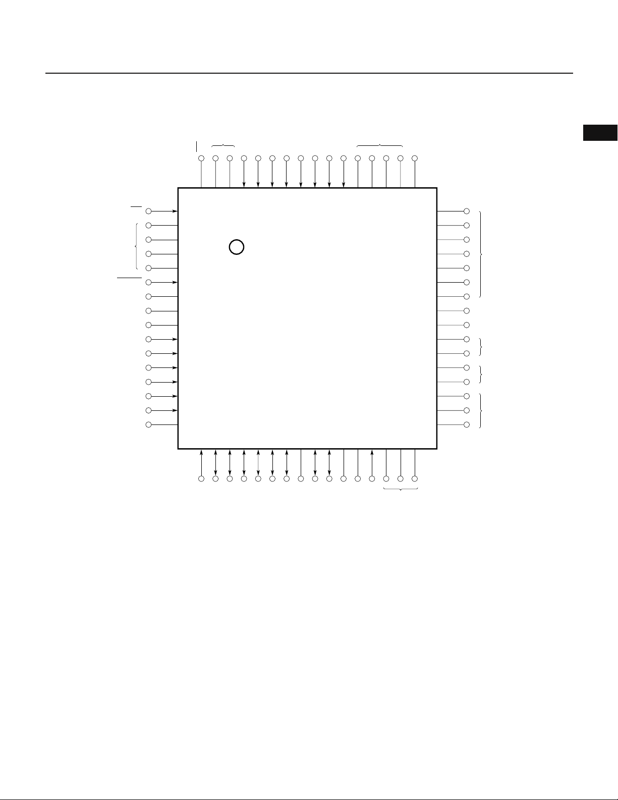
(3) 64-pin plastic QFP (14 × 14 mm)
Chapter 1 General
OE
(L)
RESET
(Open)
(G)
V
A15
A14
A13
A12
A11
A10
(L)
(L)
CE
64 63 62 61 60 59 58 57 56 55 54 53 52 51 50 49
1
2
3
4
5
6
7
8
SS
9
10
11
12
13
14
15
16
A7A6A5A4A3A2A1
µ
µ
µ
PD78P214GC-AB8
PD78P214GC-×××-AB8
PD78P214GC(A)-AB8
A0
(Open)
(L)
48
47
46
45
44
43
42
41
40
39
38
37
36
35
34
33
(L)
VDD
VPP
(L)
(Open)
(G)
1
17 18 19 20 21 22 23 24 25 26 27 28 29 30 31 32
A8
D7D6D5D4D3
Caution The symbols enclosed in parentheses indicate that the corresponding pins, not used in PROM programming mode, shall be handled
as follows:
L : Connect the corresponding pin independently to VSS, through a 10-kΩ resistor.
G : Connect the corresponding pin to VSS.
Open : Leave the corresponding pin unconnected.
D2
SS
D1
D0
V
(Open)
P20/NMI
A9
(G)
★
13
Page 43
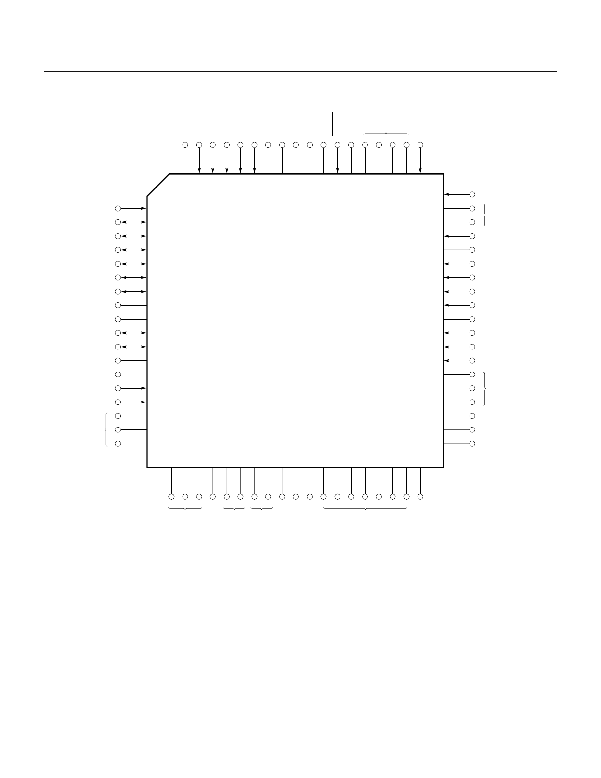
µ
PD78214 Sub-Series
(4) 74-pin plastic QFP (20 × 20 mm)
A8
D7
D6
D5
D4
D3
D2
V
D1
D0
(Open)
NC
P20/NMI
A9
(G)
(L)
A10
A11
A12
A13
A14
(G)
VSSVSS
(G)
(Open)
RESET
NC
74 73 72 71 70 69 68 67 66 65 64 63 62 61 60 59 58 57
1
2
3
4
5
6
7
SS
IC
8
9
10
11
12
13
14
15
16
17
18
µ
µ
PD78P214GJ-5BJ
PD78P214GJ-×××-5BJ
(L)
OE
56
55
54
53
52
51
50
49
48
47
46
45
44
43
42
41
40
39
38
CE
(L)
A7
(Open)
A6
A5
A4
A3
NC
A2
A1
A0
(Open)
NC
(Open)
(L)
19 20 21 22 23 24 25 26 27 28 29 30 31 32 33 34 35 36 37
NC
(G)
(Open)
Caution The symbols enclosed in parentheses indicate that the corresponding pins, not used in PROM programming mode, shall be handled
★
Remark The NC pins are not connected inside the chip.
as follows:
L : Connect the corresponding pin independently to VSS, through a 10-kΩ resistor.
G : Connect the corresponding pin to VSS.
Open : Leave the corresponding pin unconnected.
(L)
VPP
VDD
VDD
(L)
NC
14
Page 44

Chapter 1 General
V
PP
: Programming power supply
RESET : Reset
D0-D7 : Data bus
A0-A14 : Address bus
V
SS
: Ground
OE : Output enable
V
DD
: Power supply
CE : Chip enable
P20/NMI : Port 2/non-maskable interrupt
NC : Non-connection
1
15
Page 45

µ
PD78214 Sub-Series
1.4 EXAMPLE APPLICATION SYSTEM (PRINTER)
PD24C1000
µ
Kanji character
generator
PD78214
µ
Decoder
A16-A19
Pseudo SRAM
PD27C256A
µ
PROM
RD
WR
REFRQ
TO
SCK
SO
Data bus
AD0-AD7
XD
R
TXD
Latch
ASTB
Ports
AVREF
Address bus
A8-A15
AVSS
AN0
AN1
AN2-AN7
Gate array
I/O expansion
Centronics interface, etc.
VSS
VDD
X1 X2
RESET
16
M P00-P03
Stepping motor
Carriage motor
M P04-P07
Paper feed motor
Print head driver
Shift register
RS-232C
driver
Temperature sensor
Motor supply voltage
SW input for each mode
Page 46
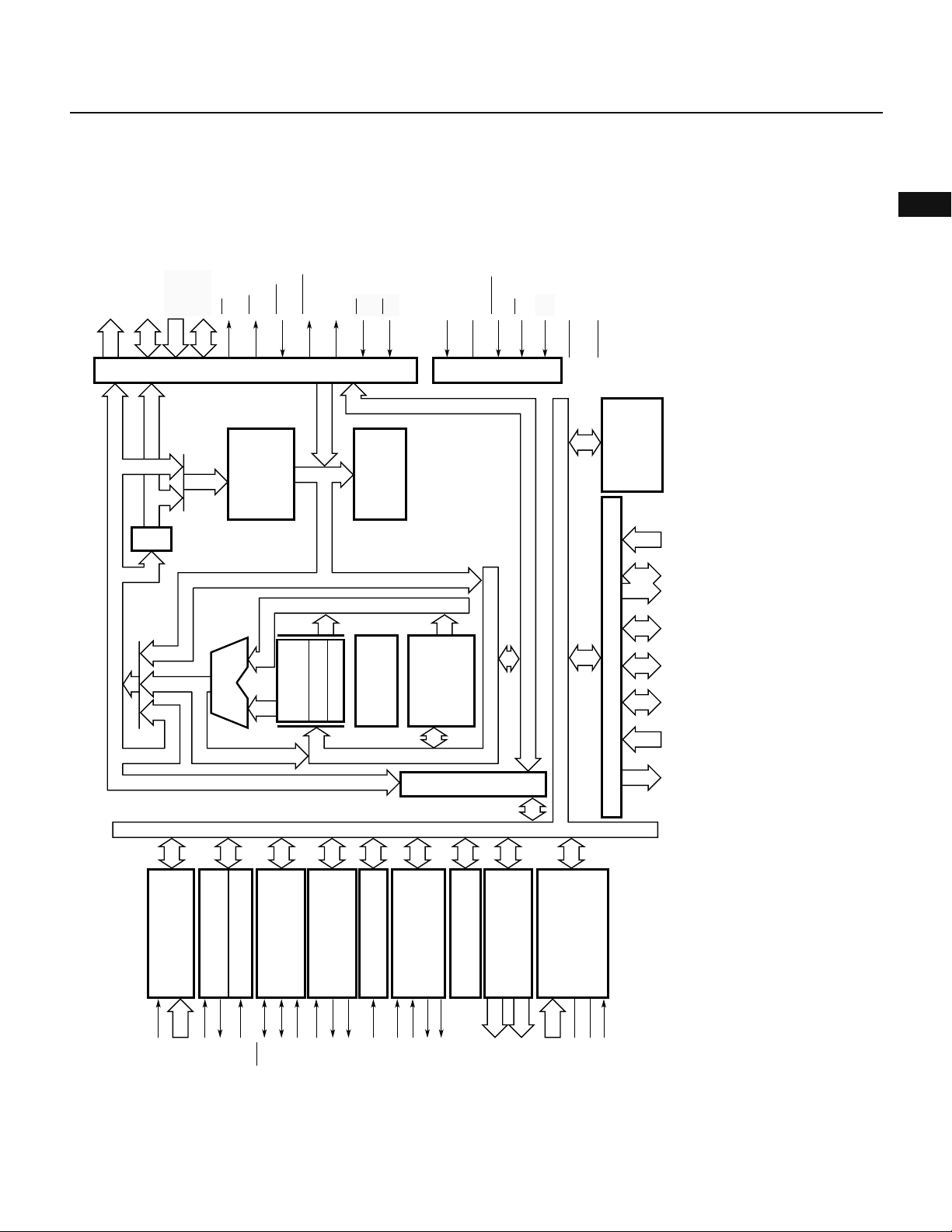
1.5 BLOCK DIAGRAM
A16-A19 (expansion)
A8-A15
AD0-AD7
A0-A14
PC
D0-D7
RD
WR
Note 1
ROM
WAIT
REFRQ
ASTB
CE
OE
• Micro ROM
• Micro-
sequencer
X1
Chapter 1 General
1
X2
RESET
EA
VDD
VPP
System controlBus control
VSS
PD78213(A),
General register
Shaded portions: In PROM
programming mode
GR :
Note 3
RAM
P70
-P75
µ
PD78214(A)
µ
PD78P214,
µ
PD78P214,
µ
PD78214,
µ
PD78214,
µ
PD78213,
µ
Address bus
Programmable
NMI
ALU
UART
interrupt controller
Baud rate generator
TXD
RXD
ASCK
SCK
INTP0-INTP5
Data bus (8)
SP
PSW
Boolean
Temporary
registers
processpr
SFR address/data bus
Timer/counter
Clocked serial interface
Timer/counter (16 bits)
channel-1(PS+8 bits)
SI
TO0
TO1
SO/SB0
INTP3
INTP0
Note 2
• RAM
(256 bytes)
• GR
• Macro service
channel
Bus interface
Timer/counter
channel-2 (PS+8 bits)
Timer/counter
TO2
TO3
INTP1
INTP2
Data bus
channel-3 (PS+8 bits)
Real-time output port
(4 bits×2)
P00-P03
P04-P07
AN0-AN7
Port
A/D converter
AVSS
AVREF
INTP5
P0 P2 P3 P4 P5 P6 P7
P64
P60
P50
P40
P30
P20
P00
-P67
-P63
-P57
-P47
Note 4 Note 4 Note 4
-P37
-P27
-P07
PD78212(A), 16KB for
µ
PD78212(A), 256 bytes for
µ
PD78212 and
µ
PD78212 and
µ
PD78213(A), 8KB for
µ
PD78213 and
µ
PD78213, P40-P47, P50-P57, P64, or P65 do not operate as ports.
µ
PD78214(A)
µ
and
2. Internal dual-port RAM
3. Peripheral RAM (PRAM). 128 bytes for
4. For the
Notes 1. None for
17
Page 47
µ
PD78214 Sub-Series
1.6 FUNCTIONS
Item
Number of basic instructions (mnemonics)
Minimum instruction execution
time (when operating at 12 MHz)
Capacity of
internal memory
Memory area
Number of
I/O pins
Real-time output ports
General-purpose registers
Timer/counters
Input pins
Output pins
I/O pins
Total
Connected to a
pull-up resistor
Driving a LED
directly
Note
Driving a
Special-function
pins
transistor directly
ROM
RAM
µ
PD78212
8K bytes 16K bytes None
384 bytes 512 bytes
64KB for program and 1MB for data
Two four-bit ports or one eight-bit port
Four banks of eight eight-bit registers (memory mapping)
16-bit timer/counter, consisting of
one timer register, one capture
register, and two compare registers.
µ
PD78214
333 ns 500 ns
28 10
54 36
34 16
16 0
µ
PD78P214
65
14
12
8
Pulse output possible (toggle
output or PWM/PPG output)
µ
PD78213
8-bit timer/counter unit 1, consisting of
one timer register, one capture/
compare register, and one compare
register
8-bit timer/counter unit 2, consisting
of one timer register, one capture
register, and two compare registers.
8-bit timer/counter unit 3, consisting
of one timer register and one
compare register
Serial interface
Note The number of I/O pins includes special-function pins.
One-channel UART (special baud rate generator incorporated)
One-channel CSI (three-wire serial I/O, SBI)
Pulse output possible (two
four-bit, real-time outputs)
Pulse output possible (toggle
output or PWM/PPG output)
18
Page 48

Chapter 1 General
A/D converter
Interrupt
Instruction set
Package
Item
µ
µ
PD78212
Eight channels, each having a resolution of eight bits
• 19 interrupts (seven external and 12 internal) plus those caused by
BRK instructions
• Two programmable priority levels
• Two types of interrupt handling, vectored interrupt and macro
service
• 16-bit calculation
• Multiplication (8 bits by 8 bits) and division (16 bits by 8 bits)
• Bit manipulation
• BCD conversion
• Others
• 64-pin plastic shrink DIP (750 mil) for all products
• 64-pin plastic QUIP for all products other than µPD78212,
µ
PD78212(A), and µPD78P214(A)
• 68-pin plastic QFJ for all products other than µPD78212,
µ
PD78212(A), µPD78213(A), and µPD78P214(A)
• 64-pin plastic QFP (14 x 14 mm)
µ
PD78213(A)
• 74-pin plastic QFP (20 x 20 mm) for all products other than
µ
PD78212(A), µPD78213(A), and µPD78P214(A)
• 64-pin ceramic shrink DIP with window (750 mil) for µPD78P214
only
µ
PD78214
µ
PD78P214
Note
for all products other than
PD78213
1
Note Small package with a lead pitch of 0.8 mm, suitable for cameras.
19
Page 49

µ
PD78214 Sub-Series
1.7 DIFFERENCES BETWEEN THE µPD78210
Product
Item
RAM capacity
I/O pins
Timer/counter
Serial interface
Interrupt
A/D converter
Package
Others
128 bytes
• Software programmable pull-up resistors:
Not supported
• Transistor direct drive outputs: Not
supported
PWM/PPG output: Not supported
Scaler for the baud rate generator output:
Not supported
Macro service can be applied to some
interrupt requests.
• Six input pins.
• A voltage ranging from 0 V to AV
applied to the input pins.
64-pin QFP: Not supported
The area at addresses 0FE20H to 0FE7FH can
only be accessed in saddr addressing mode.
µ
PD78210
Note
AND µPD78213
can be
REF
Note For maintenance purposes only.
µ
PD78213
512 bytes
• Software programmable pull-up resistors:
Supported
• Transistor direct drive outputs: Supported
PWM/PPG output: Supported
Scaler for the baud rate generator output:
Supported
Macro service can be applied to all interrupt
requests with the exception of that caused by
a serial receive error.
• Eight input pins.
• A voltage ranging from 0 V to AV
applied only to those pins for which A/D
conversion is being performed, as well as
the pins selected by the ANI0 to ANI3 bits
of the ADM register.
64-pin QFP: Supported
The area at addresses 0FE20H to 0FE7FH can
be accessed in any addressing mode.
REF
can be
20
Page 50

Chapter 1 General
1.8 DIFFERENCES BETWEEN THE µPD78214 SUB-SERIES AND µPD78218A SUB-SERIES
Series name
Product
Minimum instruction cycle
(when operating at 12 MHz)
Operating voltage range
Internal memory
Number of I/O pins 54 36 54 5436
Execution time (number of
clocks) required for PUSH
PSW instruction
One-shot output of 16-bit
timer/counter
Bit width of macro-service
counter
MPD or MPT increment in
macro-service type C
Restriction imposed on data
transfer from memory to SFR
in macro-service type A
Macro-service execution time
Restriction imposed
on input voltage
Restriction imposed
A/D converter
on the AV
Oscillation settling time when
STOP mode is released
Package
ROM
RAM
REF
voltage
µ
(masked ROM)
• Five or seven when internal dual-port RAM is
• Seven or nine in all other cases
Only the eight lower-order bits are incremented.
(The eight high-order bits remain as is.)
The macro-service execution time depends on the macro-service mode and other
factors, and also varies with the sub-series. For details, refer to the table of macroservice execution times in the relevant user's manual.
A voltage ranging from 0 V to AV
applied only to those pins for which A/D conversion is performed and the pins selected by the
ANI0 to ANI3 bits of the ADM register.
Pulse width of NMI at its active level, plus 16
counts on the corresponding counter
• 64-pin plastic shrink DIP (750 mil) for all
• 64-pin plastic QUIP for all products other than
• 68-pin plastic QFJ for all products other than
• 64-pin plastic QFP (14 × 14 mm) for all products
• 74-pin plastic QFP (20 × 20 mm) for all products
• 64-pin ceramic shrink DIP with window (750
µ
PD78214 Sub-Series
µ
µ
PD78212
PD78212(A)
333 ns 500 ns 333 ns 333 ns500 ns
8K bytes
used for the stack area
Transfer data shall not be D0H to DFH.
products
µ
PD78212, µPD78212(A), and µPD78P214(A)
µ
PD78212, µPD78212(A), µPD78213(A), and
µ
PD78P214(A)
other than µPD78213(A)
other than µPD78212(A), µPD78213(A), and
µ
PD78P214(A)
mil) for µPD78P214 only
µ
PD78213
µ
PD78213(A)
ROM-less
3.4 V to V
PD78214
µ
PD78214(A)
16K bytes
(masked ROM)
512 bytes 1024 bytes384 bytes
None
Eight bits
V
= +5 V ±10%
DD
REF
DD
µ
PD78P214
µ
PD78P214(A)
16K bytes
(PROM)
can be
µ
PD78217A
ROM-less
• Six when internal dual-port RAM
is used for the stack area
• Eight in all other cases
Eight bits or 16 bits (selectable,
except for macro service type A)
Transfer source buffer (memory)
addresses shall not be 0FED0H to
0FEDFH.
A voltage ranging from 0 V to
AV
pins for which A/D conversion is
being performed.
15 counts on the corresponding
counter or pulse width of NMI at its
active level, plus 16 counts on the
corresponding counter
• 64-pin plastic shrink DIP (750 mil)
for all products
• 64-pin plastic QFP (14 × 14 mm)
for all products
• 64-pin ceramic shrink DIP with
window (750 mil) for the
µ
PD78P218A only
The 16 bits are incremented.
REF
µ
PD78218A Sub-Series
µ
PD78218A
32K bytes
(masked ROM)
Supported
can be applied only to those
3.6 V to V
DD
µ
PD78P218A
V
= +5 V
DD
±0.3 V
32K bytes
(PROM)
1
21
Page 51

µ
PD78214 Sub-Series
1.9 DIFFERENCES BETWEEN THE µPD78212 AND µPD78212(A)
Product
Item
Quality grade
Package
Standard
• 64-pin plastoc shrink DIP
• 64-pin plastic QFP
• 74-pin plastic QFP
1.10 DIFFERENCES BETWEEN THE
Product
Item
Quality grade
Maximum period in which 74-
pin plastic QFPs can be soldered
satisfactorily, after their sealed
packaging has been opened
Package
Standard
No limit
• 64-pin plastic shrink DIP
• 64-pin plastic QFP
• 74-pin plastic QFP
• 64-pin plastic QUIP
• 68-pin plastic QFJ
µ
PD78212
Special
• 64-pin plastoc shrink DIP
• 64-pin plastic QFP
µ
PD78213 AND µPD78214, AND THE µPD78213(A) AND µPD78214(A)
µ
PD78213, µPD78214
Special
Seven days
Note
Note
Note
µ
PD78212(A)
µ
PD78213(A), µPD78214(A)
Note Not supported for the µPD78213(A)
1.11 DIFFERENCES BETWEEN THE µPD78P214 AND µPD78P214(A)
Item
Quality grade
Package
Product
Standard
• 64-pin plastic shrink DIP
• 64-pin ceramic shrink DIP with window
• 64-pin plastic QFP
• 74-pin plastic QFP
• 64-pin plastic QUIP
• 68-pin plastic QFJ
µ
PD78P214
Special
• 64-pin plastic shrink DIP
• 64-pin plastic QFP
µ
PD78P214(A)
22
Page 52

Chapter 1 General
1.12 DIFFERENCES BETWEEN THE µPD78212, µPD78213, µPD78214, AND µPD78P214
1.12.1 Functional Differences
Product name
Parameter
Internal ROM
Internal RAM
Port 4
Port 5
Port 6
Others
µ
PD78212
8KB masked ROM at
00000H to 01FFFH
384 bytes at 0FD80H
to 0FEFFH
Used as both
general-purpose I/O
port (P40 to P47) and
address/data bus
(AD0 to AD7)
Used as both
general-purpose I/O
port (P50 to P57) and
address bus (A8 to
A15)
P64 and P65 are
used as both
general-purpose I/O
ports, and the RD
and WR pins,
respectively.
———
µ
PD78213
None
512 bytes at 0FD00H to 0FEFFH
Used only as
address/data bus
(AD0 to AD7)
Used only as
address bus (A8 to
A15)
P64 and P65 are
used only as the RD
and WR pins,
respectively.
µ
16KB masked ROM
at 00000H to 03FFFH
Used as both general-purpose I/O port
(P40 to P47) and address/data bus (AD0 to
AD7)
Used as both general-purpose I/O port
(P50 to P57) and address bus (A8 to A15)
P64 and P65 are used as both general-
purpose I/O ports, and the RD and WR
pins, respectively.
PD78214
µ
PD78P214
16KB PROM at
00000H to 03FFFH
PROM programming
mode is supported
1
1.12.2 Package Differences
These products are available with either of two types of QFP (64-pin and 74-pin). Taking differences such as their
soldering conditions, listed below, into consideration, select an appropriate QFP.
Item
Package size
Infrared reflow soldering or
vapor-phase soldering (VPS)
Humidity control for
infrared reflow soldering or
VPS
Soldering conditions
Note The corresponding package is not available for the special quality grade versions of these products, indicated by suffix (A).
14 × 14 mm, lead pitch: 0.8 mm
Supported by µPD78212, µ78213
µ
78214, and µ78P214
The µPD78212, µPD78213
µ
PD78214, and µPD78P214 shall be
soldered within two days of their sealed
package being opened.
64-pin QFP 74-pin QFP
20 × 20 mm, lead pitch: 1.0 mm
Note
,
Supported by µPD78212
Note
µ
Note
78213
,
The µPD78P214
within seven days of its sealed package
being opened.
The µPD78212
µ
PD78214 can be soldered at any time
after their sealed package has been
opened.
, µ78214, and µ78P214
Note
shall be soldered
Note
, µPD78213
Note
,
Note
Note
, and
23
Page 53

24
Page 54

2.1 PIN FUNCTION LIST
CHAPTER 2 PIN FUNCTIONS
2.1.1 Normal Operating mode
(1) Ports
Pin name for
secondary
function
INTP2/CI
INTP4/ASCK
SO/SB0
TO0-TO3
AD0-AD7
A16-A19
WAIT/AN6
REFRQ/AN7
AN0-AN5
Note 1
Note 1
Input/Output
OutputP00-P07
Input
Input/Output
Input/Output
Input/Output
Output
Input/Output
Input
Pin Function
P20
P21
P22
P23
P24
P25
P26
P27
P30
P31
P32
P33
P34-P37
P40-P47
P50-P57
P60-P63
Note 2
P64
Note 2
P65
P66
P67
P70-P75
—
NMI
INTP0
INTP1
INTP3
INTP5
SI
RxD
TxD
SCK
A8-A15
RD
WR
2
Port 0 (P0):
Can be used as two four-bit, real-time output ports. Can drive transistors
directly.
Port 2 (P2):
Cannot be used as a general-purpose port (non-maskable interrupt). The
input level can be checked as part of the interrupt routine. Pins P22 to
P27 can be collectively connected to internal pull-up resistors by means
of software.
Port 3 (P3):
Each pin can be assigned to be either an input or output pin. Input pins
can be collectively connected to internal pull-up resistors by means of
software.
Port 4 (P4):
Can be simultaneously assigned to be either input or output pins. Can be
collectively connected to internal pull-up resistors by means of software.
Can directly drive LEDs.
Port 5 (P5):
Each pin can be assigned to be either an input or output pin. Input pins
can be collectively connected to internal pull-up resistors by means of
software. Can directly drive LEDs.
Port 6 (P6):
Each of pins P64 to P67 can be assigned to be either an input or output
pin. Input pins P64 to P67 can be collectively connected to internal pull-
up resistors by means of software.
Port 7 (P7)
Notes 1. In the case of the µPD78213, these pins do not function as ports.
2. In the case of the µPD78213, neither P64 nor P65 functions as a port.
25
Page 55

µ
PD78214 Sub-Series
(2) Pins other than those which function as ports
Pin Function
TO0-TO3
CI
RxD
TxD
ASCK
SB0
SI
SO
SCK
Input/output
Output
Input
Input
Output
Input
Input/output
Input
Output
Input/output
Timer output
Count clock supplied to eight-bit timer/counter unit 2
Serial data input (UART)
Serial data output (UART)
Baud rate clock input (UART)
Serial data input/output (SB2)
Serial data input (three-wire serial I/O)
Serial data output (three-wire serial I/O)
Serial clock input/output (SBI, three-wire serial I/O)
NMI
INTP0
INTP1
INTP2
Input
External interrupt requests
INTP3
INTP4
INTP5
AD0-AD7
A8-A15
A16-A19
RD
WR
WAIT
ASTB
REFRQ
RESET
X1
X2
Input/output
Output
Output
Output
Output
Input
Output
Output
Input
Input
—
Time-multiplexed address/data bus (external memory connected)
High-order address bus (external memory connected)
High-order address when the addresses are expanded (external memory connected)
Read strobe to external memory
Write strobe to external memory
Wait insertion
Latch timing for addresses A0 to A7 (when external memory is accessed)
Refresh pulse to external pseudo-static memory
Chip reset
Connected to the crystal oscillator used for the system clock (a clock
signal can be input to X1)
Designating ROM-less operation (access to the external memory
EA
Input
mapped to the same area as the internal ROM). Set this pin to low for
the µPD78213, or to high for the µPD78212 and µPD78214.
Pin name for
secondary function
P34-P37
P23/INTP2
P30
P31
P25/INTP4
P33/SO
P27
P33/SB0
P32
P20
P21
P22
P23/CI
P24
P25/ASCK
P26
P40-P47
P50-P57
Note
Note
P60-P63
Note
P64
Note
P65
P66/AN6
—
P67/AN7
—
—
—
AN0-AN5
AN6, AN7
AV
REF
AV
SS
V
DD
V
SS
Input
—
Analog voltage input for A/D converter
A/D converter reference voltage
A/D converter ground
Main power
Ground
NC
Note These pins do not function as ports in the case of the µPD78213.
26
P70-P75
P66/WAIT,
P67/REFRQ
—
—
Page 56

Chapter 2 Pin Functions
2.1.2 PROM Programming Mode (only for the µPD78P214, P20/NMI = 12.5 V, RESET = L)
Pin
P20/NMI
RESET
A0-A14
D0-D7
CE
OE
V
PP
V
DD
V
SS
NC
Input/output
Input
Input/output
Input
—
Setting PROM programming mode
Address bus
Data bus
PROM enable input
Read strobe to PROM
Power for programming
Main power
Ground
Function
—
2.2 PIN FUNCTIONS
2.2.1 Normal Operating mode
(1) P00 to P07 (Port 0): Tristate outputs
Port 0, an eight-bit output port with output latches, can directly drive transistors. Its eight bits can be
simultaneously set to either output mode or high impedance mode by specifying the port-0 mode register
(PM0) accordingly.
Port 0 can output the contents of the buffer registers (P0L, P0H) in real-time at any interval, in units of eight
or four bits (P00 to P03 and P04 to P07). The real-time output port control register (RTPC) determines whether
port 0 is used as a normal output port or real-time output port.
When the RESET signal is input, the output of port 0 becomes high impedance, resulting in the contents of
the output latches becoming undefined.
(2) P20 to P27 (port 2): Inputs
Port 2 is an eight-bit input port. P22 to P27 are provided with software-programmable pull-up resistors. P20
to P27 also act as input pins for control signals such as external interrupts (see Table 2-1). To prevent
malfunctions caused by noise, port 2 provides Schmitt-triggered input circuits.
2
Table 2-1 Port 2 Functions
Port
P20
P21
P22
P23
P24
P25
P26
P27
Note An NMI input is received regardless of whether interrupts are enabled or disabled.
Input port/NMI input
Input port/INTP0 input/CR11 capture trigger input/trigger signal for real-time output port
Input port/INTP1 input/CR22 capture trigger input
Input port/INTP2 input/CI input
Input port/INTP3 input/CR02 capture trigger input
Input port/INTP4 input/ASCK input
Input port/INTP5 input/external trigger signal for A/D converter
Input port/SI input
Note
Function
27
Page 57

µ
PD78214 Sub-Series
(a) When functioning as a port
Signals applied to these pins can be read and these pins can be tested, regardless of whether these pins
are acting as secondary function pins.
(b) When functioning as control-signal input pins
(i) NMI (non-maskable interrupt)
Apply an external non-maskable interrupt request signal to this pin. The external interrupt mode
register (IMTM0) specifies whether an interrupt is detected at its rising or falling edge.
(ii) INTP0 to INTP5 (interrupts from peripherals)
Apply external interrupt request signals to these pins. When an interrupt request signal is detected
at the edge specified by the external interrupt mode registers (INTM0 and INTM1), at any of the INTP0
to INTP5 pins, an interrupt is generated. (For details, see Chapter 11.)
The INTP0 to INTP3 and INTP5 pins can also be used as external trigger input pins for a range of
functions, as described below.
• INTP0: Capture trigger input for eight-bit timer/counter unit 1, and trigger input for real-time output
port
• INTP1: Capture trigger input for eight-bit timer/counter unit 2
• INTP2: External count clock input for eight-bit timer/counter unit 2
• INTP3: Capture trigger input for 16-bit timer/counter
• INTP5: External trigger input for A/D converter
(iii) CI (clock input)
External clock input for eight-bit timer/counter unit 2
(iv) ASCK (asynchronous serial clock)
External baud-rate clock input.
(v) SI (serial input)
Serial data input (when three-wire serial input mode is used)
(3) P30-P37 (port 3): Tristate inputs/outputs
Port 3, an eight-bit input and output port with output latches, is provided with software-programmable pullup resistors. Each pin can be used as an input or output pin by specifying the port-3 mode register (PM3).
It also acts as a control signal pin.
It can be used in either of the following two operating modes, as listed in Table 2-2, by specifying the port3 mode control register (PMC3). The signals applied to these pins can be read and these pins can be tested
regardless of whether these pins are acting as secondary function pins.
When the RESET signal is input, the output of port 3 becomes high impedance, such that it functions as an
input port, resulting in the contents of the output latches becoming undefined.
28
Page 58
Table 2-2 Port 3 Operating Mode (n = 0 to 7)
Chapter 2 Pin Functions
Mode
PMC3 setting
P30
P31
P32
P33
P34
P35
P36
P37
Port mode
PMC3n = 0
I/O port
Control signal I/O mode
PMC3n = 1
RxD input
TxD output
SCK input/output
SO output/SB0 input/output
TO0 output
TO1 output
TO2 output
TO3 output
(a) Port mode
Pins for which port mode is specified by the PMC3 can be used independently as input or output pins by
specifying the port-3 mode register (PM3).
(b) Control signal I/O mode
Each pin can be used as a control signal pin by specifying the PMC3 register.
(i) RxD (receive data)
Serial data input for asynchronous serial interface
(ii) TxD (transmit data)
Serial data output for asynchronous serial interface
(iii) SCK (serial clock)
Serial clock input or output for synchronous serial interface
(iv) SO (serial output)/SBO (serial bus)
Serial data output (when three-wire serial I/O mode is used), or serial bus input or output in SBI mode
(v) TO0 to TO3 (timer output)
Timer outputs
(4) P40-P47 (port 4): Tristate inputs/outputs
Port 4, an eight-bit I/O port with output latches, is provided with software-programmable pull-up resistors and
can directly drive LEDs. Its pins can be collectively used as input or output pins by specifying the memory
expansion mode register (MM).
It acts as a time-multiplexed address/data bus (AD0 to AD7) when external memory or I/O devices are
expanded.
In the case of the µPD78213, it acts as a time-multiplexed address/data bus (AD0 to AD7).
When the RESET signal is input, the output of port 4 becomes high impedance, such that it functions as an
input port, resulting in the contents of the output latches becoming undefined.
(5) P50 to P57 (port 5): Tristate inputs/outputs
Port 5, an eight-bit I/O port with output latches, is provided with software-programmable pull-up resistors and
can directly drive LEDs. Its pins can be used independently as input or output pins by specifying the port-5
mode register(PM5) accordingly.
It acts as an address bus (A8 to A15) when external memory or I/O devices are expanded.
In the case of the µPD78213, it functions as an address bus (A8 to A15).
When the RESET signal is input, the output of port 5 becomes high impedance, such that it functions as an
input port, resulting in the contents of the output latches becoming undefined.
2
29
Page 59
µ
PD78214 Sub-Series
(6) P60 to P67 (port 6): Output (P60 to P63) and tristate inputs/outputs (P64 to P67)
Port 6 is an eight-bit I/O port with output latches. Pins P64 to P67 are provided with software-programmable
pull-up resistors.
The pins of port 6 also function as control signal input pins, as listed in Table 2-3. To use these pins as control
signal input pins, set up is required.
In the case of the µPD78213, P64 and P65 act as an RD output and WR output, respectively.
When the RESET signal is applied, P60 to P63 go low and P64 to P67 function as an input port (the outputs
become high impedance). The contents of the output latches become undefined at the four high-order bits
and 0H at the four low-order bits.
Table 2-3 Port 6 Operating Mode
Pin
P60-P63
P64
P65
P66
P67
Caution While the RESET signal is being applied, P60 to P63 is high impedance. When the RESET signal is released, the output of these pins
is low level. Design the peripheral circuit so that it operates normally when pins P60 to P63 initially output low level.
Remark For details, see Chapter 13.
Port mode Control signal I/O mode
Output port
Input/output
port
A16-A19 output
RD output
WR output
WAIT input/AN6 input
REFRQ output/AN7 input
Operation required to assign pins as control signal pins
Set the MM6 bit of the MM register to 1.
For the µPD78213, specify external memory expansion
mode using bits MM2 to MM0 of the MM register.
Set the PW register, or bits PWn1 and PWn0 (n = 2
and 3) of the MM register and P66 to input mode.
Set the RFEN bit of the RFM register to 1.
(a) Port mode
P60 to P63 are an output port. Each of pins P64 to P67 can be used for input or output by specifying the
port-6 mode register (PM6) accordingly.
(b) Control signal I/O mode
(i) A16 to A19 (address bus)
High-order address bus output when the external memory area is expanded (10000H to FFFFFH). The
memory expansion register (MM) controls these pins.
(ii) RD (read strobe)
Strobe signal output used for reading the external memory. In the case of the µPD78213, the MM
register controls this pin.
(iii) WR (write strobe)
Strobe signal output used for writing to the external memory. In the case of the µPD78213, the MM
register controls this pin.
(iv) WAIT (wait)
Wait signal input. The programmable wait control (PW) register or MM register controls this pin.
(v) REFRQ (refresh request)
Used for outputting refresh pulses to the external pseudo-static memory. The refresh mode register
(RFM) controls this pin.
(vi) AN6 and AN7 (analog input)
Analog inputs to the A/D converter.
(7) P70 to P75 (port 7): Input
Port 7 is a six-bit input port. Its pins also function as analog input pins (AN0 to AN5) for the A/D converter.
Signals applied to these pins can be read and these pins can be tested regardless of whether these pins are
acting as secondary function pins.
30
Page 60

Chapter 2 Pin Functions
(8) ASTB (address strobe): Output
Timing signal output used for latching addresses externally to enable access to external memory.
(9) EA (external access): Input
Control signal input used for switching the program memory from the internal ROM to the external memory.
When this signal is high, the internal ROM is accessed. When low, the external memory is accessed in ROMless mode. In the case of the µPD78212, µPD78214, and µPD78P214, always apply a high-level signal to this
pin. In the case of the µPD78213, apply a low-level signal.
(10) X1 and X2 (crystal)
Pins for connecting the crystal used for internal clock oscillation. When an external clock signal is supplied,
apply it to pin X1. Also, apply the signal having the inverted phase of this clock signal to pin X2.
(11) RESET (reset): Input
Low-active reset input.
(12) AV
(13) AV
(14) V
(15) V
(16) NC (non-connection)
REF
Input of the reference voltage and power for the A/D converter.
SS
A/D converter ground.
DD
Main power input. Connect all VDD pins to the power.
SS
Ground. Connect all VSS pins to the ground.
Not connected inside the chip.
2
2.2.2 PROM Programming Mode (for the µPD78P214)
(1) P20/NMI: Input
Input used for setting the µPD78P214 to PROM programming mode. When a voltage of 12.5 V is applied to
this pin and the RESET pin goes low, the µPD78P214 enters PROM programming mode.
(2) RESET: Input
Input used for setting the µPD78P214 to PROM programming mode. When a low-level signal is applied to this
pin and a voltage of 12.5 V is applied to the P20/NMI pin, the µPD78P214 enters PROM programming mode.
(3) A0 to A14 (address bus): Inputs
Address bus used for the internal PROM (0000H to 3FFFFH). Apply a low-level signal to pin A14.
(4) D0 to D7 (data bus): Inputs/outputs
Data bus, through which programs are read or written to and from the internal PROM.
(5) CE (chip enable): Input
Enable signal input for the internal PROM. When this signal is active, programs can be either written or read.
(6) OE (output enable): Input
Read strobe signal input for the internal PROM. When this input goes active while the CE is low, one byte of
the program at the address specified by pins A0 to A14 in the internal PROM is read through pins D0 to D7.
(7) VPP (programming power supply)
Power supply for writing programs. When the CE goes low while the VPP is 12.5 V and the OE is high, the data
on pins D0 to D7 is written into the internal PROM at the address specified by pins A0 to A14.
(8) V
DD
Main power input.
31
Page 61

µ
PD78214 Sub-Series
(9) V
SS
Ground.
(10) NC (non-connection)
Not connected inside the chip.
32
Page 62
Chapter 2 Pin Functions
2.3 I/O CIRCUITS AND UNUSED-PIN HANDLING
Table 2-4 lists the types of I/O circuits provided for each pin and describes how pins are handled when not used.
Fig. 2-1 illustrates the I/O circuit types.
Pin
P00-P07
P20/NMI
P21/INTP0
P22/INTP1
P23/INTP2/CI
P24/INTP3
P25/INTP4/ASCK
P26/INTP5
P27/SI
P30/RxD
P31/TxD
P32/SCK
P33/SB0/SO
P34/TO0-P37/TO3
P40/AD0-P47/AD7
P50/A8-P57/A15
P60/A16-P63/A19
P64/RD
P65/WR
P66/WAIT/AN6
P67/REFRQ/AN7
P70/AN0-P75/AN5
ASTB
RESET
EA
AV
REF
AV
SS
Table 2-4 Types of I/O Circuits and Unused-Pin Handling
Type of I/O circuit
4 Output
2
2-A
5-A
8-A
10-A
5-A
4
5-A
11
9
4
2
1
—
Input/output Recommended unused-pin handling
Leave open.
Connect to VDD or VSS.
Input
Connect to VDD.
Input/output
Output
Input/output
Input
Output
Input
Connect to VDD when used as an input pin.
Leave open when used as an output pin.
Leave open.
Connect to VDD when used as an input pin.
Leave open when used as an output pin.
Connect to V
Leave open when used as an output pin.
Connect to VSS.
Leave open.
Connect to VDD or V
Connect to VSS.
Note
when used as an input pin.
DD
—
Note
.
SS
2
Note See Section 8.6.
Remark Since the type numbers of I/O circuits are numbered in the 78K series, they may not be serial in a certain product. (A product may
Caution When an I/O pin is used as both an input and output pin, connect the pin to the VDD pin through a resistor of less than 100 kilohms.
not contain some of these I/O circuits.)
(Especially, when the RESET pin goes to a voltage higher than the low level upon power on, or when an I/O pin is switched with
software.)
33
Page 63
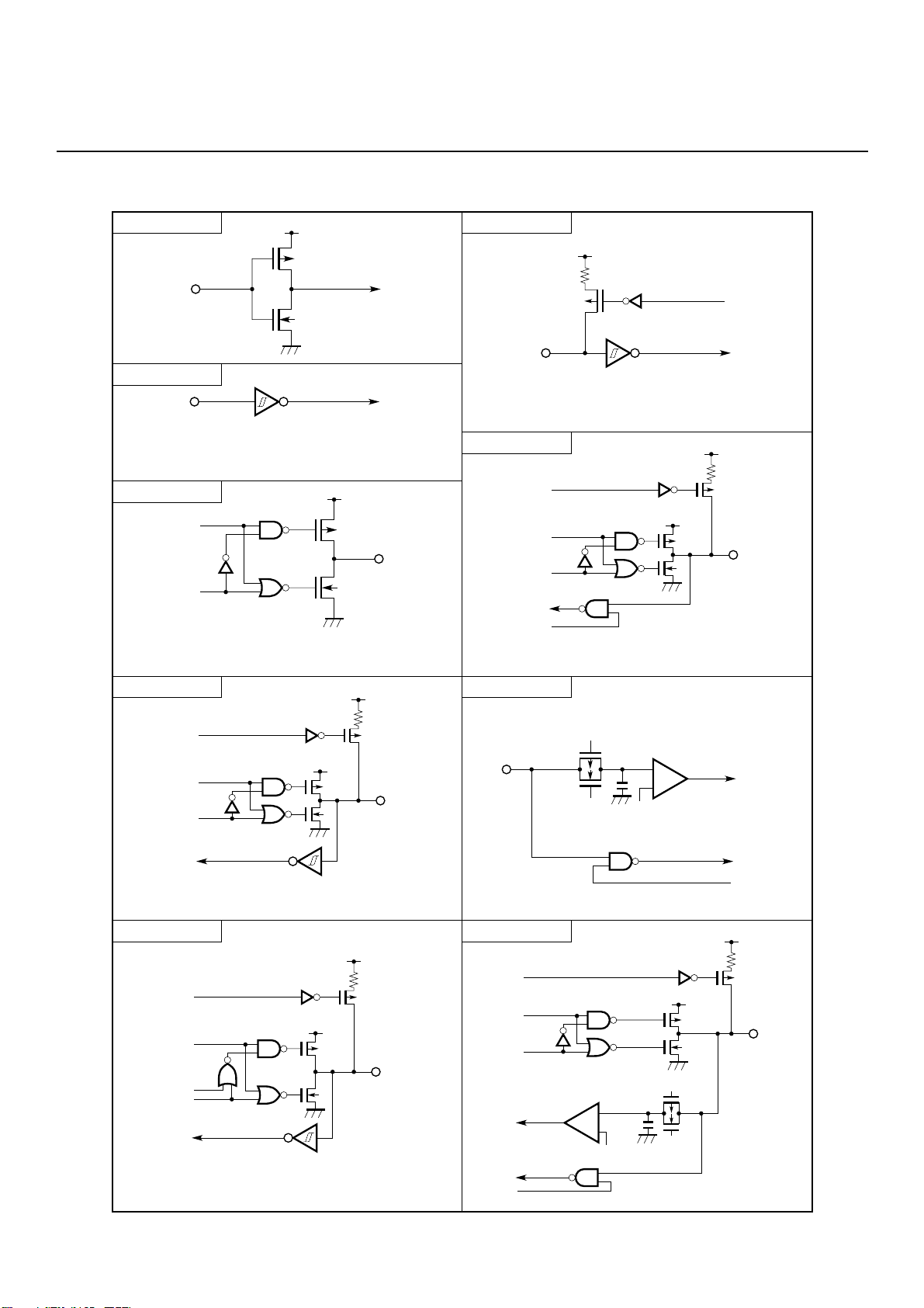
µ
PD78214 Sub-Series
Fig. 2-1 I/O Circuits Provided for Pins
Type 1
V
DD
P
IN
N
Type 2
IN
Schmitt trigger input with hysteresis characteristics
Type 4
Data
Output
disable
DD
V
P
N
Push-pull output which can output high impedance
(both the positive and negative channels are off.)
Type 8-A
V
DD
OUT
Type 2-A
V
DD
P
Pull-up
enable
IN
Schmitt trigger input with hysteresis characteristics
Type 5-A
V
DD
Pull-up
enable
Data
Output
disable
Input
enable
P
V
DD
P
N
Type 9
IN/OUT
Pull-up
enable
Output
disable
Type 10-A
Pull-up
enable
Open
drain
Output
disable
Data
Data
P
Comparator
V
DD
IN
P
P
N
IN/OUT
N
(Threshold voltage)
Vref
+
–
Input
enable
Type 11
V
DD
V
DD
P
V
DD
P
Pull-up
enable
Data
Output
disable
P
V
DD
P
IN/OUT
N
IN/OUT
N
Input
enable
Comparator
+
–
Vref
(Threshold voltage)
P
N
34
Page 64

Chapter 2 Pin Functions
2.4 NOTES
(1) While the RESET signal is being applied, pins P60 to P63 are high impedance. When the RESET signal is
released, the output of these pins is low level. Design the peripheral circuit so that it operates satisfactorily
when pins P60 to P63 initially output the low level.
(2) When an I/O pin is used as both an input and output pin, connect the pin to the VDD pin through a resistor of
less than 100 kilohms. (Especially, when the RESET pin goes to a voltage higher than the low level upon power
on, or when an I/O pin is switched with software.)
2
35
Page 65

36
Page 66

CHAPTER 3 CPU FUNCTION
3.1 MEMORY SPACE
The µPD78214 can access a memory space of up to 1M byte. Figs. 3-1 to 3-4 show the corresponding memory
maps. The mapping of program memory depends on the status of the EA pin. The EA pin of the µPD78213 must
be tied low.
(1)µPD78212
Program memory is mapped to the internal ROM (8K bytes: 00000H to 01FFFH) and external memory (56704
bytes: 02000H to 0FD7FH). External memory is accessed in external memory expansion mode. The area
mapped as external memory can also be used as data memory.
Data memory is mapped to internal RAM (384 bytes: 0FD80H to 0FEFFH). In 1M-byte expansion mode,
external memory (960K bytes: 10000H to FFFFFH) is mapped as expanded data memory.
(2)µPD78213
Program memory is mapped to external memory (64768 bytes: 00000H to 0FCFFH). This area can also be used
as data memory.
Data memory is mapped to internal RAM (512 bytes: 0FD00H to 0FEFFH). In 1M-byte expansion mode,
external memory (960K bytes: 10000H to FFFFFH) is mapped as expanded data memory.
(3)µPD78214, µPD78P214
Program memory is mapped to internal ROM (16K bytes: 00000H to 03FFFH) and external memory (48384
bytes: 04000H to 0FCFFH). External memory is accessed in external memory expansion mode. The area
mapped as external memory can also be used as data memory.
Data memory is mapped to internal RAM (512 bytes: 0FD00H to 0FEFFH). In 1M-byte expansion mode,
external memory (960K bytes: 10000H to FFFFFH) is mapped as expanded data memory.
3
37
Page 67

µ
PD78214 Sub-Series
Fig. 3-1 Memory Map of µPD78212 (EA Pin Driven High)
FFFFFH
Data memory
Expansion address
10000H
0FFFFH
0FFDFH
0FFD0H
0FF00H
0FEFFH
Data
memory
0FD80H
0FD7FH
Memory space (1M byte)
Program memory/
data memory
02000H
01FFFH
Program memory/
data memory
00000H
External memory
(960K bytes)
Special function registers (SFR)
Note 2
(256 bytes)
Internal RAM
(384 bytes)
External memory
(56704 bytes)
Internal ROM
(8K bytes)
Note 1
0FEFFH
0FEE0H
0FEDFH
0FEC2H
0FD80H
01FFFH
01000H
00FFFH
00800H
007FFH
00080H
0007FH
00040H
0003FH
00000H
General registers
(32 bytes)
Macro service control
words (30 bytes)
Data area
(512 bytes)
Program area
(4K bytes)
CALLF entry area
(2K bytes)
Program area
(1920 bytes)
CALLT table area
(64 bytes)
Vector table area
(64 bytes)
Notes 1. Accessed in 1M-byte expansion mode.
2. External SFR area
Remark The shaded areas indicate internal memory.
38
Page 68

Fig. 3-2 Memory Map of µPD78212 (EA Pin Driven Low)
FFFFFH
Chapter 3 CPU Function
Data memory
Expansion address
10000H
0FFFFH
0FFDFH
0FFD0H
0FF00H
0FEFFH
Data
memory
0FD80H
0FD7FH
Memory space (1M byte)
Ordinary address (64K bytes)
Program memory/data memory
00000H
External memory
(960K bytes)
Special function registers (SFR)
Note 2
(256 bytes)
Internal RAM
(384 bytes)
External memory
(64896 bytes)
Note 1
0FEFFH
0FEE0H
0FEDFH
0FEC2H
0FD80H
00FFFH
00800H
007FFH
00080H
0007FH
00040H
0003FH
00000H
3
General registers
(32 bytes)
Macro service control
words (30 bytes)
Data area
(512 bytes)
CALLF entry area
(2K bytes)
Program area
(1920 bytes)
CALLT table area
(64 bytes)
Vector table area
(64 bytes)
Notes 1. Accessed in 1M-byte expansion mode.
2. External SFR area
Remark The shaded areas indicate internal memory.
39
Page 69

µ
PD78214 Sub-Series
Fig. 3-3 Memory Map of µPD78213, µPD78214, or µPD78P214 (EA Pin Driven Low)
FFFFFH
Data memory
Expansion address
10000H
0FFFFH
0FFDFH
0FFD0H
0FF00H
0FEFFH
Data
memory
0FD00H
0FCFFH
Memory space (1M byte)
Ordinary address (64K bytes)
Program memory/data memory
00000H
External memory
(960K bytes)
Special function registers (SFR)
Note 2
(256 bytes)
Internal RAM
(512 bytes)
External memory
(64768 bytes)
Note 1
0FEFFH
0FEE0H
0FEDFH
0FEC2H
0FD00H
00FFFH
00800H
007FFH
00080H
0007FH
00040H
0003FH
00000H
General registers
(32 bytes)
Macro service control
words (30 bytes)
Data area
(512 bytes)
CALLF entry area
(2K bytes)
Program area
(1920 bytes)
CALLT table area
(64 bytes)
Vector table area
(64 bytes)
Notes 1. Accessed in 1M-byte expansion mode.
2. External SFR area
Remark The shaded areas indicate internal memory.
40
Page 70

Chapter 3 CPU Function
Fig. 3-4 Memory Map of µPD78214, µPD78P214 (EA Pin Driven High)
FFFFFH
Data memory
Expansion address
10000H
0FFFFH
0FFDFH
0FFD0H
0FF00H
0FEFFH
Data
memory
0FD00H
0FCFFH
Memory space (1M byte)
Program memory/
data memory
Ordinary address (64K bytes)
04000H
03FFFH
Program memory/
data memory
00000H
External memory
(960K bytes)
Special function registers (SFR)
Notes 2, 3
(256 bytes)
Internal RAM
(512 bytes)
External memory
(48384 bytes)
Internal ROM
(16K bytes)
Note 1
0FEFFH
0FEE0H
0FEDFH
0FEC2H
0FD00H
03FFFH
01000H
00FFFH
00800H
007FFH
00080H
0007FH
00040H
0003FH
00000H
3
General registers
(32 bytes)
Macro service control
words (30 bytes)
Data area
(512 bytes)
Program area
(12K bytes)
CALLF entry area
(2K bytes)
Program area
(1920 bytes)
CALLT table area
(64 bytes)
Vector table area
(64 bytes)
Notes 1. Accessed in 1M-byte expansion mode.
2. Accessed in external memory expansion mode
3. External SFR area
Remark The shaded areas indicate internal memory.
41
Page 71

µ
PD78214 Sub-Series
3.1.1 Internal Program Memory Area
In the area from 00000H to 03FFFH (00000H to 01FFFH for the µPD78212), a 16K × 8 bit ROM (8K × 8 bit ROM for
the µPD78212) is incorporated. Programs and table data are stored in this area. Usually, the program counter (PC)
is used for addressing.
If the µPD78213 is used or if the EA pin is driven low, this area becomes external memory (ROM-less operation).
(1) Vector table area
The 64-byte area from 00000H to 0003FH is reserved as a vector table area. Stored in the vector table area
is the program start address to which a program is branched if RESET is input or if an interrupt request occurs.
The low-order eight bits of the 16-bit address are stored at even-numbered addresses, and the high-order
eight bits at odd-numbered addresses.
Table 3-1 Vector Table
Vector table address
00000H
00002H
00006H
00008H
0000AH
0000CH
0000EH
00010H
00012H
00014H
00016H
00018H
0001AH
0001CH
00020H
00022H
00024H
00026H
0003EH
Interrupt request
Reset (RESET input)
NMI
INTP0
INTP1
INTP2
INTP3
INTP4/INTC30
INTP5/INTAD
INTC20
INTC00
INTC01
INTC10
INTC11
INTC21
INTSER
INTSR
INTST
INTCSI
BRK
(2) CALLT instruction table area
In the 64-byte area from 00040H to 0007FH, the subroutine entry address of a one-byte call instruction (CALLT)
can be stored.
(3) CALLF instruction entry area
A two-byte call instruction (CALLF) can directly call a subroutine, starting from an address between 00800H
and 00FFFH.
42
Page 72

Chapter 3 CPU Function
3.1.2 Internal RAM Area
A 512-byte (384-byte for the µPD78212) general-purpose static RAM is incorporated into the area from 0FD00H to
0FEFFH.
This area consists of the following two RAMs:
Peripheral RAM (PRAM) : 0FD00H to 0FDFFH (0FD80H to 0FDFFH for the µPD78212)
°
Internal dual-port RAM (IRAM): 0FE00H to 0FEFFH
°
The internal dual-port RAM (IRAM) can be accessed at high speed.
Short direct addressing mode for high-speed access can be used for the area from 0FE20H to 0FEFFH. (Refer to
Chapter 6, Instruction, “78K/II Series User’s Manual.”)
General-purpose registers of four banks are mapped into the 32-byte area from 0FEE0H to 0FEFFH. Macro service
control words are mapped into the 30-byte area from 0FEC2H to 0FEDFH.
Caution Program fetch from the internal RAM area is prohibited.
Remark It is convenient to store data, work areas, and status flags that are frequently accessed in the area from 0FE20H to 0FEC1H. The area
from 0FE00H to 0FE1FH can be accessed at high speed. If this area is used as a stack area, macro service channel, or a data transfer
area for a macro service, system throughput can be improved. (For this area, short direct addressing cannot be used. This area is
addressed in the same way as other memory spaces. The area, however, can be accessed faster than other memory spaces. In terms
of the efficiency of the entire system, it is advantageous to use the area as a stack area, macro service channel, or a data transfer area
for a macro service channel.)
3
3.1.3 Special Function Register (SFR) Area
Special function registers (SFR), which are on-chip hardware peripherals, are mapped into the area from 0FF00H
to 0FFFFH (see Section 3.2.5).
The area from 0FFD0H to 0FFDFH is mapped as an external SFR area. This area allows the µPD78214 in external
memory expansion mode (selected by memory expansion mode register MM) and µPD78213 (ROM-less) to access
external peripheral I/O.
Caution Never access an address to which no SFR is mapped in this area. If this is attempted, the µPD78214 may enter a deadlock. To restore
the device from the deadlock, a reset signal must be input.
3.1.4 External SFR Area
In the SFR area, the 16-byte area from 0FFD0H to 0FFDFH is mapped as an external SFR area. This area allows the
µ
PD78214 in external memory expansion mode (selected by memory expansion mode register MM) and the
µ
PD78213 (ROM-less) to access external peripheral I/O through the address bus or address/data bus.
The external SFR area can be accessed by the SFR addressing method. The area features the following: Peripheral
I/O can be easily manipulated and the object size can be compressed. This area can also be specified as an SFR
of macro service type B.
When the external SFR area is accessed, the bus operates as in ordinary memory access (see Chapter 13).
3.1.5 External Memory Space
The area from 04000H to 0FCFFH (02000H to 0FD7FH for the µPD78212) is an external memory space that can be
accessed by setting a memory expansion mode register (MM). In this area, programs and table data can be stored
and peripheral I/O devices can be mapped.
For the µPD78213, the area from 00000H to 0FCFFH can be accessed at any time.
3.1.6 External Extension Data Memory Space
The area from 10000H to FFFFFH can be accessed if 1M-byte expansion mode is selected by the memory expansion
mode register (MM). In this mode, pins P60 to P63 of port 6 function as the expansion address bus of four bits (A16
to A19). The data memory space is manipulated as 16 banks of 64K bytes. The low-order four bits of registers P6
and PM6 function as a bank register for selecting a bank. This memory space is useful if the kanji character
generator or a large amount of data is used.
43
Page 73

µ
PD78214 Sub-Series
To access the space, specify the bank to be used (high-order four bits of address, A16 to A19) in the bank register
(P60 to P63 of register P6, or PM60 to PM63 of register PM6). Then, execute an instruction which allows extended
addressing. The high-order four bits of address output from pins P60 to P63 are valid only while an instruction
that allows extended addressing is being executed.
Because two bank registers are provided, two data banks can always be used. To select either of the two bank
registers, specify the operand of the instruction with or without &. If & is added, register P6 is selected as the bank
register. If & is omitted, register PM6 is selected as the bank register.
If one of the two banks is specified as the main data bank in a RAM area, and if the other bank is specified as the
sub-data bank in a data ROM area, for example, the data read from the data ROM (for example, character data for
the printer) can easily be enlarged or reduced in size and stored in the RAM.
Example Specifying bank 1 as the main bank and bank 5 as the sub-bank and transferring the data from bank 5 to bank 1
MOV MM, #47H ; Selects memory expansion mode.
MOV PM6, #1H ; Sets the main bank register (PM6).
MOV P6, #5H ; Sets the sub-bank register (P6).
MOV B, #0FFH ; Sets the loop counter.
·
·
·
LOOP :
·
·
·
·
·
MOV A, &[HL+] ; Reads data from bank 5. (The contents of register P6 are added as the most significant address.)
MOV [DE+], A ; Stores the data in bank 1. (The contents of register PM6 are added as the most significant address.)
·
·
·
·
·
·
·
DBNZ B, $LOOP ; Repetition
Fig. 3-5 Sample Data Transfer between Banks
Bank 1
10000H
1FFFFH
Remarks 1. The MOV [DE+], A and MOV A, &[HL+] instructions are both held in bank 0.
2. The instruction that uses register PM6 as the bank register requires a shorter instruction code and shorter execution time than
that which uses register P6. The instruction that manipulates register P6 requires a shorter instruction code and shorter execution
time than that which manipulates register PM6. It is, therefore, efficient to use PM6 as the main bank register that specifies the
bank accessed most frequently and P6 as the sub-bank register that frequently specifies different banks.
(main data bank)
50000H
5FFFFH
MOV [DE+], A MOV A, &[HL+]
A register
Bank 5
(auxiliary data bank)
44
Page 74

Chapter 3 CPU Function
3.2 REGISTERS
3.2.1 Program Counter (PC)
This 16-bit binary counter holds the address of the program to be executed next (see Fig. 3-6).
Usually, the address is automatically incremented according to the number of bytes of the instruction to be
fetched. If an instruction causing a branch is executed, the contents of the register or immediate data are set.
µ
When RESET is input, the contents at address 00000H of the internal ROM (external memory for the
are specified in the low-order eight bits of the PC and the contents at address 00001H are specified in the high-order
eight bits of the PC.
Fig. 3-6 Configuration of the Program Counter
1514131211109876543210
PC15 PC14 PC13 PC12 PC11 PC10 PC9 PC8 PC7 PC6 PC5 PC4 PC3 PC2 PC1 PC0
PC
3.2.2 Program Status Word (PSW)
This 8-bit register consists of flags that are set or reset according to the execution results of an instruction (see Fig.
3-7).
The contents can be read and written in units of eight bits. Each flag can be manipulated by a bit manipulation
instruction. The PSW is saved to a stack when a vectored interrupt request is acknowledged or when the BRK or
PUSH PSW instruction is executed. The PSW is restored when an RETI, RETB, or POP PSW instruction is executed.
When RESET is input, the PSW is set to 02H. (In this state, no interrupt requests can be acknowledged.)
PD78213)
3
Fig. 3-7 Configuration of the Program Status Word
76543210
IE Z RBS1 AC RBS0 0 ISP CY
PSW
(1) Carry flag (CY)
This flag indicates whether an overflow or underflow occurs when an add/subtract instruction is executed.
If a shift/rotate instruction is executed, the flag holds a shift-out value. If a bit arithmetic/logical instruction
is executed, the flag functions as a bit accumulator.
(2) Interrupt priority status flag (ISP)
This flag manages the priority of maskable vectored interrupts that can currently be acknowledged. If a
maskable interrupt is acknowledged, the contents of the priority designation flag of the acknowledged
interrupt are transferred to the ISP flag. If a non-maskable interrupt (NMI) is acknowledged, this flag is set to
0.
If the ISP flag is set to 0, vectored interrupts assigned a lower priority by the priority designation flag register
(PR0) cannot be acknowledged. If the ISP flag is set to 1, interrupts can be acknowledged, independent of the
priority. The actual acknowledgment of interrupts is controlled according to the status of the IE flag.
The contents are updated each time a maskable vectored interrupt is acknowledged.
For details, see Chapter 12.
45
Page 75
µ
PD78214 Sub-Series
(3) Register bank selection flags (RBS0, RBS1)
These two flags are used to select one of four register banks (see Table 3-2).
The flags hold two-bit information indicating the register bank selected by the SEL RBn instruction.
Table 3-2 Selecting a Register Bank
RBS1
0
0
1
1
RBS0 Specified register bank
0
1
0
1
Register bank 0
Register bank 1
Register bank 2
Register bank 3
(4) Auxiliary carry flag (AC)
If an operation generates a carry from bit 3 or a borrow into bit 3, this flag is set (1). Otherwise, the flag is reset
(0).
The flag is used when a BCD conversion instruction is executed.
(5) Zero flag (Z)
If an operation results in zero, this flag is set (1). Otherwise, the flag is reset (0).
(6) Interrupt request enable flag (IE)
This flag controls the CPU’s acknowledgment of interrupt requests.
If the flag is set to 0, interrupts are inhibited. Only nonmaskable interrupts and unmasked macro services can
be acknowledged. All other interrupts are prohibited.
If the flag is set to 1, interrupts are permitted. The ISP flag, interrupt mask flag corresponding to each interrupt
request, and priority designation flag control the acknowledgment of an interrupt request.
When the EI instruction is executed, the IE flag is set (1). When the DI instruction is executed or when an
interrupt is acknowledged, the flag is reset (0).
3.2.3 Stack Pointer (SP)
This 16-bit register holds the first address of a stack area (LIFO: 00000H to 0FFFFH) (see Fig. 3-8). The stack pointer
is used to address a stack area when a subroutine is executed or when an interrupt is handled.
The contents of the SP are decremented before data is written into the stack area and incremented after data is
read from the stack area (see Figs. 3-9 and 3-10).
A special instruction can access the SP.
The contents of the SP become undefined when RESET is input. Immediately after a reset is released (before a
subroutine is called or before an interrupt is acknowledged), run an initialization program to initialize the SP.
Example Initializing the SP
MOVW SP, #0FEE0H; SP ← 0FEE0H (if used from FEDFH)
Fig. 3-8 Configuration of the Stack Pointer
0
SP1515SP1414SP1313SP1212SP1111SP1010SP99SP88SP77SP66SP55SP44SP33SP22SP11SP0
SP
46
Page 76

Fig. 3-9 Data Saved to the Stack Area
Chapter 3 CPU Function
SP ← SP – 2
SP – 2
↑
SP – 1
↑
SP ⇒
PUSH rp instruction
Stack
Register pair, low
Register pair, high
CALL, CALLF, and CALLT instructions
SP ← SP – 2
SP – 2
↑
SP – 1
↑
SP ⇒
Stack
PC7-PC0
PC15-PC8
SP ← SP – 3
SP – 3
↑
SP – 2
↑
SP – 1
↑
SP ⇒
Interrupt
Stack
PC7-PC0
PC15-PC8
PSW
Fig. 3-10 Data Restored from the Stack Area
POP rp instruction
Stack
Register pair, low
SP ⇒
↓
SP + 1
SP + 2
SP ← SP + 2
Cautions 1. In stack addressing, the entire 64K bytes can be accessed. A stack area cannot be mapped in the SFR area or internal ROM area.
2. The SP becomes undefined when RESET is input. Meanwhile, nonmaskable interrupts can be acknowledged immediately after
a reset is released. If a nonmaskable interrupt request occurs, while the SP is undefined, immediately after a reset is released,
an unpredictable operation may be carried out. To minimize this danger, initialize the SP immediately after a reset is released.
For details, see Section 12.3.2.
Register pair, high
↓
SP ⇒
↓
SP + 1
↓
SP + 2
SP ← SP + 2
RET instruction
Stack
PC7-PC0
PC15-PC8
SP ⇒
↓
SP + 1
↓
SP + 2
↓
SP + 3
SP ← SP + 3
RETI instruction
Stack
PC7-PC0
PC15-PC8
PSW
3
3.2.4 General-Purpose Registers
(1) Configuration
General-purpose registers are mapped to special addresses (0FEE0H to 0FEFFH) in data memory. The
registers are grouped into four banks, each of which consists of eight 8-bit registers (X, A, C, B, E, D, L, H) (see
Fig. 3-11).
47
Page 77
µ
PD78214 Sub-Series
0FEE0H
0FEFFH
Fig. 3-11 Configuration of General-Purpose Registers
(8-bit processing) (16-bit processing)
A E1H
B E3H
D E5H
H E7H
A E9H
B EBH
D EDH
H EFH
A F1H
B F3H
D F5H
H F7H
A F9H
B FBH
D FDH
H FFH
X E0H
C E2H
E E4H
L E6H
X E8H
C EAH
E ECH
L EEH
X F0H
C F2H
E F4H
L F6H
X F8H
C FAH
E FCH
L FEH
↑
Register bank 3
(RBS1, 0 = 11)
↓
↑
Register bank 2
(RBS1, 0 = 10)
↓
↑
Register bank 1
(RBS1, 0 = 01)
↓
↑
Register bank 0
(RBS1, 0 = 00)
↓
AX
BC
DE
HL
AX
BC
DE
HL
AX
BC
DE
HL
AX
BC
DE
HL
E0H
E2H
E4H
E6H
E8H
EAH
ECH
EEH
F0H
F2H
F4H
F6H
F8H
FAH
FCH
FEH
To specify the register bank to be used to execute an instruction, use the CPU control instruction (SEL RBn).
When RESET is input, register bank 0 is specified.
The current register bank can be checked by reading the register bank selection flags (RBS0, RBS1) in the PSW.
The area from 0FEE0H to 0FEFFH can be addressed and accessed as an ordinary data memory area,
irrespective of whether the area is used for general-purpose registers.
Remark To restore the current register bank after it is changed to a different register bank, execute the PUSH PSW instruction to save the PSW
to a stack, then execute the SEL RBn instruction. The POP PSW instruction can restore the register bank if the stack position is not
changed. If an interrupt handling program changes the register bank, the PSW is automatically saved to a stack when an interrupt
is acknowledged. The PSW is restored by the RETI or RETB instruction. If a single register bank is predetermined for the interrupt
handling routine, only the SEL RBn instruction need be executed. The PUSH PSW instruction need not be executed.
Examples 1. Changing the register bank by an ordinary program
Specifying register bank 2
·
·
·
·
·
PUSH PSW
SEL RB2
·
·
·
·
·
POP PSW
·
·
·
·
·
Register bank 2 is used.
The previous register bank is used.
2. Changing the register bank by an interrupt handling program
Selecting register bank 1
SEL RB1
·
·
·
·
·
RETI
Register bank 1 is used.
The previous register bank is automatically
restored upon return from the interrupt
handling program.
48
Page 78

Chapter 3 CPU Function
(2) Function
General-purpose registers can be operated in units of eight bits. They can also be operated in units of 16 bits,
that is, a pair of eight-bit registers can be operated as a single unit (AX, BC, DE, HL).
Each register can temporarily hold operation results or can be used as an operand of an arithmetic/logical
instruction between registers.
General-purpose registers are grouped into four register banks. By separating the register banks to be used
for ordinary operation from those for interrupt handling, an efficient program can be created.
The registers have different functions as described below:
A (R1) : Central register for the transfer of 8-bit data or arithmetic/logical operations. This
register can also hold bit data.
The register can also hold the offset value for indexed addressing.
AX (RP0) : Central register for the transfer of 16-bit data or arithmetic/logical operations
X (R0) : Register that can hold bit data
B (R3) : Register with the functions of a loop counter. The register can be used by the DBNZ
instruction.
This register can also hold the offset value for indexed addressing.
C (R2) : Register with the functions of a loop counter. The register can be used by the DBNZ
instruction.
DE (RP2), HL (RP3) : Registers with the functions of a pointer. The registers specify a base address for register
indirect addressing and base addressing.
This register can also hold the offset value for indexed addressing.
Each register can be identified by a name representing its function (X, A, C, B, E, D, L, H, AX, BC, DE, HL) or
by an absolute name (R0 to R7, RP0 to RP3). For details of the relationship between the function names and
absolute names, see Table 3-3.
3
Table 3-3 Function Names and Absolute Names
Function name Absolute name
X
A
C
B
E
D
L
H
R0
R1
R2
R3
R4
R5
R6
R7
Function name Absolute name
AX
BC
DE
HL
RP0
RP1
RP2
RP3
49
Page 79

µ
PD78214 Sub-Series
3.2.5 Special Function Registers (SFR)
A mode register, control register, and other registers with special functions, which are built-in hardware
peripherals, are mapped into the 256-byte space from 0FF00H to 0FFFFH.
Caution Never access an address to which no SFR is mapped in this area. If this is attempted, the µPD78214 may enter a deadlock. To clear
Table 3-4 lists the special function registers (SFR). The following column headings are used:
• Symbol : Symbol indicating the built-in SFR. This is a reserved word for NEC’s assembler (RA78K/II). For the
• R/W : Whether the contents of the SFR can be read or written
• Bit unit : Number of bits that can be manipulated when the SFR is operated. The SFR that can be manipulated
• At reset : Status of the register when RESET is input
the deadlock, a reset signal must be input to the device.
C compiler (CC78K/II), the #pragma sfr instruction allows this symbol to be used as an sfr variable.
R/W : Read/write
R : Read-only
W : Write-only
in units of 16 bits can be coded in the sfrp operand or specified by an even address. The SFR that can
be manipulated in one-bit units can be coded in the bit manipulation instruction.
50
Page 80

Table 3-4 Special Function Registers (SFR) (1/2)
Chapter 3 CPU Function
Address
0FF00H
0FF02H
0FF03H
0FF04H
0FF05H
0FF06H
0FF07H
0FF0AH
0FF0BH
0FF0CH
0FF10H
0FF11H
0FF12H
0FF13H
0FF14H
0FF15H
0FF16H
0FF17H
0FF18H
0FF19H
0FF1AH
0FF1CH
0FF20H
0FF23H
0FF25H
0FF26H
0FF30H
0FF31H
0FF32H
0FF34H
0FF40H
0FF43H
Port 0
Port 2
Port 3
Port 4
Port 5
Port 6
Port 7
Port 0 buffer register
Port 0 buffer register
Real-time output port control register
16-bit compare register 0
(16-bit timer/counter)
16-bit compare register 1
(16-bit timer/counter)
8-bit compare register
(8-bit timer/counter 1)
8-bit compare register
(8-bit timer/counter 2)
8-bit compare register
(8-bit timer/counter 2)
8-bit compare register
(8-bit timer/counter 3)
16-bit capture register
(16-bit timer/counter)
8-bit capture register
(8-bit timer/counter 2)
8-bit capture/compare register
(8-bit timer/counter 1)
Port 0 mode register
Port 3 mode register
Port 5 mode register
Port 6 mode register
Capture/compare control register 0
Timer output control register
Capture/compare control register 1
Capture/compare control register 2
Pull-up-resistor-option register
Port 3 mode control register
Symbol
P0
P2
P3
P4
P5
P6
P7
P0L
P0H
RTPC
CR00
CR01
CR10
CR20
CR21
CR30
CR02
CR22
CR11
PM0
PM3
PM5
PM6
CRC0
TOC
CRC1
CRC2
PUO
PMC3
R/W
R
R/W
R
R/W
R
R/W
W
R/W
W
R/W
Bit unit
16 bits8 bits1 bit
°
°
°
°
°
°
°
°
°
°
—
—
—
—
—
—
—
—
—
—
—
—
—
—
—
—
—
—
—
—
—
°
—
—
—
—
°
°
—
°
—
°
—
°
°
—
°
°
—
°
°
—
°
—
°
°
°
°
—
°
°
—
°
°
—
°
—
°
—
°
—
°
—
°
—
°
°
—
°
—
°
—
°
—
°
—
°
At resetName of special function register (SFR) R/W
3
Not defined
×0H
Not defined
00H
Not defined
FFH
F×H
10H
00H
51
Page 81

µ
PD78214 Sub-Series
Table 3-4 Special Function Registers (SFR) (2/2)
0FF50H
0FF51H
0FF52H
0FF54H
0FF56H
0FF5CH
0FF5DH
0FF5EH
0FF5FH
0FF68H
0FF6AH
0FF80H
0FF82H
0FF86H
0FF88H
0FF8AH
0FF8CH
0FF8EH
0FF90H
0FFC0H
0FFC4H
0FFC5H
0FFC6H
0FFD0H
0FFDFH
0FFE0H
0FFE1H
0FFE4H
0FFE5H
0FFE8H
0FFE9H
0FFECH
0FFEDH
0FFF4H
0FFF5H
0FFF8H
16-bit timer register 0
8-bit timer register 1
8-bit timer register 2
8-bit timer register 3
Prescaler mode register 0
Timer control register 0
Prescaler mode register 1
Timer control register 1
A/D converter mode register
A/D conversion result register
Clock synchronous serial interface mode register
Serial bus interface control register
Serial shift register
Asynchronous serial interface mode register
Asynchronous serial interface status register
Serial reception buffer: UART
Serial transmission shift register: UART
Baud rate generator control register
Standby control register
Memory expansion mode register
Programmable weight control register
Refresh mode register
External SFR area
Interrupt request flag register L
Interrupt request flag register H
Interrupt mask flag register L
Interrupt mask flag register H
Priority designation flag register L
Priority designation flag register H
Interrupt service mode register L
Interrupt service mode register H
External interrupt mode register 0
External interrupt mode register 1
Interrupt status register
R/W
TM0 0000H
TM1
TM2
TM3
PRM0
TMC0
PRM1
TMC1
ADM
ADCR
CSIM
SBIC
ASIM
ASIS
RXB
TXS
BRGC
STBC
RFM
IF0L
IF0H
MK0L
MK0H
PR0L
PR0H
ISM0L
ISM0H
INTM0
INTM1
SIO
MM
PW
—
MK0
ISM0
IST
R
W
R/W
W
R/W
R
R/W
R
W
R/W
IF0
R/W
PR0
Bit unit
8 bits
1 bit
—
—
—
—
—
°
—
°
—
°
—
°
—
°
—
°
—
°
°
°
—
°
°
°
°
°
—
°
°
°
°
°
—
°
—
°
—
°
—
°
°
°
°
°
°
°
°°
°
°
°
°
°
°
°
°
°
°
°
°
°
°
°
°
°
°
°
°
°
°
16 bits
°
—
—
—
—
—
—
—
—
—
—
—
—
—
—
—
—
—
—
°
°
°
°
—
—
At resetName of special function register (SFR) SymbolAddress
00H
00H
Not defined
00H
Not defined
80H
00H
Not defined
00H
0000 × 000B
20H
80H
00H
Not defined
0000H
FFFFH
FFFFH
0000H
00H
52
Page 82

Chapter 3 CPU Function
3.3 NOTES
(1) A program fetch from the internal RAM area is prohibited.
(2) Operation of the stack pointer
In stack addressing, the entire 64K bytes can be accessed. No stack area can be mapped into the SFR area
or internal ROM area.
(3) Special function register (SFR)
Never access an address to which no SFR is mapped in the area from 0FF00H to 0FFFFH. If this is attempted,
the µPD78214 may enter a deadlock. To clear the deadlock, a reset signal must be input to the device.
(4) Initializing the stack pointer
The SP becomes undefined when RESET is input. Meanwhile, nonmaskable interrupts can be acknowledged
immediately after a reset is released. If a nonmaskable interrupt request occurs while the SP is undefined
immediately after a reset is released, an unpredictable operation may be carried out. To minimize this danger,
initialize the SP immediately after a reset is released. For details, see Section 12.3.2.
3
53
Page 83

54
Page 84

CHAPTER 4 CLOCK GENERATOR
4.1 CONFIGURATION AND FUNCTION
A clock generator generates and controls the internal system clock (CLK) sent to the CPU. Fig. 4-1 shows the
configuration of the clock generator.
Fig. 4-1 Block Diagram of Clock Generator
Frequency
X1
Clock
oscillator
X2
STOP mode
Remarks fXX: Crystal/ceramic oscillation frequency
fX: External clock frequency
f
: Internal system clock frequency (= 1/2·fXX or 1/2·fX)
CLK
f or f
XX X
divider
1/2
CLK
f
Internal system
clock (CLK)
The clock oscillator oscillates according to a crystal or ceramic resonator connected to pins X1 and X2. In standby
(STOP) mode, the oscillation is stopped (see Chapter 14).
The external clock can also be input. To input the external clock, input the clock signal to pin X1 and the inverted
signal to pin X2. If the external clock is input, STOP mode cannot be selected.
The frequency divider divides the output from the clock oscillator (fXX for the crystal/ceramic oscillation, fX for the
external clock) by two and generates the internal system clock (CLK).
Fig. 4-2 External Circuit for the Clock Oscillator
(a) Crystal/ceramic oscillation (b) External clock
µ
PD78214
PD78214
µ
VSS
X1
X1
4
★
X2
Caution When using the clock oscillator, the adverse influence of stray capacitance must be avoided. When configuring the circuit enclosed
in a dashed line, observe the following:
• Minimize the wiring length.
• Do not let other signal lines cross this circuit.
• Keep this circuit away from lines through which a varying high current flows.
• Always ground the capacitors of the oscillator at the same potential as VSS. Do not ground the capacitors to a ground pattern
through which a high current flows.
• Do not draw signals from the oscillator.
74HC04, etc.
X2
55
★
Page 85

µ
PD78214 Sub-Series
Remark Different uses of the crystal and ceramic resonator
Generally, a crystal’s oscillation frequency is quite stable. Crystals are ideal for high-precision time management (for example, clock
or frequency measurement). In comparison with crystals, ceramic resonators are less stable but offer three advantages: a shorter
oscillation start time, smaller dimensions, and lower price. Ceramic resonators are suitable for general applications (which do not
require high-precision time management). If a ceramic resonator incorporating capacitors is used, the number of components and
the mounting area can be reduced.
4.2 NOTES
Regarding the clock generator, note the following:
4.2.1 Inputting an External Clock
(1) When inputting an external clock, do not select STOP mode. The clock generator may be damaged. At least,
its reliability will be adversely affected.
(2) When inputting an external clock, input the clock signal to pin X1 and the inverted signal to pin X2. If the
inverted signal is not input to the pin X2, malfunctions may readily occur due to noise.
(3) When inputting an external clock, use HCMOS or a device having equivalent drive capability.
(4) Do not draw signals from pins X1 and X2. Draw signals from point a shown in Fig. 4-3.
Fig. 4-3 Point from Which Signals Can Be Drawn When an External Clock Is Input
PD78214
µ
a
X1
X2
(5) Minimize the length of the line connecting pin X1 to pin X2 through the inverter.
4.2.2 Using the Crystal/Ceramic Oscillator
(1) The oscillator is a high-frequency analog circuit. Use the oscillator carefully. Special notes are given below:
• Minimize the lengths of the wiring.
• Do not let other signal lines cross this circuit.
• Keep the oscillator away from a line through which a varying high current flows.
• Always ground the capacitors of the oscillator at the same potential as pin VSS. Do not ground the
capacitors to a ground pattern through which a high current flows.
• Do not draw signals from the oscillator.
The microcomputer is capable of normal, stable operation only when the oscillation is normal and stable. If
a high-precision oscillation frequency is required, consult with the oscillator manufacturer.
56
Page 86

Fig. 4-4 Notes on Connection of the Oscillator
µ
PD78214
Chapter 4 Clock Generator
X2
Cautions 1. Place the oscillator as close as possible to pins X1 and X2.
2. Do not let other signal lines cross the circuit enclosed in a dashed line.
X1 VSS
Fig. 4-5 Incorrect Oscillator Connections
(a) The wiring length of the external circuit is too long.
PD78214
µ
X2
X1 VSS
(b) A signal line is allowed to cross the oscillator.
PD78214
X2
µ
X1 VSS
Pnm
4
57
Page 87

µ
PD78214 Sub-Series
(c) A varying high current flows too close to the signal
line.
PD78214
µ
X2
High
current
X1 VSS
(e) A signal is being drawn from the oscillator.
PD78214
µ
X2
X1 VSS
(d)
A current flows through the ground line of the
oscillator. (The potentials vary at points A, B, and C.)
DD
V
PD78214
µ
Pnm
X2
ABC
High current
X1 VSS
(2) At power-on or return from STOP mode, some time is required for the oscillation to settle. Generally, a crystal
requires a few milliseconds, and a ceramic resonator several hundreds of microseconds, for the oscillation
to settle.
The oscillation settling time is determined as described below. Ensure that sufficient time is allowed for the
oscillation to settle.
1 At power on : RESET input (reset period)
2 At return from STOP mode : (i) RESET input (reset period)
(ii) (Period in which the NMI signal is active) + (period specified for the timer
for automatic start)
58
Page 88

CHAPTER 5 PORT FUNCTIONS
5.1 DIGITAL I/O PORTS
The µPD78214 has the ports shown in Fig. 5-1. These ports can be used for various types of control. Table 5-1 lists
the function of each port. For ports 2 through 6, software can specify whether to use a built-in pull-up resistor for
inputs.
Fig. 5-1 Port Configuration
5
P00-P07
P20-P27
P30
P37
P40-P47
P50
P57
P60-P63
8
4
Port 0
8
Port 2
Port 3
Port 4
Port 5
Note
Note
8
P64
P67
P70-P75
Note For µPD78213, P40 through P47, P50 through P57, P64, or P65 does not function as ports.
6
Port 6
Port 7
Note
59
Page 89

µ
PD78214 Sub-Series
Table 5-1 Port Functions
Name Pin name
Port 0
Port 2
Port 3
Note
Port 4
Note
Port 5
Note
Port 6
Port 7
Note For µPD78213, P40 through P47, P50 through P57, P64, or P65 does not function as ports.
P00-P07
P20-P27
P30-P37
P40-P47
P50-P57
P60-P63
P64-P67
P70-P75
Can be specified for either output in 8-bit
units or high impedance.
Can also function as 4-bit real-time
output port (P00-P03 and P04-P07).
Can drive transistors directly.
Input port
Can be specified for either input or
output in bit units.
Can be specified for either input or
output in 8-bit units
Can drive LEDs directly.
Can be specified for either input or
output in bit units
Can drive LEDs directly.
Output port
Can be specified for either input or
output in bit units
Input port
Function
Software-specified pull-up resistor
—
In 6-bit units (P22-P27)
For all input pins at a time
In 8-bit units
For all input pins at a time
—
For all input pins at a time
—
Table 5-2 Number of I/O Ports
I/O
Port
Input port
I/O port
Output port
Total
Total
14 (14)
28 (10)
12 (12)
54 (36)
Software-specified pull-up resistors
Input mode Output mode
Directly driven LEDs Direct driven transistor
6 (6)
28 (10)
—
34 (16)
Values enclosed in parentheses apply to the µPD78213.
—
16 (0)
0 (0)
16 (0)
—
0 (0)
8 (8)
8 (8)
5.2 PORT 0
Port 0 is an 8-bit output-only port with an output latch and can drive transistors directly. The port 0 mode register
(PM0) can specify that port 0 be in either the output mode or high-impedance state in 8-bit units.
A set of P00 through P03 and a set of P04 through P07 function as a 4-bit real-time output port. Similarly, a set of
P00 through P07 functions as an 8-bit real-time output port. These ports can output the contents of the P0L and
P0H buffers at arbitrary intervals. The real-time output trigger control register (RTPC) specifies whether port 0 is
to function as an ordinary output port or real-time output port.
When the RESET signal is input, the output of port 0 becomes high impedance, and the contents of the output latch
become undefined.
60
Page 90
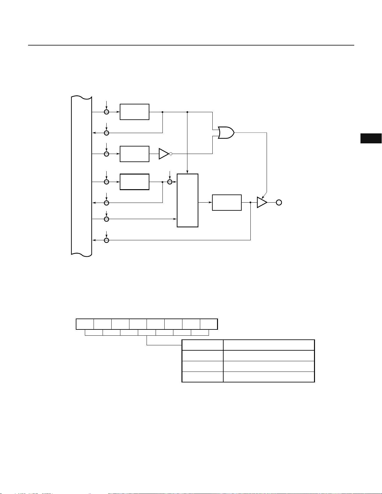
5.2.1 Hardware Configuration
Fig. 5-2 shows the hardware configuration of port 0.
Fig. 5-2 Configuration of Port 0
Chapter 5 Port Functions
WRRTPC
RDRTPC
WRPM0
WRP0L
Internal bus
RDP0L
WROUT
RDIN
Real-time output port control register
P0LM
(P0HM)
Port 0 mode register
PM0n
(PM0m)
Buffer register
P0Ln
(P0Hm)
Trigger
Selector
5.2.2 Setting the Input/Output Mode and Control Mode
Output latch
P0n
(P0m)
5
P0n
(P0m)
n = 0, 1, 2, 3
m = 4, 5, 6, 7
The port 0 mode register (PM0) sets the I/O mode of port 0, as shown in Fig. 5-3. This register is set by an 8-bit
data transfer instruction. (It can neither manipulated in bit units nor read-accessed).
Fig. 5-3 Port 0 Mode Register Format
0
PM077PM066PM055PM044PM033PM022PM011PM00
PM0
PM0
00H
FFH
Other than above
(FFH when RESET is input)
Specifies P0n pin mode (n = 0 to 7)
Output mode (output buffer ON)
High-impedance state (output buffer OFF)
Cannot be set
To use port 0 as a real-time output port, it is necessary to set the P0LM and P0HM bits of the real-time output port
control register (RTPC) to 1.
When the P0LM and P0HM bits are set, the output buffer for each pin is turned on, and the contents of the output
latch are output to the pin, regardless of the contents of the PM0.
61
Page 91

µ
PD78214 Sub-Series
5.2.3 Operation
Port 0 is an output-only port.
Once port 0 is put in the output mode, the output latch becomes operable, enabling data transfer between the
output latch and accumulator according to a transfer instruction. The output latch can be loaded with any data
by a logical operation instruction. Once the output latch is loaded with some data, it retains the data until it is
loaded with other data.
If port 0 is specified to be a real-time output port, no data can be written to the output latch. However, it is possible
to read the contents of the output latch if it is in the real-time output port mode.
Fig. 5-4 Port Specified as an Output Port
WRPORT
RDOUT
Internal bus
Output
Iatch
P0n
n = 0 to 7
5.2.4 Built-In Pull-Up Resistor
Port 0 has no built-in pull-up resistor.
5.2.5 Driving Transistors
Because port 0 has an enhanced driving capacity for the high level side of the output buffer, it can drive a transistor
directly on an active-high signal.
Fig. 5-5 shows an example of connecting a transistor to the port.
Fig. 5-5 Example of Driving a Transistor
VDD
Load
62
P0n
Page 92

Chapter 5 Port Functions
5.3 PORT 2
Port 2 is an 8-bit input-only port. P22 through P27 have a software-programmable built-in pull-up resistor. In
addition to functioning as an input port, port 2 functions as a control signal input pin such as for external interrupts
(see Table 5-3). All the 8 input pins of port 2 are configured as Schmitt trigger circuits in order to prevent
malfunction due to noise.
Table 5-3 Functions of Port 2
Port Function
P20
P21
P22
P23
P24
P25
P26
P27
Input port/NMI input
Input port/INTP0 input/CR11 capture trigger input/real-time output port trigger signal
Input port/INTP1 input/CR22 capture trigger input
Input port/INTP2 input/CI input
Input port/INTP3 input/CR02 capture trigger input
Input port/INTP4 input/ASCK input
Input port/INTP5 input/A/D controller external trigger input
Input port/SI input
Note
5
Note NMI inputs are accepted regardless of whether interrupts are enabled.
(a) Function as a port pin
Although the pins of port 0 are shared by more than one function, the level of each pin can be read and tested.
(b) Function as a control signal input pin
(i) NMI (nonmaskable interrupt)
The NMI pin receives a nonmaskable interrupt request from the outside. The external interrupt mode
register (INTM0) specifies which edge, rising or falling, is valid as an interrupt request signal.
(ii) INTP0 through INTP5 (interrupt from peripherals)
The INTP0 through INTP5 pins receive interrupt requests from the outside. An interrupt occurs when one
of these pin receives an edge specified as valid by the external interrupt mode register (INTM0 and
INTM1). (See Chapter 11.)
The INTP0 through INTP3 and INTP5 pins are also used to receive external triggers, as listed below:
• INTP0: 8-bit timer/counter 1 capture trigger input and real-time output port trigger signal
• INTP1: 8-bit timer/counter 2 capture trigger input
• INTP2: 8-bit timer/counter 2 external count clock input
• INTP3: 16-bit timer/counter 2 capture trigger input
• INTP5: A/D converter external trigger input
(iii) CI (clock input)
The CI pin receives external clock inputs for 8-bit timer/counter 2.
(iv) ASCK (asynchronous serial clock)
The ASCK pin receives a baud rate clock from the outside.
(v) SI (serial input)
The SI pin receives serial data (during three-wire serial I/O mode).
63
Page 93
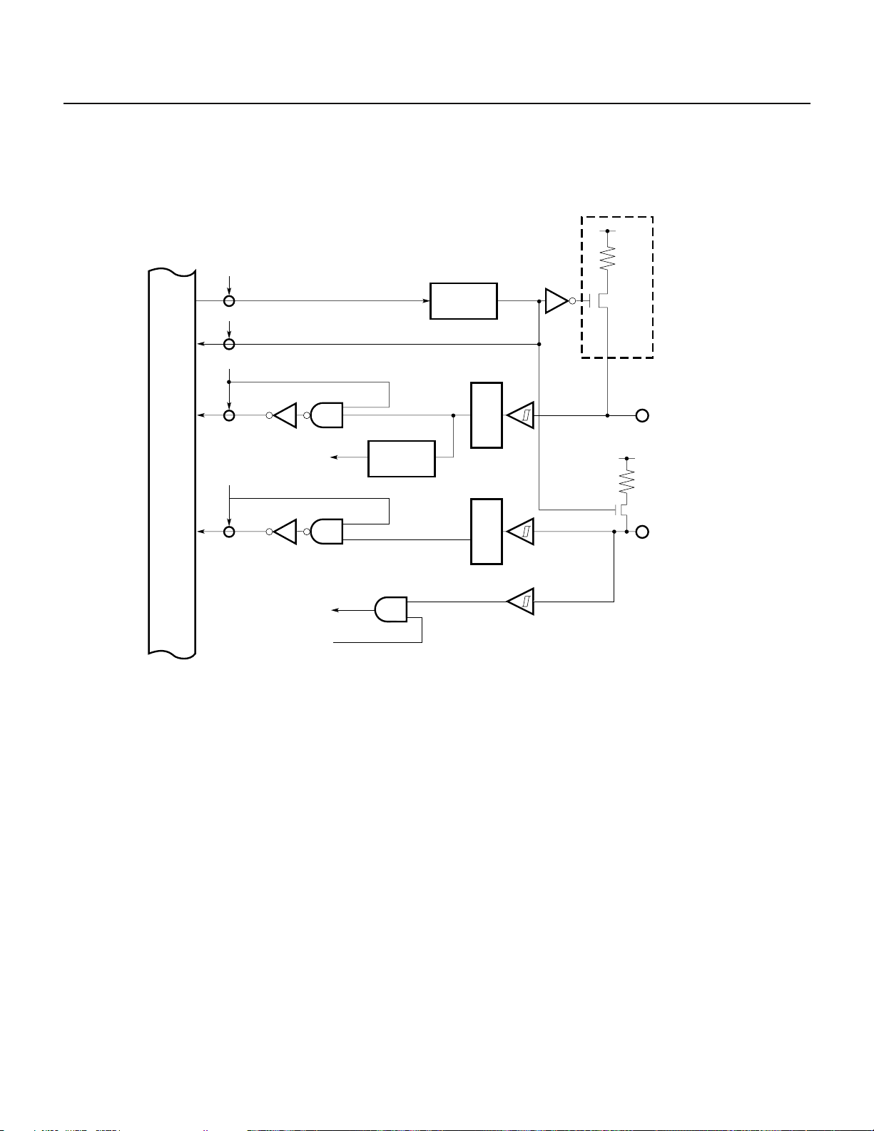
µ
PD78214 Sub-Series
5.3.1 Hardware Configuration
Fig. 5-6 shows the configuration of port 2
Fig. 5-6 Block Diagram of Port 2
V
DD
WRPUO
RDPUO
RDP2n
RDP27
Internal bus
Interrupt and
control signals
SI input
3-wire serial
I/O mode
Pull-up resistor option register
PUO2
Noise
Edge
detector
Noise
eliminator
eliminator
P2n
n = 0, 1, 2, ···, 6
P27
Note P20 or P21 does not have a circuit enclosed in a dotted box.
5.3.2 Setting the Input Mode and Control Mode
Port 2 is an input-only port.
There is no register to specify an input mode for port 2. Port 2 is always ready to receive control signals. A register
such as a control register in the hardware is used to specify what control signal to receive.
5.3.3 Operation
Port 2 is an input-only port, and the level of each pin of it can be read and tested.
For P20 through P27, the level from which noise has be removed can be read and tested. See Chapter 11 for
removing noise.
64
Page 94
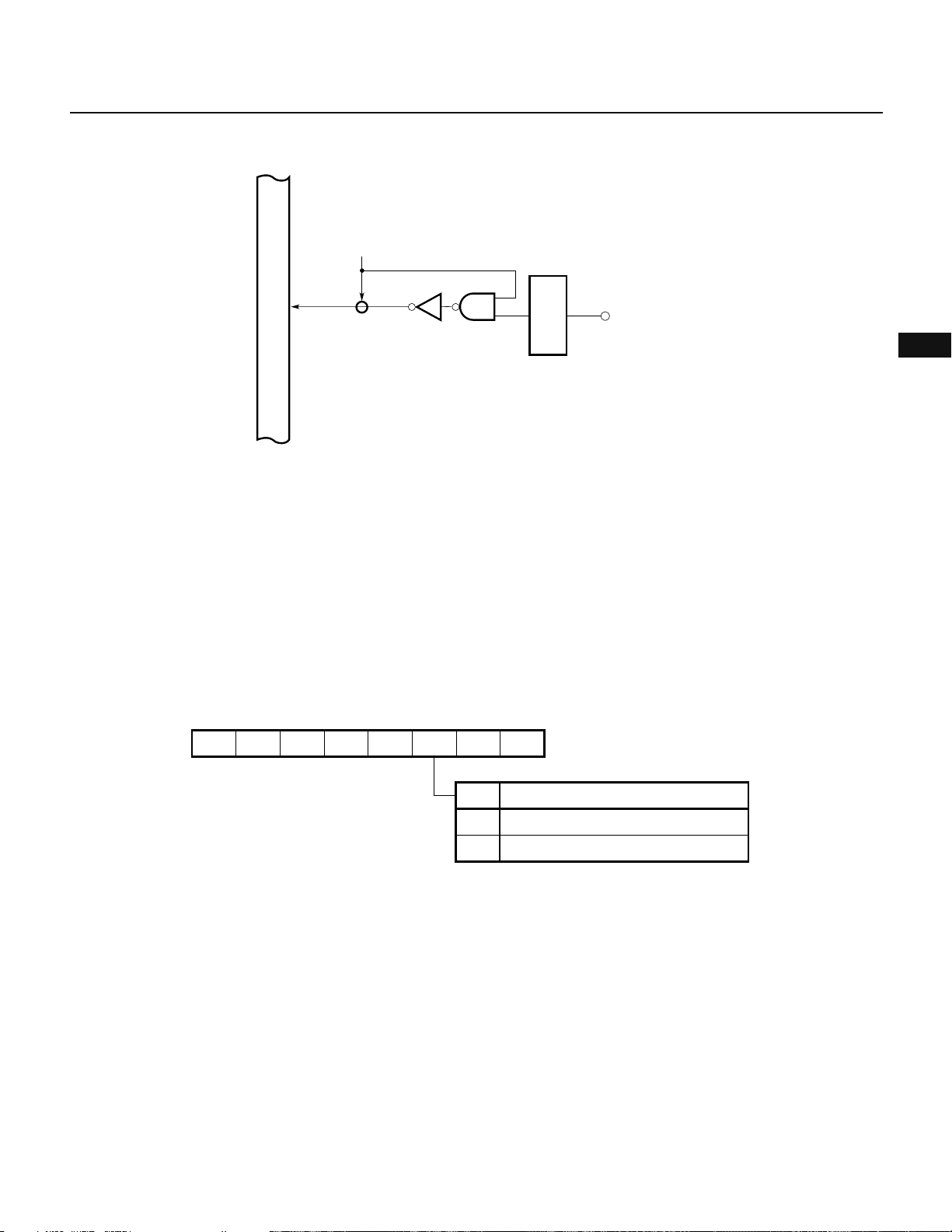
Chapter 5 Port Functions
Fig. 5-7 Port Specified as an Input Port
RDIN
P2n
Noise
Internal bus
Caution For the in-circuit emulator, the level of each port 2 pin from which noise has not been removed can be read and tested.
eliminator
5.3.4 Built-In Pull-Up Resistor
P22 through P27 have built-in pull-up resistors. When they must be pulled up, the built-in pull-up resistors should
be used. Use of the built-in pull-up resistors can reduce the number of the required components and the required
installation space.
The PUO2 bit of the pull-up-resistor-option register (PUO) can specify whether to use the built-in pull-up resistors
at P22 through P27, for all six pins at one time. (It is impossible to specify use of the built-in pull-up resistor for
an individual bit independently of the other bits.)
P20 or P21 does not have a built-in pull-up resistor.
n = 0 to 7
5
Fig. 5-8 Built-In Pull-Up Resistor Format
1
0
PUO
Remark Resetting the PUO2 bit to 00H can reduce the required current in the STOP mode.
07PUO66PUO55PUO44PUO33PUO220
PUO2
Specifies pull-up resistor connection of port 2
0
Not connected with port 2
1
Connected with pins P22 to P27
(00H when RESET is input)
0
65
Page 95
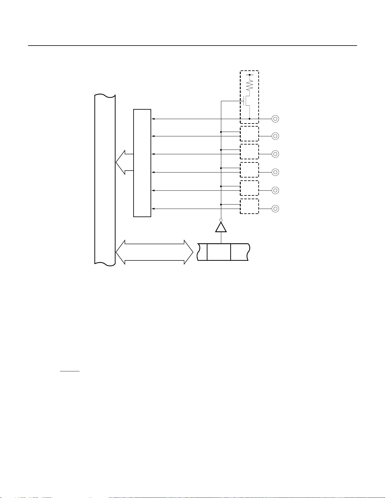
µ
PD78214 Sub-Series
Fig. 5-9 Connection of Pull-Up Resistors (Port 2)
VDD
P22
P23
P24
Input buffer
Internal bus
PUO2
Pull-up resistor option register (PUO)
Caution P22 through P26 are not pulled up immediately after a reset. In this case, INTP1 through INTP5 (one of the multiple functions
assigned to P22 to P26) may set interrupt request flags. To avoid this problem, specify use of the pull-up resistors in the initialization
routine, before clearing the interrupt flags.
P25
P26
P27
5.4 PORT 3
Port 3 is an 8-bit I/O port with an output latch. The port 3 mode register (PM3) can put each bit of this port in either
the input or output mode, separately from the other bits. Each pin has a software-programmable built-in pull-up
resistor.
In addition to I/O functions, each pin works as control signal pin.
The port 3 mode control register (PMC3) can specify the mode of operation for each pin separately from the other
pins, as listed in Table 5-4. The level of any pin can be read and tested, regardless of what function the pin is
performing.
When the RESET signal is input, port 3 becomes an input port (in the high output impedance state), and the
contents of the output latch become undefined.
66
Page 96

Table 5-4 Port 3 Operating Modes (n = 0 through 7)
Chapter 5 Port Functions
Mode Control signal I/O mode
Condition
P30
P31
P32
P33
P34
P35
P36
P37
Port mode
PMC3n = 0
I/O port
PMC3n = 1
RxD input
TxD output
SCK I/O
SO output or SB0 I/O
TO0 output
TO1 output
TO2 output
TO3 output
(a) Port mode
If a port is put in a port mode by the PMC3 register, the port mode register (PM3) can put each bit of the port
in either the input or output mode independently of the other bits.
(b) Control signal I/O mode
The PMC3 register can specify each pin of port 3 as a control pin independently of the other pins, as described
below.
(i) RxD (receive data)
The RxD pin receives serial data from the asynchronous serial interface.
(ii) TxD (transmit data)
The TxD pin outputs serial data to the asynchronous serial interface.
(iii) SCK (serial clock)
The SCK pin is a serial clock I/O pin for the clock-synchronized serial interface.
(iv) SO (serial output)/SB0 (serial bus)
The SO pin outputs serial data (during three-wire serial I/O mode). The SB0 pin is a serial bus I/O pin
(during the SBI mode).
Remark For bit 3 (P33) of port 3, “SB0” is a reserved word in the NEC assembly program package. The bit is also defined in a header
file named sfrbit.h by the C compiler.
(v) TO0 through TO3 (timer output)
The TO0 through TO3 pins are timer output pins.
5
67
Page 97

µ
PD78214 Sub-Series
5.4.1 Hardware Configuration
Fig. 5-10 through 5-13 show the configuration of port 3.
Fig. 5-10 Block Diagram of P30 (Port 3)
WRPUO
RDPUO
WRPM30
WRPMC30
RDPMC30
WRP30
Internal bus
RDP30
RDP30
RxD input
Port 3 mode register
PM30
PMC30
P30
Pull-up resistor option register
PUO3
VDD
P30
68
Page 98

Chapter 5 Port Functions
Fig. 5-11 Block Diagram of P31, and P34 through P37 (Port 3)
WRPUO
RDPUO
WRPM3n
WRPMC3n
RDPMC3n
WRP3n
Internal bus
RDP3n
RDP3n
Port 3 mode register
PM3n
PMC3n
TO, TxD output
Output latch
P3n
Pull-up resistor option register
PUO3
Selector
VDD
5
P3n
n = 1, 4, 5, 6, 7
69
Page 99

µ
PD78214 Sub-Series
★
WRPUO
RDPUO
WRPM32
WRPMC32
RDPMC32
WRP32
Internal bus
RDP32
RDP32
Fig. 5-12 Block Diagram of P32 (Port 3)
Pull-up resistor option register
PUO3
Port 3 mode register
PM32
PMC32
External
SCK
SCK
output
Output latch
P32
SCK input
VDD
P32
Selector
70
Page 100

Chapter 5 Port Functions
WRPUO
RDPUO
WRPM33
WRPMC33
RDPMC33
WRP33
Internal bus
Fig. 5-13 Block Diagram of P33 (Port 3)
Pull-up resistor option register
PUO3
Port 3 mode register
PM33
Output disable
PMC33
PMC33
SB0 output
Output latch
SO output
Selector
P33
★
5
VDD
P33
SBI mode
RDOUT
RDIN
SB0 input
PMC33
Output
disable
5.4.2 Setting the I/O Mode and Control Mode
The port 3 mode register (PM3) can put each pin of port 3 in either the input or output mode independently of the
other pins, as shown in Fig. 5-14.
The PM3 register is loaded with data using an 8-bit data transfer instruction; it cannot be bit-manipulated or readaccessed.
In addition to I/O port functions, each pin of port 3 works as a control signal pin. As shown in Fig. 5-15, the port
3 mode control register (PMC3) can specify the mode of control for each pin.
71
 Loading...