NEC PA836TF Technical data

PRELIMINARY DATA SHEET

Silicon Transistor

μPA836TF

NPN SILICON EPITAXIAL TRANSISTOR (WITH 2 DIFFERENT ELEMENTS) IN A 6-PIN THIN-TYPE SMALL MINI MOLD PACKAGE

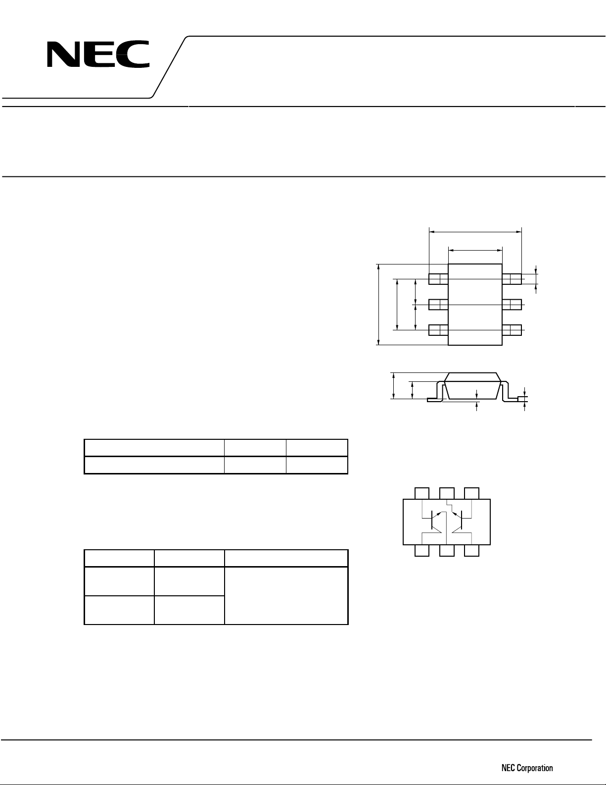
DESCRIPTION

PACKAGE DRAWINGS (Unit:mm)

The μPA836TF has two different built-in transistors (Q1 and Q2) for low noise amplification in the VHF band to UHF band.

FEATURES

Low noise

Q1 : NF = 1.5 dB TYP. @f = 2 GHz, VCE = 3 V, IC = 3 mA Q2 : NF = 1.7 dB TYP. @f = 2 GHz, VCE = 1 V, IC = 3 mA

High gain

Q1 : |S21e|2 = 8.5 dB TYP. @f = 2 GHz, VCE = 3 V, IC = 10 mA Q2 : |S21e|2 = 3.5 dB TYP. @f = 2 GHz, VCE = 1 V, IC = 3 mA

6-pin thin-type small mini mold package

2 different transistors on-chip (2SC5193, 2SC4959)

ON-CHIP TRANSISTORS


Q1

Q2


3-pin small mini mold part No.

2SC4959

2SC5193


The μPA833TF features the Q1 and Q2 in inverted positions.

ORDERING INFORMATION

PART NUMBER

QUANTITY

PACKING STYLE


μPA836TF

Loose products

8-mm wide embossed tape.


(50 pcs)

Pin 6 (Q1 Base), pin 5 (Q2


Emitter), and pin 4 (Q2 Base)

μPA836TF-T1

Taping products

face perforated side of tape.


(3 kpcs/reel)


2.10±0.1


1.25±0.1


7 4 V


+0.1 0.05

2.00±0.2

1.30

0.65 0.65

2 1

5 6

0.22


3


4


0.60±0.1

0.45

0.1

0.13±0.05


0 to


PIN CONFIGURATION (Top View)

B1 E2 B2

6 5 4


Q1


Q2


1


2


3


C1

E1

C2


PIN CONNECTIONS


1.

Collector (Q1)


4.

Base (Q2)

2.

Emitter (Q1)


5.

Emitter (Q2)

3.

Collector (Q2)


6.

Base (Q1)

Caution is required concerning excess input, such as fromcstatielectricity, because the high-frequency

process is used for this device.

The information in this document is subject to change without notice.

Document No. P12728EJ1V0DS00 (1st edition)

Date Published August 1997 N


Printed in Japan

©

1997


μPA836TF


ABSOLUTE MAXIMUM RATINGS (TA = 25°C)


PARAMETER

SYMBOL


RATING


UNIT


Q1


Q2


Collector to base voltage

VCBO

9


9


V


Collector to emitter voltage

VCEO

6


6


V


Emitter to base voltage

VEBO

2


2


V


Collector current

IC

30


100


mA


Total power dissipation

PT

150 in 1 element


150 in 1 element


mW


200 in 2 elementsNote


Junction temperature

Tj

150


150


°C


Storage temperature

Tstg


65 to +150


°C


Note 110 mW must not be exceeded for 1 element.

(1) Q1

ELECTRICAL CHARACTERISTICS

PARAMETER

SYMBOL


CONDITION

MIN.

TYP.

MAX.

UNIT


Collector cutoff current

ICBO

VCB = 5 V, IE = 0


0.1

μA


Emitter cutoff current

IEBO

VEB = 1 V, IC = 0


0.1

μA


DC current gain

hFE

VCE = 3 V, IC = 10 mANote 1

75


150


Gain bandwidth product

fT

VCE = 3

V, IC = 10 mA, f = 2 GHz


12


GHz


Feedback capacitance

Cre

VCB = 3

V, IE = 0, f = 1 MHzNote 2


0.4

0.7

pF


Insertion power gain

|S21e|2

VCE = 3

V, IC = 10 mA, f = 2 GHz

7

8.5


dB


Noise figure

NF

VCE = 3

V, IC = 3 mA, f = 2 GHz


1.5

2.5

dB


Notes 1. Pulse measurement: PW 350 μs, Duty cycle 2%

2.Collector to base capacitance when measured with capacitance meter (automatic balanced bridge method), with emitter connected to guard pin of capacitance meter.

2

μPA836TF

(2) Q2

ELECTRICAL CHARACTERISTICS

PARAMETER

SYMBOL


CONDITION

MIN.

TYP.

MAX.

UNIT


Collector cutoff current

ICBO

VCB = 5 V, IE = 0


0.1

μA


Emitter cutoff current

IEBO

VEB = 1 V, IC = 0


0.1

μA


DC current gain

hFE

VCE = 1 V, IC = 3 mANote 1

100


145


Gain bandwidth product (1)

fT

VCE = 1 V, IC = 3 mA, f = 2 GHz

4.0

4.5


GHz


Gain bandwidth product (2)

fT

VCE = 3 V, IC = 20 mA, f = 2 GHz


9.0


GHz


Feedback capacitance

Cre

VCB = 1 V, IE = 0, f = 1 MHzNote 2


0.75

0.85

pF


Insertion power gain (1)

|S21e|2

VCE = 1

V, IC = 3 mA, f = 2 GHz

2.5

3.5


dB


Insertion power gain (2)

|S21e|2

VCE = 3

V, IC = 20 mA, f = 2 GHz


6.5


dB


Noise figure (1)

NF

VCE = 1

V, IC = 3 mA, f = 2 GHz


1.7

2.5

dB


Noise figure (2)

NF

VCE = 3

V, IC = 7 mA, f = 2 GHz


1.5


dB


Notes 1. Pulse measurement: PW 350 μs, Duty cycle 2%

2.Collector to base capacitance when measured with capacitance meter (automatic balanced bridge method), with emitter connected to guard pin of capacitance meter.

hFE CLASSIFICATION

Rank

FB


Marking

V47


hFE value of Q1

75 to 150


hFE value of Q2

100 to 145


3

NEC PA836TF Technical data

TYPICAL CHARACTERISTICS (TA = 25°C)

Q1

Total Power Dissipation vs. Ambient Temperature

(mW)


Free Air


200

2 elements in total


Q1 when using 1 element


PT


dissipation


Q1 when using


2 elements


100


Total power


0

50

100

150


Ambient temperature TA (°C)


Collector Current vs. DC Base Voltage


50


VCE = 3 V


IC (mA)

40


30


current


20


Collector


10


0


0.5


1.0


DC base voltage VBE (V)


Collector Current vs. Collector to Emitter Voltage


60


500 μ A


(mA)IC

50


400

μ A


40


current


300 μ A


30


Collector


200

μ A


20


IB =

100μ A


10


0

1

2

3

4


5


6


Collector to emitter voltage VCE (V)


μPA836TF

Q2

Total Power Dissipation vs. Ambient Temperature

(mW)


2 elements in total

Free Air


200


Q2 when using 1 element


PT


dissipation


Q2 when using


2 elements


100


Total power


0

50

100


150


Ambient temperature TA (°C)


Collector Current vs. DC Base Voltage


100


50


VCE = 1 V


(mA)

20


10


IC

5


current

2


1


Collector

0.5


0.2


0.1


0.05


0.02


0.01


0.5


1


0


DC base voltage VBE (V)


Collector Current vs. Collector to Emitter Voltage


30


200

μ A


(mA)IC

20


180

μ A


160

μ A


current


140

μ A


100

μ A


120

μ A


Collector

10


80

μ A


60

μ A


40

μ A


IB = 20 μ A


0

1

2

3

4

5

6


Collector to emitter voltage VCE (V)

4

Loading...
+ 8 hidden pages