

User’s Manual
78K0/KE2
8-Bit Single-Chip Microcontrollers
µ
PD78F0531
µ
PD78F0531(A)
µ
PD78F0531(A2)
µ
PD78F0532
µ
PD78F0533
µ
PD78F0534
µ
PD78F0535
µ
PD78F0536
µ
PD78F0537
µ
PD78F0537D
The µPD78F0537D has an on-chip debug function.
Do not use this product for mass production because its reliability cannot be guaranteed after the on-chip debug function
has been used, due to issues with respect to the number of times the flash memory can be rewritten. NEC Electronics
does not accept complaints concerning this product.
Document No. U17260EJ6V0UD00 (6th edition)
Date Published September 2007 NS
µ
PD78F0532(A)
µ
PD78F0533(A)
µ
PD78F0534(A)
µ
PD78F0535(A)
µ
PD78F0536(A)
µ
PD78F0537(A)
µ
PD78F0532(A2)
µ
PD78F0533(A2)
µ
PD78F0534(A2)
µ
PD78F0535(A2)
µ
PD78F0536(A2)
µ
PD78F0537(A2)
Printed in Japan
2004

[MEMO]
2
User’s Manual U17260EJ6V0UD

NOTES FOR CMOS DEVICES
1
VOLTAGE APPLICATION WAVEFORM AT INPUT PIN
Waveform distortion due to input noise or a reflected wave may cause malfunction. If the input of the
CMOS device stays in the area between V
malfunction. Take care to prevent chattering noise from entering the device when the input level is fixed,
and also in the transition period when the input level passes through the area between V
V
IH
(MIN).
HANDLING OF UNUSED INPUT PINS
2
Unconnected CMOS device inputs can be cause of malfunction. If an input pin is unconnected, it is
possible that an internal input level may be generated due to noise, etc., causing malfunction. CMOS
devices behave differently than Bipolar or NMOS devices. Input levels of CMOS devices must be fixed
high or low by using pull-up or pull-down circuitry. Each unused pin should be connected to V
via a resistor if there is a possibility that it will be an output pin. All handling related to unused pins must
be judged separately for each device and according to related specifications governing the device.
3
PRECAUTION AGAINST ESD
A strong electric field, when exposed to a MOS device, can cause destruction of the gate oxide and
ultimately degrade the device operation. Steps must be taken to stop generation of static electricity as
much as possible, and quickly dissipate it when it has occurred. Environmental control must be
adequate. When it is dry, a humidifier should be used. It is recommended to avoid using insulators that
easily build up static electricity. Semiconductor devices must be stored and transported in an anti-static
container, static shielding bag or conductive material. All test and measurement tools including work
benches and floors should be grounded. The operator should be grounded using a wrist strap.
Semiconductor devices must not be touched with bare hands. Similar precautions need to be taken for
PW boards with mounted semiconductor devices.
IL
(MAX) and VIH (MIN) due to noise, etc., the device may
IL
(MAX) and
DD
or GND
4
STATUS BEFORE INITIALIZATION
Power-on does not necessarily define the initial status of a MOS device. Immediately after the power
source is turned ON, devices with reset functions have not yet been initialized. Hence, power-on does
not guarantee output pin levels, I/O settings or contents of registers. A device is not initialized until the
reset signal is received. A reset operation must be executed immediately after power-on for devices
with reset functions.
5
POWER ON/OFF SEQUENCE
In the case of a device that uses different power supplies for the internal operation and external
interface, as a rule, switch on the external power supply after switching on the internal power supply.
When switching the power supply off, as a rule, switch off the external power supply and then the
internal power supply. Use of the reverse power on/off sequences may result in the application of an
overvoltage to the internal elements of the device, causing malfunction and degradation of internal
elements due to the passage of an abnormal current.
The correct power on/off sequence must be judged separately for each device and according to related
specifications governing the device.
6
INPUT OF SIGNAL DURING POWER OFF STATE
Do not input signals or an I/O pull-up power supply while the device is not powered. The current
injection that results from input of such a signal or I/O pull-up power supply may cause malfunction and
the abnormal current that passes in the device at this time may cause degradation of internal elements.
Input of signals during the power off state must be judged separately for each device and according to
related specifications governing the device.
User’s Manual U17260EJ6V0UD
3

EEPROM is a trademark of NEC Electronics Corporation.
Windows and Windows NT are registered trademarks or trademarks of Microsoft Corporation in the United
States and/or other countries.
PC/AT is a trademark of International Business Machines Corporation.
HP9000 series 700 and HP-UX are trademarks of Hewlett-Packard Company.
SPARCstation is a trademark of SPARC International, Inc.
Solaris and SunOS are trademarks of Sun Microsystems, Inc.
SuperFlash
is a registered trademark of Silicon Storage Technology, Inc. in several countries including the
United States and Japan.
4
User’s Manual U17260EJ6V0UD

Caution: This product uses SuperFlash
®
technology licensed from Silicon Storage Technology, Inc.
•
The information in this document is current as of September, 2007. The information is subject to
change without notice. For actual design-in, refer to the latest publications of NEC Electronics data
sheets or data books, etc., for the most up-to-date specifications of NEC Electronics products. Not
all products and/or types are available in every country. Please check with an NEC Electronics sales
representative for availability and additional information.
No part of this document may be copied or reproduced in any form or by any means without the prior
•
written consent of NEC Electronics. NEC Electronics assumes no responsibility for any errors that may
appear in this document.
•
NEC Electronics does not assume any liability for infringement of patents, copyrights or other intellectual
property rights of third parties by or arising from the use of NEC Electronics products listed in this document
or any other liability arising from the use of such products. No license, express, implied or otherwise, is
granted under any patents, copyrights or other intellectual property rights of NEC Electronics or others.
Descriptions of circuits, software and other related information in this document are provided for illustrative
•
purposes in semiconductor product operation and application examples. The incorporation of these
circuits, software and information in the design of a customer's equipment shall be done under the full
responsibility of the customer. NEC Electronics assumes no responsibility for any losses incurred by
customers or third parties arising from the use of these circuits, software and information.
•
While NEC Electronics endeavors to enhance the quality, reliability and safety of NEC Electronics products,
customers agree and acknowledge that the possibility of defects thereof cannot be eliminated entirely. To
minimize risks of damage to property or injury (including death) to persons arising from defects in NEC
Electronics products, customers must incorporate sufficient safety measures in their design, such as
redundancy, fire-containment and anti-failure features.
•
NEC Electronics products are classified into the following three quality grades: "Standard", "Special" and
"Specific".
The "Specific" quality grade applies only to NEC Electronics products developed based on a customerdesignated "quality assurance program" for a specific application. The recommended applications of an NEC
Electronics product depend on its quality grade, as indicated below. Customers must check the quality grade of
each NEC Electronics product before using it in a particular application.
"Standard":
"Special":
"Specific":
Computers, office equipment, communications equipment, test and measurement equipment, audio
and visual equipment, home electronic appliances, machine tools, personal electronic equipment
and industrial robots.
Transportation equipment (automobiles, trains, ships, etc.), traffic control systems, anti-disaster
systems, anti-crime systems, safety equipment and medical equipment (not specifically designed
for life support).
Aircraft, aerospace equipment, submersible repeaters, nuclear reactor control systems, life
support systems and medical equipment for life support, etc.
The quality grade of NEC Electronics products is "Standard" unless otherwise expressly specified in NEC
Electronics data sheets or data books, etc. If customers wish to use NEC Electronics products in applications
not intended by NEC Electronics, they must contact an NEC Electronics sales representative in advance to
determine NEC Electronics' willingness to support a given application.
(Note)
(1)
"NEC Electronics" as used in this statement means NEC Electronics Corporation and also includes its
majority-owned subsidiaries.
(2)
"NEC Electronics products" means any product developed or manufactured by or for NEC Electronics (as
defined above).
M8 E 02 . 11-1
User’s Manual U17260EJ6V0UD
5

INTRODUCTION
Readers This manual is intended for user engineers who wish to understand the functions of the
78K0/KE2 and design and develop application systems and programs for these devices.
The target products are as follows.
78K0/KE2:
78F0537D, 78F0531(A), 78F0532(A), 78F0533(A), 78F0534(A),
<R>
Purpose This manual is intended to give users an understanding of the functions described in the
Organization below.
Organization The 78K0/KE2 manual is separated into two parts: this manual and the instructions
edition (common to the 78K0 microcontrollers).
µ
PD78F0531, 78F0532, 78F0533, 78F0534, 78F0535, 78F0536, 78F0537,
78F0535(A), 78F0536(A), 78F0537(A), 78F0531(A2), 78F0532(A2),
78F0533(A2), 78F0534(A2), 78F0535(A2), 78F0536(A2), 78F0537(A2)
78K0/KE2
User’s Manual
(This Manual)
• Pin functions
• Internal block functions
• Interrupts
• Other on-chip peripheral functions
• Electrical specifications
How to Read This Manual It is assumed that the readers of this manual have general knowledge of electrical
engineering, logic circuits, and microcontrollers.
<R>
• When using this manual as the manual for (A) grade products and (A2) grade
products:
→ Only the quality grade differs between standard products, (A) grade products, and
(A2) grade products. Read the part number as follows.
•
µ
PD78F0531→ µPD78F0531(A), µPD78F0531(A2)
•
µ
PD78F0532→ µPD78F0532(A), µPD78F0532(A2)
•
µ
PD78F0533→ µPD78F0533(A), µPD78F0533(A2)
•
µ
PD78F0534→ µPD78F0534(A), µPD78F0534(A2)
•
µ
PD78F0535→ µPD78F0535(A), µPD78F0535(A2)
•
µ
PD78F0536→ µPD78F0536(A), µPD78F0536(A2)
•
µ
PD78F0537→ µPD78F0537(A), µPD78F0537(A2)
• To gain a general understanding of functions:
→ Read this manual in the order of the CONTENTS. The mark “<R>” shows major
revised points. The revised points can be easily searched by copying an “<R>” in
the PDF file and specifying it in the “Find what:” field.
78K/0 Series
User’s Manual
Instructions
• CPU functions
• Instruction set
• Explanation of each instruction
6
User’s Manual U17260EJ6V0UD

• How to interpret the register format:
→ For a bit number enclosed in angle brackets, the bit name is defined as a
reserved word in the RA78K0, and is defined as an sfr variable using the
#pragma sfr directive in the CC78K0.
• To check the details of a register when you know the register name:
→ See APPENDIX C REGISTER INDEX.
• To know details of the 78K0 microcontroller instructions:
→ Refer to the separate document 78K/0 Series Instructions User’s Manual
(U12326E).
Conventions Data significance: Higher digits on the left and lower digits on the right
Active low representations: ××× (overscore over pin and signal name)
Note: Footnote for item marked with Note in the text
Caution: Information requiring particular attention
Remark: Supplementary information
Numerical representations: Binary
Decimal
Hexadecimal
...
×××× or ××××B
...
××××
...
××××H
Related Documents The related documents indicated in this publication may include preliminary versions.
However, preliminary versions are not marked as such.
Documents Related to Devices
<R>
Document Name Document No.
78K0/KE2 User’s Manual This manual
78K/0 Series Instructions User’s Manual U12326E
78K0/Kx2 Flash Memory Programming (Programmer) Application Note U17739E
78K0/Kx2 Flash Memory Self Programming User’s Manual
78K0/Kx2 EEPROMTM Emulation Application Note
Note
Note
U17516E
U17517E
Note This document is under engineering management. For details, consult an NEC
Electronics sales representative.
Documents Related to Development Tools (Software) (User’s Manuals)
Document Name Document No.
RA78K0 Ver. 3.80 Assembler Package
ID78K0-QB Ver. 2.90 Integrated Debugger Operation U17437E
PM+ Ver. 5.20 U16934E
Operation U17199E
Language U17198E
Structured Assembly Language U17197E
Operation U17201E CC78K0 Ver. 3.70 C Compiler
Language U17200E
Operation U17246E SM+ System Simulator
User Open Interface U17247E
Caution The related documents listed above are subject to change without notice. Be sure to use the latest
version of each document when designing.
User’s Manual U17260EJ6V0UD
7

Documents Related to Development Tools (Hardware) (User’s Manuals)
Document Name Document No.
QB-78K0KX2 In-Circuit Emulator U17341E
QB-78K0MINI On-Chip Debug Emulator U17029E
<R>
QB-MINI2 On-Chip Debug Emulator with Programming Function U18371E
Documents Related to Flash Memory Programming
Document Name Document No.
PG-FP4 Flash Memory Programmer User’s Manual U15260E
PG-FPL3 Flash Memory Programmer User’s Manual U17454E
Other Documents
Document Name Document No.
SEMICONDUCTOR SELECTION GUIDE − Products and Packages − X13769X
Semiconductor Device Mount Manual Note
Quality Grades on NEC Semiconductor Devices C11531E
NEC Semiconductor Device Reliability/Quality Control System C10983E
Guide to Prevent Damage for Semiconductor Devices by Electrostatic Discharge (ESD) C11892E
Note See the “Semiconductor Device Mount Manual” website (http://www.necel.com/pkg/en/mount/index.html).
Caution The related documents listed above are subject to change without notice. Be sure to use the latest
version of each document when designing.
8
User’s Manual U17260EJ6V0UD

CONTENTS
CHAPTER 1 OUTLINE ............................................................................................................................ 17
1.1 Features ........................................................................................................................................ 17
1.2 Applications.................................................................................................................................. 18
1.3 Ordering Information ................................................................................................................... 19
1.4 Pin Configuration (Top View)...................................................................................................... 22
1.5 78K0/Kx2 Microcontroller Lineup............................................................................................... 25
1.6 Block Diagram .............................................................................................................................. 28
1.7 Outline of Functions .................................................................................................................... 29
CHAPTER 2 PIN FUNCTIONS ............................................................................................................... 32
2.1 Pin Function List .......................................................................................................................... 32
2.2 Description of Pin Functions ...................................................................................................... 36
2.2.1 P00 to P06 (port 0)...........................................................................................................................36
2.2.2 P10 to P17 (port 1)...........................................................................................................................37
2.2.3 P20 to P27 (port 2)...........................................................................................................................38
2.2.4 P30 to P33 (port 3)...........................................................................................................................38
2.2.5 P40 to P43 (port 4)...........................................................................................................................39
2.2.6 P50 to P53 (port 5)...........................................................................................................................39
2.2.7 P60 to P63 (port 6)...........................................................................................................................39
2.2.8 P70 to P77 (port 7)...........................................................................................................................39
2.2.9 P120 to P124 (port 12).....................................................................................................................40
2.2.10 P130 (port 13)................................................................................................................................41
2.2.11 P140, P141 (port 14)......................................................................................................................41
2.2.12 AVREF .............................................................................................................................................41
2.2.13 AVSS............................................................................................................................................... 42
2.2.14 RESET...........................................................................................................................................42
2.2.15 REGC ............................................................................................................................................42
2.2.16 VDD and EVDD.................................................................................................................................42
2.2.17 VSS and EVSS .................................................................................................................................42
2.2.18 FLMD0 ........................................................................................................................................... 42
2.3 Pin I/O Circuits and Recommended Connection of Unused Pins........................................... 43
CHAPTER 3 CPU ARCHITECTURE ...................................................................................................... 47
3.1 Memory Space.............................................................................................................................. 47
3.1.1 Internal program memory space ......................................................................................................58
3.1.2 Memory bank (µPD78F0536, 78F0537, and 78F0537D only) .........................................................60
3.1.3 Internal data memory space ............................................................................................................60
3.1.4 Special function register (SFR) area................................................................................................61
3.1.5 Data memory addressing.................................................................................................................61
3.2 Processor Registers .................................................................................................................... 69
3.2.1 Control registers...............................................................................................................................69
3.2.2 General-purpose registers ...............................................................................................................73
3.2.3 Special function registers (SFRs).....................................................................................................74
3.3 Instruction Address Addressing ................................................................................................ 79
3.3.1 Relative addressing .........................................................................................................................79
User’s Manual U17260EJ6V0UD
9

3.3.2 Immediate addressing..................................................................................................................... 80
3.3.3 Table indirect addressing ................................................................................................................ 81
3.3.4 Register addressing ........................................................................................................................ 82
3.4 Operand Address Addressing .................................................................................................... 82
3.4.1 Implied addressing .......................................................................................................................... 82
3.4.2 Register addressing ........................................................................................................................ 83
3.4.3 Direct addressing ............................................................................................................................ 84
3.4.4 Short direct addressing ................................................................................................................... 85
3.4.5 Special function register (SFR) addressing..................................................................................... 86
3.4.6 Register indirect addressing............................................................................................................ 87
3.4.7 Based addressing ........................................................................................................................... 88
3.4.8 Based indexed addressing.............................................................................................................. 89
3.4.9 Stack addressing............................................................................................................................. 90
CHAPTER 4 MEMORY BANK SELECT FUNCTION (µPD78F0536, 78F0537, AND 78F0537D
ONLY) ............................................................................................................................... 91
4.1 Memory Bank ................................................................................................................................ 91
4.2 Difference in Representation of Memory Space ....................................................................... 92
4.3 Memory Bank Select Register (BANK) ....................................................................................... 93
4.4 Selecting Memory Bank............................................................................................................... 94
4.4.1 Referencing values between memory banks................................................................................... 94
4.4.2 Branching instruction between memory banks................................................................................ 96
4.4.3 Subroutine call between memory banks ......................................................................................... 98
4.4.4 Instruction branch to bank area by interrupt...................................................................................100
CHAPTER 5 PORT FUNCTIONS ......................................................................................................... 102
5.1 Port Functions ............................................................................................................................ 102
5.2 Port Configuration...................................................................................................................... 104
5.2.1 Port 0 .............................................................................................................................................105
5.2.2 Port 1 .............................................................................................................................................111
5.2.3 Port 2 .............................................................................................................................................116
5.2.4 Port 3 .............................................................................................................................................117
5.2.5 Port 4 .............................................................................................................................................120
5.2.6 Port 5 .............................................................................................................................................121
5.2.7 Port 6 .............................................................................................................................................122
5.2.8 Port 7 .............................................................................................................................................124
5.2.9 Port 12 ...........................................................................................................................................125
5.2.10 Port 13 .........................................................................................................................................128
5.2.11 Port 14 .........................................................................................................................................129
5.3 Registers Controlling Port Function ........................................................................................ 130
5.4 Port Function Operations .......................................................................................................... 135
5.4.1 Writing to I/O port...........................................................................................................................135
5.4.2 Reading from I/O port.....................................................................................................................135
5.4.3 Operations on I/O port....................................................................................................................135
5.5 Settings of Port Mode Register and Output Latch When Using Alternate Function........... 136
5.6 Cautions on 1-Bit Manipulation Instruction for Port Register n (Pn).................................... 139
CHAPTER 6 CLOCK GENERATOR .................................................................................................... 140
6.1 Functions of Clock Generator................................................................................................... 140
10
User’s Manual U17260EJ6V0UD

6.2 Configuration of Clock Generator ............................................................................................ 141
6.3 Registers Controlling Clock Generator ................................................................................... 143
6.4 System Clock Oscillator ............................................................................................................ 152
6.4.1 X1 oscillator ...................................................................................................................................152
6.4.2 XT1 oscillator .................................................................................................................................152
6.4.3 When subsystem clock is not used................................................................................................155
6.4.4 Internal high-speed oscillator .........................................................................................................155
6.4.5 Internal low-speed oscillator ..........................................................................................................155
6.4.6 Prescaler........................................................................................................................................155
6.5 Clock Generator Operation ....................................................................................................... 156
6.6 Controlling Clock ....................................................................................................................... 160
6.6.1 Controlling high-speed system clock..............................................................................................160
6.6.2 Example of controlling internal high-speed oscillation clock ..........................................................163
6.6.3 Example of controlling subsystem clock ........................................................................................165
6.6.4 Example of controlling internal low-speed oscillation clock............................................................167
6.6.5 Clocks supplied to CPU and peripheral hardware .........................................................................167
6.6.6 CPU clock status transition diagram ..............................................................................................168
6.6.7 Condition before changing CPU clock and processing after changing CPU clock ......................... 173
6.6.8 Time required for switchover of CPU clock and main system clock ...............................................174
6.6.9 Conditions before clock oscillation is stopped................................................................................ 175
6.6.10 Peripheral hardware and source clocks .......................................................................................176
CHAPTER 7 16-BIT TIMER/EVENT COUNTERS 00 AND 01 ........................................................ 177
7.1 Functions of 16-Bit Timer/Event Counters 00 and 01............................................................. 177
7.2 Configuration of 16-Bit Timer/Event Counters 00 and 01 ...................................................... 178
7.3 Registers Controlling 16-Bit Timer/Event Counters 00 and 01 ............................................. 184
7.4 Operation of 16-Bit Timer/Event Counters 00 and 01............................................................. 196
7.4.1 Interval timer operation ..................................................................................................................196
7.4.2 Square-wave output operation.......................................................................................................199
7.4.3 External event counter operation ...................................................................................................202
7.4.4 Operation in clear & start mode entered by TI00n pin valid edge input..........................................206
7.4.5 Free-running timer operation .........................................................................................................220
7.4.6 PPG output operation ....................................................................................................................229
7.4.7 One-shot pulse output operation.................................................................................................... 232
7.4.8 Pulse width measurement operation..............................................................................................237
7.5 Special Use of TM0n .................................................................................................................. 245
7.5.1 Rewriting CR01n during TM0n operation.......................................................................................245
7.5.2 Setting LVS0n and LVR0n ............................................................................................................. 245
7.6 Cautions for 16-Bit Timer/Event Counters 00 and 01............................................................. 247
CHAPTER 8 8-BIT TIMER/EVENT COUNTERS 50 AND 51 .......................................................... 251
8.1 Functions of 8-Bit Timer/Event Counters 50 and 51............................................................... 251
8.2 Configuration of 8-Bit Timer/Event Counters 50 and 51 ........................................................ 251
8.3 Registers Controlling 8-Bit Timer/Event Counters 50 and 51 ............................................... 254
8.4 Operations of 8-Bit Timer/Event Counters 50 and 51............................................................. 259
8.4.1 Operation as interval timer.............................................................................................................259
8.4.2 Operation as external event counter .............................................................................................. 261
8.4.3 Square-wave output operation.......................................................................................................262
8.4.4 PWM output operation ...................................................................................................................263
User’s Manual U17260EJ6V0UD
11

8.5 Cautions for 8-Bit Timer/Event Counters 50 and 51 ............................................................... 267
CHAPTER 9 8-BIT TIMERS H0 AND H1 .......................................................................................... 268
9.1 Functions of 8-Bit Timers H0 and H1 ....................................................................................... 268
9.2 Configuration of 8-Bit Timers H0 and H1................................................................................. 268
9.3 Registers Controlling 8-Bit Timers H0 and H1 ........................................................................ 272
9.4 Operation of 8-Bit Timers H0 and H1........................................................................................ 278
9.4.1 Operation as interval timer/square-wave output.............................................................................278
9.4.2 Operation as PWM output..............................................................................................................281
9.4.3 Carrier generator operation (8-bit timer H1 only)............................................................................287
CHAPTER 10 WATCH TIMER.............................................................................................................. 294
10.1 Functions of Watch Timer ....................................................................................................... 294
10.2 Configuration of Watch Timer................................................................................................. 295
10.3 Register Controlling Watch Timer .......................................................................................... 296
10.4 Watch Timer Operations.......................................................................................................... 298
10.4.1 Watch timer operation ..................................................................................................................298
10.4.2 Interval timer operation ................................................................................................................298
10.5 Cautions for Watch Timer........................................................................................................ 299
CHAPTER 11 WATCHDOG TIMER ..................................................................................................... 300
11.1 Functions of Watchdog Timer................................................................................................. 300
11.2 Configuration of Watchdog Timer .......................................................................................... 301
11.3 Register Controlling Watchdog Timer.................................................................................... 302
11.4 Operation of Watchdog Timer................................................................................................. 303
11.4.1 Controlling operation of watchdog timer.......................................................................................303
11.4.2 Setting overflow time of watchdog timer.......................................................................................304
11.4.3 Setting window open period of watchdog timer............................................................................305
CHAPTER 12 CLOCK OUTPUT/BUZZER OUTPUT CONTROLLER............................................... 307
12.1 Functions of Clock Output/Buzzer Output Controller .......................................................... 307
12.2 Configuration of Clock Output/Buzzer Output Controller.................................................... 308
12.3 Registers Controlling Clock Output/Buzzer Output Controller ........................................... 308
12.4 Operations of Clock Output/Buzzer Output Controller ........................................................ 311
12.4.1 Operation as clock output ............................................................................................................311
12.4.2 Operation as buzzer output..........................................................................................................311
CHAPTER 13 A/D CONVERTER ......................................................................................................... 312
13.1 Function of A/D Converter....................................................................................................... 312
13.2 Configuration of A/D Converter .............................................................................................. 313
13.3 Registers Used in A/D Converter............................................................................................ 315
13.4 A/D Converter Operations ....................................................................................................... 323
13.4.1 Basic operations of A/D converter................................................................................................323
13.4.2 Input voltage and conversion results............................................................................................325
13.4.3 A/D converter operation mode .....................................................................................................326
13.5 How to Read A/D Converter Characteristics Table............................................................... 328
13.6 Cautions for A/D Converter ..................................................................................................... 330
12
User’s Manual U17260EJ6V0UD

CHAPTER 14 SERIAL INTERFACE UART0 ...................................................................................... 334
14.1 Functions of Serial Interface UART0...................................................................................... 334
14.2 Configuration of Serial Interface UART0 ............................................................................... 335
14.3 Registers Controlling Serial Interface UART0....................................................................... 338
14.4 Operation of Serial Interface UART0...................................................................................... 343
14.4.1 Operation stop mode ...................................................................................................................343
14.4.2 Asynchronous serial interface (UART) mode...............................................................................344
14.4.3 Dedicated baud rate generator ....................................................................................................350
14.4.4 Calculation of baud rate ...............................................................................................................351
CHAPTER 15 SERIAL INTERFACE UART6 ...................................................................................... 355
15.1 Functions of Serial Interface UART6...................................................................................... 355
15.2 Configuration of Serial Interface UART6 ............................................................................... 359
15.3 Registers Controlling Serial Interface UART6....................................................................... 362
15.4 Operation of Serial Interface UART6...................................................................................... 371
15.4.1 Operation stop mode ...................................................................................................................371
15.4.2 Asynchronous serial interface (UART) mode...............................................................................372
15.4.3 Dedicated baud rate generator ....................................................................................................385
15.4.4 Calculation of baud rate ...............................................................................................................387
CHAPTER 16 SERIAL INTERFACES CSI10 AND CSI11................................................................ 392
16.1 Functions of Serial Interfaces CSI10 and CSI11 ................................................................... 392
16.2 Configuration of Serial Interfaces CSI10 and CSI11............................................................. 393
16.3 Registers Controlling Serial Interfaces CSI10 and CSI11 .................................................... 396
16.4 Operation of Serial Interfaces CSI10 and CSI11 ................................................................... 402
16.4.1 Operation stop mode ...................................................................................................................402
16.4.2 3-wire serial I/O mode..................................................................................................................403
CHAPTER 17 SERIAL INTERFACE IIC0 ........................................................................................... 415
17.1 Functions of Serial Interface IIC0 ........................................................................................... 415
17.2 Configuration of Serial Interface IIC0..................................................................................... 418
17.3 Registers to Control Serial Interface IIC0.............................................................................. 421
17.4 I2C Bus Mode Functions .......................................................................................................... 434
17.4.1 Pin configuration ..........................................................................................................................434
17.5 I2C Bus Definitions and Control Methods .............................................................................. 435
17.5.1 Start conditions ............................................................................................................................435
17.5.2 Addresses....................................................................................................................................436
17.5.3 Transfer direction specification ....................................................................................................436
17.5.4 Acknowledge (ACK).....................................................................................................................437
17.5.5 Stop condition ..............................................................................................................................438
17.5.6 Wait..............................................................................................................................................439
17.5.7 Canceling wait..............................................................................................................................441
17.5.8 Interrupt request (INTIIC0) generation timing and wait control ....................................................441
17.5.9 Address match detection method ................................................................................................442
17.5.10 Error detection ...........................................................................................................................442
17.5.11 Extension code ..........................................................................................................................443
17.5.12 Arbitration ..................................................................................................................................444
17.5.13 Wakeup function ........................................................................................................................445
User’s Manual U17260EJ6V0UD
13

17.5.14 Communication reservation........................................................................................................446
17.5.15 Other cautions............................................................................................................................449
17.5.16 Communication operations.........................................................................................................451
17.5.17 Timing of I2C interrupt request (INTIIC0) occurrence .................................................................459
17.6 Timing Charts ........................................................................................................................... 480
CHAPTER 18 MULTIPLIER/DIVIDER (µPD78F0534, 78F0535, 78F0536, 78F0537, AND
78F0537D ONLY) .......................................................................................................... 487
18.1 Functions of Multiplier/Divider................................................................................................ 487
18.2 Configuration of Multiplier/Divider ......................................................................................... 487
18.3 Register Controlling Multiplier/Divider................................................................................... 491
18.4 Operations of Multiplier/Divider.............................................................................................. 492
18.4.1 Multiplication operation ................................................................................................................492
18.4.2 Division operation.........................................................................................................................494
CHAPTER 19 INTERRUPT FUNCTIONS ............................................................................................ 496
19.1 Interrupt Function Types ......................................................................................................... 496
19.2 Interrupt Sources and Configuration ..................................................................................... 496
19.3 Registers Controlling Interrupt Functions............................................................................. 501
19.4 Interrupt Servicing Operations ............................................................................................... 508
19.4.1 Maskable interrupt acknowledgement..........................................................................................508
19.4.2 Software interrupt request acknowledgement ..............................................................................510
19.4.3 Multiple interrupt servicing ...........................................................................................................511
19.4.4 Interrupt request hold ...................................................................................................................514
CHAPTER 20 KEY INTERRUPT FUNCTION ..................................................................................... 515
20.1 Functions of Key Interrupt ...................................................................................................... 515
20.2 Configuration of Key Interrupt ................................................................................................ 515
20.3 Register Controlling Key Interrupt ......................................................................................... 516
CHAPTER 21 STANDBY FUNCTION .................................................................................................. 517
21.1 Standby Function and Configuration..................................................................................... 517
21.1.1 Standby function ..........................................................................................................................517
21.1.2 Registers controlling standby function..........................................................................................517
21.2 Standby Function Operation ................................................................................................... 520
21.2.1 HALT mode..................................................................................................................................520
21.2.2 STOP mode .................................................................................................................................525
CHAPTER 22 RESET FUNCTION........................................................................................................ 531
22.1 Register for Confirming Reset Source................................................................................... 539
CHAPTER 23 POWER-ON-CLEAR CIRCUIT...................................................................................... 540
23.1 Functions of Power-on-Clear Circuit...................................................................................... 540
23.2 Configuration of Power-on-Clear Circuit ............................................................................... 541
23.3 Operation of Power-on-Clear Circuit...................................................................................... 541
23.4 Cautions for Power-on-Clear Circuit ...................................................................................... 544
CHAPTER 24 LOW-VOLTAGE DETECTOR ....................................................................................... 546
24.1 Functions of Low-Voltage Detector........................................................................................ 546
14
User’s Manual U17260EJ6V0UD

24.2 Configuration of Low-Voltage Detector ................................................................................. 547
24.3 Registers Controlling Low-Voltage Detector ........................................................................ 547
24.4 Operation of Low-Voltage Detector........................................................................................ 550
24.4.1 When used as reset ..................................................................................................................... 551
24.4.2 When used as interrupt................................................................................................................556
24.5 Cautions for Low-Voltage Detector........................................................................................ 561
CHAPTER 25 OPTION BYTE............................................................................................................... 564
25.1 Functions of Option Bytes ...................................................................................................... 564
25.2 Format of Option Byte ............................................................................................................. 566
CHAPTER 26 FLASH MEMORY.......................................................................................................... 569
26.1 Internal Memory Size Switching Register.............................................................................. 569
26.2 Internal Expansion RAM Size Switching Register................................................................ 571
26.3 Writing with Flash Memory Programmer............................................................................... 572
26.4 Programming Environment..................................................................................................... 575
26.5 Communication Mode.............................................................................................................. 575
26.6 Handling of Pins on Board ...................................................................................................... 577
26.6.1 FLMD0 pin ...................................................................................................................................577
26.6.2 Serial interface pins .....................................................................................................................577
26.6.3 RESET pin ...................................................................................................................................579
26.6.4 Port pins.......................................................................................................................................579
26.6.5 REGC pin.....................................................................................................................................579
26.6.6 Other signal pins ..........................................................................................................................579
26.6.7 Power supply ...............................................................................................................................580
26.7 Programming Method .............................................................................................................. 581
26.7.1 Controlling flash memory .............................................................................................................581
26.7.2 Flash memory programming mode ..............................................................................................581
26.7.3 Selecting communication mode ...................................................................................................582
26.7.4 Communication commands .........................................................................................................583
26.8 Security Settings...................................................................................................................... 584
26.9 Processing Time for Each Command When PG-FP4 Is Used (Reference) ........................ 586
26.10 Flash Memory Programming by Self-Programming........................................................... 588
26.10.1 Boot swap function.....................................................................................................................595
CHAPTER 27 ON-CHIP DEBUG FUNCTION (µPD78F0537D ONLY) ............................................. 597
27.1 Connecting QB-78K0MINI or QB-MINI2 to µPD78F0537D .................................................... 597
27.2 Reserved Area Used by QB-78K0MINI and QB-MINI2 .......................................................... 599
CHAPTER 28 INSTRUCTION SET ...................................................................................................... 600
28.1 Conventions Used in Operation List...................................................................................... 600
28.1.1 Operand identifiers and specification methods ............................................................................600
28.1.2 Description of operation column ..................................................................................................601
28.1.3 Description of flag operation column............................................................................................ 601
28.2 Operation List........................................................................................................................... 602
28.3 Instructions Listed by Addressing Type ............................................................................... 610
CHAPTER 29 ELECTRICAL SPECIFICATIONS (STANDARD PRODUCTS)................................... 613
CHAPTER 30 ELECTRICAL SPECIFICATIONS ((A) GRADE PRODUCTS) .................................... 634
User’s Manual U17260EJ6V0UD
15

CHAPTER 31 ELECTRICAL SPECIFICATIONS
((A2) GRADE PRODUCTS: TA = −40 to +110°C) ........................................................ 654
CHAPTER 32 ELECTRICAL SPECIFICATIONS
((A2) GRADE PRODUCTS: T
A = −40 to +125°C) ........................................................ 674
CHAPTER 33 PACKAGE DRAWINGS ................................................................................................ 694
CHAPTER 34 RECOMMENDED SOLDERING CONDITIONS ........................................................... 702
CHAPTER 35 CAUTIONS FOR WAIT................................................................................................. 704
35.1 Cautions for Wait...................................................................................................................... 704
35.2 Peripheral Hardware That Generates Wait ............................................................................ 705
APPENDIX A DEVELOPMENT TOOLS............................................................................................... 706
A.1 Software Package ...................................................................................................................... 710
A.2 Language Processing Software ............................................................................................... 710
A.3 Control Software ........................................................................................................................ 711
A.4 Flash Memory Writing Tools..................................................................................................... 712
A.4.1 When using flash memory programmer FG-FP4, FL-PR4, PG-FPL3, and FP-LITE3....................712
A.4.2 When using on-chip debug emulator with programming function QB-MINI2 .................................712
A.5 Debugging Tools (Hardware).................................................................................................... 713
A.5.1 When using in-circuit emulator QB-78K0KX2 ................................................................................713
A.5.2 When using on-chip debug emulator QB-78K0MINI ......................................................................714
A.5.3 When using on-chip debug emulator with programming function QB-MINI2 .................................714
A.6 Debugging Tools (Software)..................................................................................................... 715
APPENDIX B NOTES ON TARGET SYSTEM DESIGN ................................................................... 716
APPENDIX C REGISTER INDEX ......................................................................................................... 719
C.1 Register Index (In Alphabetical Order with Respect to Register Names)............................ 719
C.2 Register Index (In Alphabetical Order with Respect to Register Symbol)........................... 723
APPENDIX D LIST OF CAUTIONS ..................................................................................................... 727
APPENDIX E REVISION HISTORY...................................................................................................... 752
E.1 Major Revisions in This Edition................................................................................................ 752
E.2 Revision History of Preceding Editions................................................................................... 757
16
User’s Manual U17260EJ6V0UD
CHAPTER 1 OUTLINE
1.1 Features
{ Minimum instruction execution time can be changed from high speed (0.1 µs: @ 20 MHz operation with high-
speed system clock) to ultra low-speed (122
{ General-purpose register: 8 bits × 32 registers (8 bits × 8 registers × 4 banks)
{ ROM, RAM capacities
µ
s: @ 32.768 kHz operation with subsystem clock)
Program Memory
Part Number
µ
PD78F0531 16 KB 768 bytes
µ
PD78F0532 24 KB
µ
PD78F0533 32 KB
µ
PD78F0534 48 KB 1 KB
µ
PD78F0535 60 KB 2 KB
µ
PD78F0536 96 KB 4 KB
µ
PD78F0537, 78F0537D
Flash memory
(ROM)
Note
Internal High-Speed RAM
1 KB
128 KB
Data Memory Item
Note
Internal Expansion RAM
6 KB
−
Note The internal flash memory, internal high-speed RAM capacities, and internal expansion RAM capacities
can be changed using the internal memory size switching register (IMS) and the internal expansion RAM
size switching register (IXS). For IMS and IXS, see 26.1 Memory Size Switching Register and 26.2
Internal Expansion RAM Size Switching Register.
{ On-chip single-power-supply flash memory
{ Self-programming (with boot swap function)
{ On-chip debug function (
µ
PD78F0537D only)
Note
{ On-chip power-on-clear (POC) circuit and low-voltage detector (LVI)
{ On-chip watchdog timer (operable with the on-chip internal low-speed oscillation clock)
{ On-chip multiplier/divider (16 bits × 16 bits, 32 bits / 16 bits)
(
µ
PD78F0534, 78F0535, 78F0536, 78F0537, 78F0537D only)
{ On-chip key interrupt function
{ On-chip clock output/buzzer output controller
{ I/O ports: 55 (N-ch open drain: 4)
Note The
µ
PD78F0537D has an on-chip debug function. Do not use this product for mass production because its
reliability cannot be guaranteed after the on-chip debug function has been used, from the viewpoint of the
restriction on the number of times the flash memory can be rewritten. NEC Electronics does not accept any
complaint about this product.
Note
User’s Manual U17260EJ6V0UD
17

{ Timer
µ
µPD78F0534, 78F0535, 78F0536, 78F0537, 78F0537D: 8 channels
• 16-bit timer/event counter: 2 channels
• 8-bit timer/event counter: 2 channels
• 8-bit timer: 2 channels
• Watch timer: 1 channel
• Watchdog timer: 1 channel
Note
{ Serial interface
µ
µ
• UART (LIN (Local Interconnect Network)-bus supported: 1 channel
• CSI/UART
• CSI
• I2C: 1 channel
Notes 1. Select either of the functions of these alternate-function pins.
2.
{ 10-bit resolution A/D converter (AV
{ Power supply voltage
• Standard products, (A) grade products: V
<R>
• (A2) grade products: V
{ Operating ambient temperature
• Standard products, (A) grade products: T
<R>
• (A2) grade products: T
1.2 Applications
{ Automotive equipment (compatible with (A) and (A2) grade products)
• System control for body electricals (power windows, keyless entry reception, etc.)
• Sub-microcontrollers for control
{ Car audio
{ AV equipment, home audio
{ PC peripheral equipment (keyboards, etc.)
{ Household electrical appliances
• Air conditioners
• Microwave ovens, electric rice cookers
{ Industrial equipment
• Pumps
• Vending machines
• FA (Factory Automation)
CHAPTER 1 OUTLINE
PD78F0531, 78F0532, 78F0533: 7 channels
Note
µ
PD78F0531, 78F0532, 78F0533: 1 channel
PD78F0531, 78F0532, 78F0533: 3 channels
PD78F0534, 78F0535, 78F0536, 78F0537, 78F0537D: 4 channels
Note 1
Note 2
: 1 channel
: 1 channel
µ
PD78F0534, 78F0535, 78F0536, 78F0537, 78F0537D only
REF = 2.3 to 5.5 V): 8 channels
DD = 1.8 to 5.5 V
DD = 2.7 to 5.5 V
A = –40 to +85°C
A = –40 to +110°C, TA = –40 to +125°C
18
User’s Manual U17260EJ6V0UD

CHAPTER 1 OUTLINE
<R>
1.3 Ordering Information
• Flash memory version (1/3)
Part Number Package Quality Grade
µ
PD78F0531GB-UEU-A
µ
PD78F0531GC-UBS-A
µ
PD78F0531GK-UET-A
µ
PD78F0531GA-9EV-A
µ
PD78F0531FC-AA1-A
µ
PD78F0532GB-UEU-A
µ
PD78F0532GC-UBS-A
µ
PD78F0532GK-UET-A
µ
PD78F0532GA-9EV-A
µ
PD78F0532FC-AA1-A
µ
PD78F0533GB-UEU-A
µ
PD78F0533GC-UBS-A
µ
PD78F0533GK-UET-A
µ
PD78F0533GA-9EV-A
µ
PD78F0533FC-AA1-A
µ
PD78F0534GB-UEU-A
µ
PD78F0534GC-UBS-A
µ
PD78F0534GK-UET-A
µ
PD78F0534GA-9EV-A
µ
PD78F0534FC-AA1-A
µ
PD78F0535GB-UEU-A
µ
PD78F0535GC-UBS-A
µ
PD78F0535GK-UET-A
µ
PD78F0535GA-9EV-A
µ
PD78F0535FC-AA1-A
µ
PD78F0536GB-UEU-A
µ
PD78F0536GC-UBS-A
µ
PD78F0536GK-UET-A
µ
PD78F0536GA-9EV-A
µ
PD78F0536FC-AA1-A
µ
PD78F0537GB-UEU-A
µ
PD78F0537GC-UBS-A
µ
PD78F0537GK-UET-A
µ
PD78F0537GA-9EV-A
µ
PD78F0537FC-AA1-A
Remark Products with -A at the end of the part number are lead-free products.
Please refer to "Quality Grades on NEC Semiconductor Devices" (Document No. C11531E) published by
NEC Corporation to know the specification of quality grade on the devices and its recommended applications.
64-pin plastic LQFP(fine pitch) (10x10) Standard
64-pin plastic LQFP (14x14) Standard
64-pin plastic LQFP (12x12) Standard
64-pin plastic TQFP (fine pitch) (7x7) Standard
64-pin plastic FLGA (5x5) Standard
64-pin plastic LQFP (fine pitch) (10x10) Standard
64-pin plastic LQFP (14x14) Standard
64-pin plastic LQFP (12x12) Standard
64-pin plastic TQFP (fine pitch) (7x7) Standard
64-pin plastic FLGA (5x5) Standard
64-pin plastic LQFP (fine pitch)(10x10) Standard
64-pin plastic LQFP (14x14) Standard
64-pin plastic LQFP (12x12) Standard
64-pin plastic TQFP (fine pitch) (7x7) Standard
64-pin plastic FLGA (5x5) Standard
64-pin plastic LQFP (fine pitch) (10x10) Standard
64-pin plastic LQFP (14x14) Standard
64-pin plastic LQFP (12x12) Standard
64-pin plastic TQFP (fine pitch) (7x7) Standard
64-pin plastic FLGA (5x5) Standard
64-pin plastic LQFP (fine pitch) (10x10) Standard
64-pin plastic LQFP (14x14) Standard
64-pin plastic LQFP (12x12) Standard
64-pin plastic TQFP (fine pitch) (7x7) Standard
64-pin plastic FLGA (5x5) Standard
64-pin plastic LQFP (fine pitch) (10x10) Standard
64-pin plastic LQFP (14x14) Standard
64-pin plastic LQFP (12x12) Standard
64-pin plastic TQFP (fine pitch) (7x7) Standard
64-pin plastic FLGA (5x5) Standard
64-pin plastic LQFP (fine pitch) (10x10) Standard
64-pin plastic LQFP (14x14) Standard
64-pin plastic LQFP (12x12) Standard
64-pin plastic TQFP (fine pitch) (7x7) Standard
64-pin plastic FLGA (5x5) Standard
User’s Manual U17260EJ6V0UD
19

CHAPTER 1 OUTLINE
• Flash memory version (2/3)
Part Number Package Quality Grade
µ
PD78F0537DGB-UEU-A
µ
PD78F0537DGC-UBS-A
µ
PD78F0537DGK-UET-A
µ
PD78F0537DGA-9EV-A
µ
PD78F0537DFC-AA1-A
µ
PD78F0531GB(A)-GAH-AX
µ
PD78F0531GC(A)-GAL-AX
µ
PD78F0531GK(A)-GAJ-AX
µ
PD78F0532GB(A)-GAH-AX
µ
PD78F0532GC(A)-GAL-AX
µ
PD78F0532GK(A)-GAJ-AX
µ
PD78F0533GB(A)-GAH-AX
µ
PD78F0533GC(A)-GAL-AX
µ
PD78F0533GK(A)-GAJ-AX
µ
PD78F0534GB(A)-GAH-AX
µ
PD78F0534GC(A)-GAL-AX
µ
PD78F0534GK(A)-GAJ-AX
µ
PD78F0535GB(A)-GAH-AX
µ
PD78F0535GC(A)-GAL-AX
µ
PD78F0535GK(A)-GAJ-AX
µ
PD78F0536GB(A)-GAH-AX
µ
PD78F0536GC(A)-GAL-AX
µ
PD78F0536GK(A)-GAJ-AX
µ
PD78F0537GB(A)-GAH-AX
µ
PD78F0537GC(A)-GAL-AX
µ
PD78F0537GK(A)-GAJ-AX
Note
Note
Note
Note
Note
64-pin plastic LQFP (fine pitch) (10x10) Standard
64-pin plastic LQFP (14x14) Standard
64-pin plastic LQFP (12x12) Standard
64-pin plastic TQFP (fine pitch) (7x7) Standard
64-pin plastic FLGA (5x5) Standard
64-pin plastic LQFP (fine pitch) (10x10) Special
64-pin plastic LQFP (14x14) Special
64-pin plastic LQFP (12x12) Special
64-pin plastic LQFP (fine pitch) (10x10) Special
64-pin plastic LQFP (14x14) Special
64-pin plastic LQFP (12x12) Special
64-pin plastic LQFP (fine pitch) (10x10) Special
64-pin plastic LQFP (14x14) Special
64-pin plastic LQFP (12x12) Special
64-pin plastic LQFP (fine pitch) (10x10) Special
64-pin plastic LQFP (14x14) Special
64-pin plastic LQFP (12x12) Special
64-pin plastic LQFP (fine pitch) (10x10) Special
64-pin plastic LQFP (14x14) Special
64-pin plastic LQFP (12x12) Special
64-pin plastic LQFP (fine pitch) (10x10) Special
64-pin plastic LQFP (14x14) Special
64-pin plastic LQFP (12x12) Special
64-pin plastic LQFP (fine pitch) (10x10) Special
64-pin plastic LQFP (14x14) Special
64-pin plastic LQFP (12x12) Special
Note The
µ
PD78F0537D has an on-chip debug function. Do not use this product for mass production, because
its reliability cannot be guaranteed after the on-chip debug function has been used, with respect to the
number of times the flash memory can be rewritten. NEC Electronics does not accept complaints about
this product.
Remark Products with –A and –AX at the end of the part number are lead-free products.
Please refer to "Quality Grades on NEC Semiconductor Devices" (Document No. C11531E) published by
NEC Corporation to know the specification of quality grade on the devices and its recommended applications.
20
User’s Manual U17260EJ6V0UD

<R>
<R>
<R>
<R>
<R>
<R>
<R>
<R>
<R>
<R>
<R>
<R>
<R>
<R>
<R>
<R>
<R>
<R>
<R>
<R>
<R>
CHAPTER 1 OUTLINE
• Flash memory version (3/3)
Part Number Package Quality Grade
µ
PD78F0531GB(A2)-GAH-AX
µ
PD78F0531GC(A2)-GAL-AX
µ
PD78F0531GK(A2)-GAJ-AX
µ
PD78F0532GB(A2)-GAH-AX
µ
PD78F0532GC(A2)-GAL-AX
µ
PD78F0532GK(A2)-GAJ-AX
µ
PD78F0533GB(A2)-GAH-AX
µ
PD78F0533GC(A2)-GAL-AX
µ
PD78F0533GK(A2)-GAJ-AX
µ
PD78F0534GB(A2)-GAH-AX
µ
PD78F0534GC(A2)-GAL-AX
µ
PD78F0534GK(A2)-GAJ-AX
µ
PD78F0535GB(A2)-GAH-AX
µ
PD78F0535GC(A2)-GAL-AX
µ
PD78F0535GK(A2)-GAJ-AX
µ
PD78F0536GB(A2)-GAH-AX
µ
PD78F0536GC(A2)-GAL-AX
µ
PD78F0536GK(A2)-GAJ-AX
µ
PD78F0537GB(A2)-GAH-AX
µ
PD78F0537GC(A2)-GAL-AX
µ
PD78F0537GK(A2)-GAJ-AX
Remark Products with –A and –AX at the end of the part number are lead-free products.
Please refer to "Quality Grades on NEC Semiconductor Devices" (Document No. C11531E) published by
NEC Corporation to know the specification of quality grade on the devices and its recommended applications.
64-pin plastic LQFP (fine pitch) (10x10) Special
64-pin plastic LQFP (14x14) Special
64-pin plastic LQFP (12x12) Special
64-pin plastic LQFP (fine pitch) (10x10) Special
64-pin plastic LQFP (14x14) Special
64-pin plastic LQFP (12x12) Special
64-pin plastic LQFP (fine pitch) (10x10) Special
64-pin plastic LQFP (14x14) Special
64-pin plastic LQFP (12x12) Special
64-pin plastic LQFP (fine pitch) (10x10) Special
64-pin plastic LQFP (14x14) Special
64-pin plastic LQFP (12x12) Special
64-pin plastic LQFP (fine pitch) (10x10) Special
64-pin plastic LQFP (14x14) Special
64-pin plastic LQFP (12x12) Special
64-pin plastic LQFP (fine pitch) (10x10) Special
64-pin plastic LQFP (14x14) Special
64-pin plastic LQFP (12x12) Special
64-pin plastic LQFP (fine pitch) (10x10) Special
64-pin plastic LQFP (14x14) Special
64-pin plastic LQFP (12x12) Special
User’s Manual U17260EJ6V0UD
21
1.4 Pin Configuration (Top View)
• 64-pin plastic LQFP (fine pitch) (10 × 10)
• 64-pin plastic LQFP (14 × 14)
• 64-pin plastic LQFP (12 × 12)
• 64-pin plastic TQFP (fine pitch) (7 × 7)
64 63 62 61 60 59 58 57 56 55 54 53 52 51 50 49
P120/INTP0/EXLVI
RESET
P124/XT2/EXCLKS
P123/XT1
FLMD0
P122/X2/EXCLK/OCD0B
P121/X1/OCD0A
P43
P42
P41
P40
Note1
Note1
REGC
V
EV
V
EV
SS
SS
DD
DD
1
2
3
4
5
6
7
8
9
10
11
12
13
14
15
16
17 18 19 20 21 22 23 24 25 26 27 28 29 30 31 32
CHAPTER 1 OUTLINE
Note2
Note2
P140/PCL/INTP6
P141/BUZ/INTP7
P00/TI000
P01/TI010/TO00
P02/SO11
Note2
P03/SI11
P04/SCK11
P130
ANI0/P20
ANI1/P21
ANI2/P22
ANI3/P23
ANI4/P24
ANI5/P25
ANI6/P26
ANI7/P27
48
47
46
45
44
43
42
41
40
39
38
37
36
35
34
33
AV
SS
AV
REF
P10/SCK10/TxD0
P11/SI10/RxD0
P12/SO10
P13/TxD6
P14/RxD6
P15/TOH0
P16/TOH1/INTP5
P17/TI50/TO50
P30/INTP1
P53
P52
P51
P50
P31/INTP2/OCD1A
Note1
P60/SCL0
P61/SDA0
P62/EXSCL0
P63
P77/KR7
P76/KR6
P75/KR5
P74/KR4
P33/TI51/TO51/INTP4
P73/KR3
P72/KR2
P71/KR1
Note2
Note2
P70/KR0
/TI001
/TI011
Note2
Note2
P06/TO01
P05/SSI11
Note1
P32/INTP3/OCD1B
Notes 1.
2.
µ
PD78F0537D (product with on-chip debug function) only
µ
PD78F0534, 78F0535, 78F0536, 78F0537, 78F0537D only
Cautions 1. Make AV
2. Make EV
SS and EVSS the same potential as VSS.
DD the same potential as VDD.
3. Connect the REGC pin to VSS via a capacitor (0.47 to 1 µF: recommended).
4. ANI0/P20 to ANI7/P27 are set in the analog input mode after release of reset.
22
User’s Manual U17260EJ6V0UD

• 64-pin plastic FLGA (5 × 5)
CHAPTER 1 OUTLINE
Top View Bottom View
8
7
6
5
4
3
2
1
HGFEDCBA
Index mark
HG F E DC BA
Pin No.
Pin Name
A1 AVSS C1 ANI4/P24 E1 P130 G1 P141/BUZ/INTP7
A2 AVREF C2 ANI3/P23 E2 ANI0/P20 G2 P140/PCL/INTP6
A3 P11/SI10/RxD0 C3 ANI7/P27 E3 P03/SI11
A4 P13/TxD6 C4 P10/SCK10/TxD0 E4 P42 G4 RESET
A5 P16/TOH1/INTP5 C5 P17/TI50/TO50 E5 P77/KR7 G5 REGC
A6 P53 C6 P30/INTP1 E6 P33/TI51/TO51/INTP4 G6 VSS
A7 P51 C7 P31/INTP2/
A8 P32/INTP3/
Note 1
OCD1B
B1 ANI5/P25 D1 ANI1/P21 F1 P01/TI010/TO00 H1 P120/INTP0/EXLVI
B2 ANI6/P26 D2 ANI2/P22 F2 P00/TI000 H2 P124/XT2/EXCLKS
B3 P12/SO10 D3 P04/SCK11
B4 P15/TOH0 D4 P72/KR2 F4 P41 H4 FLMD0
B5 P14/RxD6 D5 P70/KR0 F5 P40 H5 P122/X2/EXCLK
B6 P52 D6 P71/KR1 F6 P60/SCL0 H6 P121/X1/OCD0A
B7 P50 D7 P75/KR5 F7 P62/EXSCL0 H7 EVSS
Note 2
Note 2
/
B8 P05/SSI11
TI001
Pin No.
Pin Name
Pin No.
Pin Name
Note2
G3 P43
Pin No.
E7 P74/KR4 G7 VDD
Note 1
Note 2
Note 2
/
E8 P76/KR6 G8 P61/SDA0
Note 2
F3 P02/SO11
Note 2
H3 P123/XT1
OCD1A
C8 P06 /TO01
TI011
/OCD0B
D8 P73/KR3 F8 P63 H8 EVDD
Pin Name
Note 1
Note 1
Notes 1.
µ
PD78F0537D (product with on-chip debug function) only
2. µPD78F0534, 78F0535, 78F0536, 78F0537, 78F0537D only
Cautions 1. Make AV
2. Make EV
SS and EVSS the same potential as VSS.
DD the same potential as VDD.
3. Connect the REGC pin to VSS via a capacitor (0.47 to 1 µF: recommended).
4. ANI0/P20 to ANI7/P27 are set in the analog input mode after release of reset.
User’s Manual U17260EJ6V0UD
23

CHAPTER 1 OUTLINE
Pin Identification
ANI0 to ANI7: Analog input
AV
REF: Analog reference voltage
AV
SS: Analog ground
BUZ: Buzzer output
EV
DD: Power supply for port
EV
SS: Ground for port
EXCLK: External clock input
(main system clock)
EXCLKS: External clock input
(subsystem clock)
EXLVI: External potential input
for low-voltage detector
EXSCL0: External serial clock input
FLMD0: Flash programming mode
INTP0 to INTP7: External interrupt input
KR0 to KR7: Key return
OCD0A
OCD0B
OCD1A
OCD1B
Note 1
,
Note 1
,
Note 1
,
Note 1
: On chip debug input/output
P00 to P06: Port 0
P10 to P17: Port 1
P20 to P27: Port 2
P30 to P33: Port 3
P40 to P43: Port 4
P50 to P53: Port 5
P60 to P63: Port 6
P70 to P77: Port 7
P120 to P124: Port 12
P130: Port 13
P140, P141: Port 14
PCL: Programmable clock output
REGC Regulator capacitance
RESET: Reset
RxD0, RxD6: Receive data
SCK10, SCK11
Note 2
,
SCL0: Serial clock input/output
SDA0: Serial data input/output
SI10, SI11
SO10, SO11
SSI11
Note 2
: Serial data input
Note 2
Note 2
: Serial data output
: Serial interface chip select input
TI000, TI010,
TI001
Note 2
, TI011
Note 2
,
TI50, TI51: Timer input
TO00, TO01
Note 2
,
TO50, TO51,
TOH0, TOH1: Timer output
TxD0, TxD6: Transmit data
V
DD: Power supply
V
SS: Ground
X1, X2: Crystal oscillator (main system clock)
XT1, XT2: Crystal oscillator (subsystem clock)
Notes 1.
2.
µ
PD78F0537D (product with on-chip debug function) only
µ
PD78F0534, 78F0535, 78F0536, 78F0537, 78F0537D only
24
User’s Manual U17260EJ6V0UD
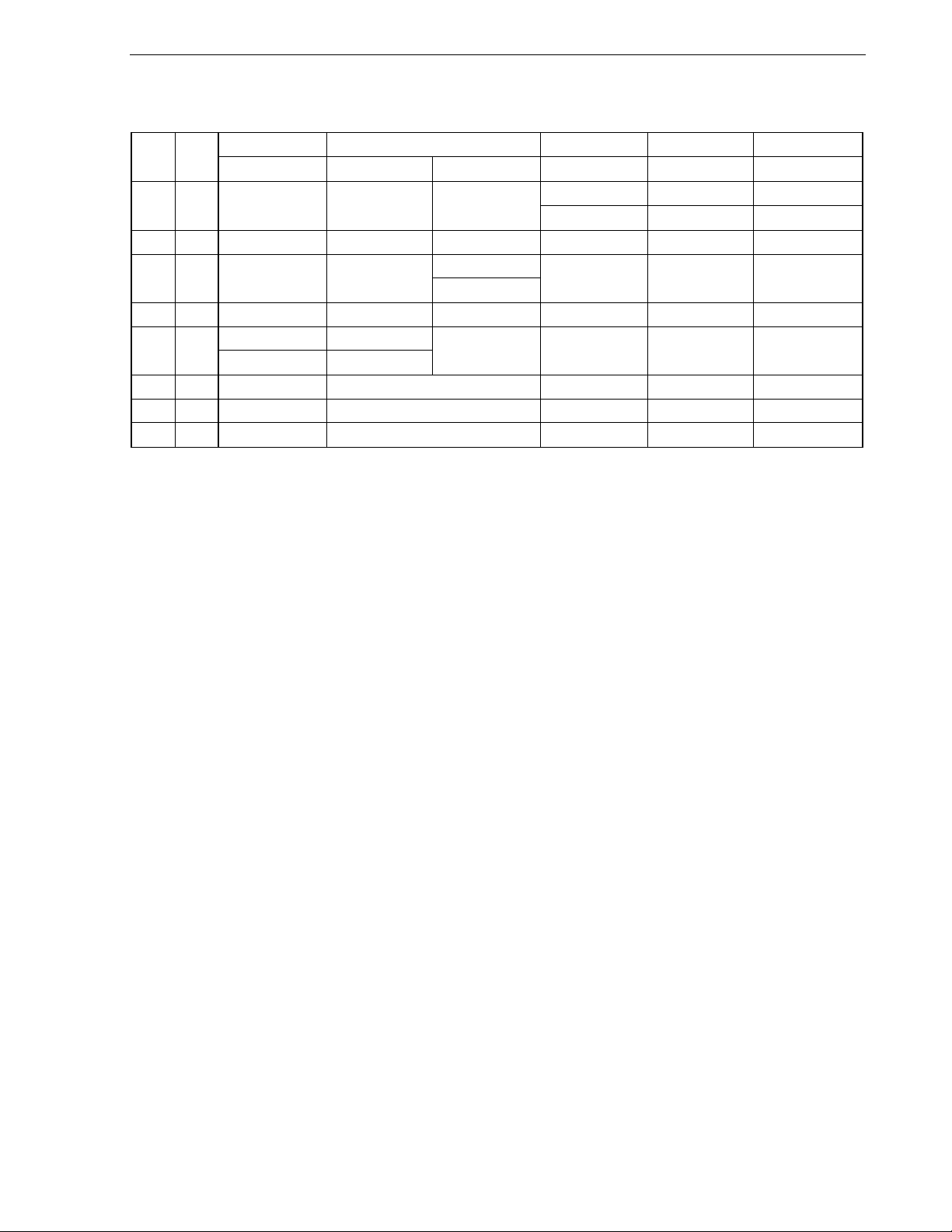
1.5 78K0/Kx2 Microcontroller Lineup
78K0/KB2 78K0/KC2 78K0/KD2 78K0/KE2 78K0/KF2 ROM RAM
30/36 Pins 38/44 Pins 48 Pins 52 Pins 64 Pins 80 Pins
128 KB 7 KB
96 KB 5 KB
60 KB 3 KB
48 KB 2 KB
32 KB 1 KB
24 KB 1 KB µPD78F0502
16 KB 768 B µPD78F0501
8 KB 512 B µPD78F0500
Note Product with on-chip debug function
− − −
− − −
− −
− −
µ
PD78F0503D
µ
PD78F0503
Note
µ
PD78F0513D
µ
PD78F0513
µ
µ
CHAPTER 1 OUTLINE
µ
PD78F0515D
µ
PD78F0515
µ
PD78F0514
Note
µ
PD78F0513
PD78F0512
PD78F0511
µ
Note
PD78F0527D
µ
PD78F0527
µ
PD78F0526
µ
PD78F0525
µ
PD78F0524
µ
PD78F0523
µ
PD78F0522
µ
PD78F0521
Note
µ
PD78F0537D
µ
PD78F0537
µ
PD78F0536
µ
PD78F0535
µ
PD78F0534
µ
PD78F0533
µ
PD78F0532
µ
PD78F0531
Note
µPD78F0547D
− − − −
µ
PD78F0547
µ
PD78F0546
µ
PD78F0545
µ
PD78F0544
−
−
−
Note
User’s Manual U17260EJ6V0UD
25

CHAPTER 1 OUTLINE
The list of functions in the 78K0/Kx2 microcontrollers is shown below.
(1/2)
78K0/KB2 78K0/KC2 Part Number
Item
30/36 Pins 38/44 Pins 48 Pins
Flash memory (KB) 8 16 24 32 16 24 32 16 24 32 48 60
RAM (KB) 0.5 0.75 1 1 0.75 1 1 0.75 1 1 2 3
Bank (flash memory)
Power supply voltage • Standard products, (A) grade products: VDD = 1.8 to 5.5 V
<R>
• (A2) grade products: V
−
DD = 2.7 to 5.5 V
Regulator Provided
Minimum instruction
execution time
0.1 µs (20 MHz: VDD = 4.0 to 5.5 V)/0.2 µs (10 MHz: VDD = 2.7 to 5.5 V)/
0.4
µ
s (5 MHz: VDD = 1.8 to 5.5 V)
High-speed system 20 MHz: VDD = 4.0 to 5.5 V/10 MHz: VDD = 2.7 to 5.5 V/5 MHz: VDD = 1.8 to 5.5 V
Internal high-speed
Main
oscillation
Clock
Subsystem
Internal low-speed
−
8 MHz (TYP.): VDD = 1.8 to 5.5 V
32.768 kHz (TYP.): VDD = 1.8 to 5.5 V
240 kHz (TYP.): VDD = 1.8 to 5.5 V
oscillation
Total 23 31 (38 pins)/
41
37 (44 pins)
Port
N-ch O.D. (6 V
2 4 4
tolerance)
16 bits (TM0) 1 ch
8 bits (TM5) 2 ch
8 bits (TMH) 2 ch
Timer
Watch
−
1 ch
WDT 1 ch
3-wire CSI
Automatic transmit/
−
−
receive 3-wire CSI
UART/3-wire CSI
UART supporting LIN-
Serial interface
bus
Note
1 ch
1 ch
I2C bus 1 ch
10-bit A/D 4 ch 6 ch (38 pins)/
8 ch
8 ch (44 pins)
External 6 7 8
Internal 14 16
Interrupt
Key interrupt
−
2 ch (38 pins)/
4 ch
4 ch (44 pins)
RESET pin Provided
POC 1.59 V ±0.15 V (rise time to 1.8 V: 3.6 ms (MAX.))
Reset
LVI The detection level of the supply voltage is selectable in 16 steps.
WDT Provided
Clock output/buzzer output
Multiplier/divider
On-chip debug function
Operating ambient
<R>
temperature
µ
PD78F0503D only
• Standard products, (A) grade products: TA = –40 to +85°C
• (A2) grade products: T
−
−
µ
PD78F0513D only
A = –40 to +110°C, TA = –40 to +125°C
Clock output only
µ
PD78F0515D only
Provided
Note Select either of the functions of these alternate-function pins.
26
User’s Manual U17260EJ6V0UD

<R>
<R>
CHAPTER 1 OUTLINE
(2/2)
78K0/KD2 78K0/KE2 78K0/KF2 Part Number
Item
52 Pins 64 Pins 80 Pins
Flash memory (KB) 16 24 32 48 60 96 128 16 24 32 48 60 96 128 48 60 96 128
RAM (KB) 0.75 1 1 2 3 5 7 0.75 1 1 2 3 5 7 2 3 5 7
Bank (flash memory)
−
4 6
−
4 6
−
4 6
Power supply voltage • Standard products, (A) grade products: VDD = 1.8 to 5.5 V
• (A2) grade products: V
DD = 2.7 to 5.5 V
Regulator Provided
Minimum instruction
execution time
0.1 µs (20 MHz: VDD = 4.0 to 5.5 V)/0.2 µs (10 MHz: VDD = 2.7 to 5.5 V)/
µ
s (5 MHz: VDD = 1.8 to 5.5 V)
0.4
High-speed system 20 MHz: VDD = 4.0 to 5.5 V/10 MHz: VDD = 2.7 to 5.5 V/5 MHz: VDD = 1.8 to 5.5 V
Internal high-speed
Main
oscillation
Clock
Subsystem 32.768 kHz (TYP.): VDD = 1.8 to 5.5 V
Internal low-speed
8 MHz (TYP.): VDD = 1.8 to 5.5 V
240 kHz (TYP.): VDD = 1.8 to 5.5 V
oscillation
Total 45 55 71
N-ch O.D. (6 V
Port
4 4 4
tolerance)
16 bits (TM0) 1 ch 2 ch
8 bits (TM5) 2 ch
8 bits (TMH) 2 ch
Timer
Watch 1 ch
WDT 1 ch
3-wire CSI
Automatic transmit/
−
−
1 ch
1 ch
receive 3-wire CSI
UART/3-wire CSI
UART supporting LIN-
Serial interface
bus
Note
1 ch
1 ch
I2C bus 1 ch
10-bit A/D 8 ch
External 8 9
Internal 16 19 20
Interrupt
Key interrupt 8 ch
RESET pin Provided
POC 1.59 V ±0.15 V (rise time to 1.8 V: 3.6 ms (MAX.))
Reset
LVI The detection level of the supply voltage is selectable in 16 steps.
WDT Provided
Clock output/buzzer output Clock output only Provided
Multiplier/divider
On-chip debug function
Operating ambient
temperature
−
µ
PD78F0527D only
Provided
−
µ
PD78F0537D only
Provided
• Standard products, (A) grade products: TA = –40 to +85°C
• (A2) grade products: T
A = –40 to +110°C, TA = –40 to +125°C
µ
PD78F0547D only
Note Select either of the functions of these alternate-function pins.
User’s Manual U17260EJ6V0UD
27

1.6 Block Diagram
TO00/TI010/P01
TI000/P00 (LINSEL)
RxD6/P14 (LINSEL)
TO01
Note2
/TI011
TI001
Note2
Note2
/P06
/P05
16-bit TIMER/
EVENT COUNTER 00
16-bit TIMER/
EVENT COUNTER 01
Note2
CHAPTER 1 OUTLINE
PORT 0
PORT 1
7
8
P00 to P06
P10 to P17
TOH0/P15
TOH1/P16
TI50/TO50/P17
TI51/TO51/P33
RxD0/P11
TxD0/P10
RxD6/P14
TxD6/P13
SI10/P11
SO10/P12
SCK10/P10
Note2
SI11
/P03
Note2
SO11
/P02
Note2
SCK11
SSI11
RxD6/P14 (LINSEL)
INTP0/P120(LINSEL)
/P04
Note2
/P05
EXSCL0/P62
SDA0/P61
SCL0/P60
ANI0/P20 to
ANI7/P27
AV
AV
INTP1/P30 to
INTP4/P33
INTP5/P16
INTP6/P140,
INTP7/P141
REF
SS
8-bit TIMER
8-bit TIMER
WATCHDOG TIMER
8-bit TIMER/
EVENT COUNTER 50
8-bit TIMER/
EVENT COUNTER 51
WATCH TIMER
SERIAL
INTERFACE UART0
SERIAL
INTERFACE UART6
SERIAL
INTERFACE CSI10
SERIAL INTERFACE
CSI11
SERIAL
INTERFACE IIC0
8
A/D CONVERTER
4
2
Notes 1. Available only in the
2. Available only in the
3. Available only in the
INTERNAL
LOW-SPEED
OSCILLATOR
LINSEL
Note2
INTERRUPT
CONTROL
H0
H1
78K/0
CPU
CORE
BANK
INTERNAL
HIGH-SPEED
RAM
EV
µ
PD78F0536, 78F0537, and 78F0537D.
µ
PD78F0534, 78F0535, 78F0536, 78F0537, and 78F0537D.
µ
PD78F0537D.
Note1
DD
VSS,
EV
MEMORY
SS
FLASH
INTERNAL
EXPANSION
Note2
RAM
FLMD0 VDD,
PORT 2
PORT 3
PORT 4
PORT 5
PORT 6
PORT 7
PORT 12
PORT 13 P130
PORT 14 P140, P141
BUZZER OUTPUT
CLOCK OUTPUT
CONTROL
POWER ON CLEAR/
LOW VOLTAGE
INDICATOR
KEY RETURN
RESET CONTROL
MULTIPLIER&
Note2
DIVIDER
ON-CHIP DEBUG
SYSTEM
CONTROL
INTERNAL
HIGH-SPEED
OSCILLATOR
VOLTAGE
REGULATOR
5
Note3
8
P20 to P27
4
P30 to P33
4
P40 to P43
4
P50 to P53
4
P60 to P63
8
P70 to P77
P120 to P124
2
BUZ/P141
PCL/P140
POC/LVI
CONTROL
KR0/P70 to
8
KR7/P77
Note3
OCD0A
Note3
OCD0B
RESET
X1/P121
X2/EXCLK/P122
XT1/P123
XT2/EXCLKS/P124
REGC
EXLVI/P120
/X1, OCD1A
/X2, OCD1B
Note3
Note3
/P31
/P32
28
User’s Manual U17260EJ6V0UD

<R>
<R>
<R>
<R>
CHAPTER 1 OUTLINE
1.7 Outline of Functions
(1/2)
Item
Internal
memory
Flash memory
(self-programming
supported)
Note 1
Memory bank
High-speed RAM
Expansion RAM
Note 1
Memory space 64 KB
Main
system
clock
(oscillation
frequency)
High-speed system
clock
Standard
products, (A)
grade products
(A2) grade
products
Internal high-speed
oscillation clock
Standard
products, (A)
grade products
(A2) grade
products
Subsystem clock (oscillation XT1 (crystal) oscillation, external subsystem clock input (EXCLKS)
frequency)
Standard
products, (A)
grade products
(A2) grade
products
Internal low-speed oscillation Internal oscillation
clock (for TMH1,
WDT)
Standard
products, (A)
grade products
(A2) grade
products
General-purpose registers 8 bits × 32 registers (8 bits × 8 registers × 4 banks)
Minimum instruction execution time
Instruction set • 8-bit operation, 16-bit operation
I/O ports
Notes 1. The internal flash memory capacity, internal high-speed RAM capacity, and internal expansion RAM
capacity can be changed using the internal memory size switching register (IMS) and the internal
expansion RAM size switching register (IXS).
2. Memory banks to be used can be changed using the bank select register (BANK).
µ
PD78F0531µPD78F0532µPD78F0533µPD78F0534µPD78F0535µPD78F0536 µPD78F0537µPD78F0537D
16 KB 24 KB 32 KB 48 KB 60 KB 96 KB 128 KB
Note 2
Note 1
768 bytes 1 KB
−
−
1 KB 2 KB 4 KB 6 KB
4 banks 6 banks
X1 (crystal/ceramic) oscillation, external main system clock input (EXCLK)
1 to 20 MHz: VDD = 4.0 to 5.5 V, 1 to 10 MHz: VDD = 2.7 to 5.5 V,
1 to 5 MHz: VDD = 1.8 to 5.5 V
1 to 20 MHz: V
DD = 4.0 to 5.5 V, 1 to 10 MHz: VDD = 2.7 to 5.5 V
Internal oscillation
8 MHz (TYP.): VDD = 1.8 to 5.5 V
8 MHz (TYP.): V
DD = 2.7 to 5.5 V
32.768 kHz (TYP.): VDD = 1.8 to 5.5 V
32.768 kHz (TYP.): V
DD = 2.7 to 5.5 V
240 kHz (TYP.): VDD = 1.8 to 5.5 V
240 kHz (TYP.): V
DD = 2.7 to 5.5 V
0.1 µs (high-speed system clock: @ fXH = 20 MHz operation)
0.25 µs (TYP.) (internal high-speed oscillation clock: @ fRH = 8 MHz (TYP.) operation)
122
µ
s (subsystem clock: @ fSUB = 32.768 kHz operation)
• Multiply/divide (8 bits × 8 bits, 16 bits ÷ 8 bits)
• Bit manipulate (set, reset, test, and Boolean operation)
• BCD adjust, etc.
Total: 55
CMOS I/O: 50
CMOS output: 1
N-ch open-drain I/O (6 V tolerance): 4
User’s Manual U17260EJ6V0UD
29

CHAPTER 1 OUTLINE
Item
Timers • 16-bit timer/event counter: 1
µ
PD78F0531 µPD78F0532µPD78F0533µPD78F0534µPD78F0535µPD78F0536 µPD78F0537 µPD78F0537D
• 16-bit timer/event counter: 2 channels
channel
• 8-bit timer/event counter: 2
channels
• 8-bit timer: 2 channels
• 8-bit timer/event counter: 2 channels
• 8-bit timer: 2 channels
• Watch timer: 1 channel
• Watchdog timer: 1 channel
• Watch timer: 1 channel
• Watchdog timer: 1 channel
Timer outputs 5 (PWM output: 4, PPG output: 1) 6 (PWM output: 4, PPG output: 2)
Clock output • 156.25 kHz, 312.5 kHz, 625 kHz, 1.25 MHz, 2.5 MHz, 5 MHz, 10 MHz
(peripheral hardware clock: @ f
• 32.768 kHz (subsystem clock: @ f
PRS = 20 MHz operation)
SUB = 32.768 kHz operation)
Buzzer output 2.44 kHz, 4.88 kHz, 9.77 kHz, 19.54 kHz
(peripheral hardware clock: @ f
PRS = 20 MHz operation)
A/D converter 10-bit resolution × 8 channels (AVREF = 2.3 to 5.5 V)
Serial interface • UART mode supporting LIN-
bus: 1 channel
• 3-wire serial I/O mode/UART
Note
: 1 channel
mode
2
• I
C bus mode: 1 channel
Multiplier/divider
−
• UART mode supporting LIN-bus: 1 channel
• 3-wire serial I/O mode/UART mode
• 3-wire serial I/O mode: 1 channel
2
C bus mode: 1 channel
• I
Note
: 1 channel
• 16 bits × 16 bits = 32 bits (multiplication)
• 32 bits ÷ 16 bits = 32 bits remainder of 16 bits
(division)
Internal 16 19 Vectored
interrupt sources
External 9
Key interrupt Key interrupt (INTKR) occurs by detecting falling edge of key input pins (KR0 to KR7).
Reset • Reset using RESET pin
• Internal reset by watchdog timer
• Internal reset by power-on-clear
• Internal reset by low-voltage detector
On-chip debug function None Provided
<R>
Power supply voltage • Standard products, (A) grade products: VDD = 1.8 to 5.5 V
• (A2) grade products: V
Operating ambient temperature • Standard products, (A) grade products: TA = –40 to +85°C
<R>
• (A2) grade products: T
DD = 2.7 to 5.5 V
A = –40 to +110°C, TA = –40 to +125°C
Package • 64-pin plastic LQFP (fine pitch) (10 × 10)
• 64-pin plastic LQFP (14 × 14)
• 64-pin plastic LQFP (12 × 12)
• 64-pin plastic TQFP (fine pitch) (7 × 7)
• 64-pin plastic FLGA (5 × 5)
Note Select either of the functions of these alternate-function pins.
(2/2)
30
User’s Manual U17260EJ6V0UD
 Loading...