

Page 1
MM54HC149/MM74HC149
8 Line to 8 Line Priority Encoder
MM54HC149/MM74HC149 8 Line to 8 Line Priority Encoder
January 1988
General Description
This priority encoder utilizes advanced silicon-gate CMOS
technology. It has the high noise immunity and low power
consumption typical of CMOS circuits, as well as the speeds
and output drive similar to LS-TTL.
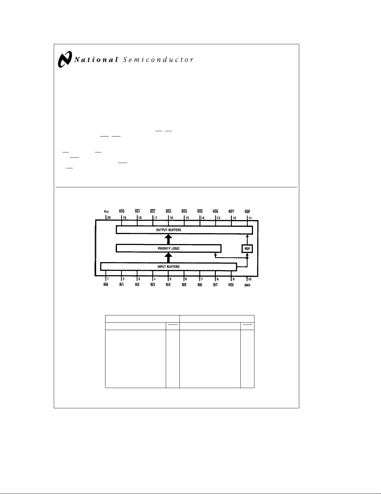
This priority encoder accepts 8 input request lines, RI7
and outputs 8 lines, RO7
can be low at a time. The output that is low is dependent on
the highest priority request that is low. The order of priority
is RI7
highest and RI0 lowest. Also provided is and enable
input, RQE
quest output is also provided, RQP
any RIn
All inputs to this device are protected from damage due to
electrostatic discharge by diodes to V
, which when high forces all outputs high. A re-
is active.
–RO0. Only one request output
, which goes low when
and ground.
CC
–RI0,
Connection Diagram
Dual-In-Line Package
Features
Y
Propagation delay: 15 ns typical
Y
Wide power supply range: 2– 6V
Y
Low quiescent current: 80 mA max (74HC Series)
Y
Wide input noise immunity
Top View
Order Number MM54HC149 or MM74HC149
TL/F/5312– 1
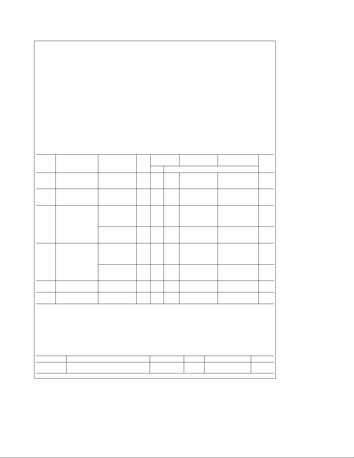
Truth Table
Inputs Outputs
01234567RQE01234567RQP
XXXXXXXX H HHHHHHHH H
HHHHHHHH L HHHHHHHH H
XXXXXXXL L HHHHHHHL L
XXXXXXLH L HHHHHHLH L
XXXXXLHH L HHHHHLHH L
XXXXLHHH L HHHHLHHH L
XX X L HHHH L HHH LHHHH L
XX LHHHHH L HHLHHHHH L
X LHHHHHH L HL HHHHHH L
LHHHHHHH L LHHHHHHH L
C
1995 National Semiconductor Corporation RRD-B30M105/Printed in U. S. A.
TL/F/5312
Page 2
Absolute Maximum Ratings (Notes1&2)
Operating Conditions
If Military/Aerospace specified devices are required,
please contact the National Semiconductor Sales
Office/Distributors for availability and specifications.
Supply Voltage (V
CC
)
DC Input Voltage (VIN)
DC Output Voltage (V
OUT
)
Clamp Diode Current (IIK,IOK)
DC Output Current, per pin (I
OUT
)
DC VCCor GND Current, per pin (ICC)
Storage Temperature Range (T
STG
b
b
)
b
0.5 toa7.0V
1.5 to V
CC
0.5 to V
CC
g
g
b
g
65§Ctoa150§C
a
1.5V
a
0.5V
20 mA
25 mA
50 mA
Supply Voltage (V
)26V
CC
DC Input or Output Voltage 0 V
(V
IN,VOUT
)
Operating Temp. Range (TA)
MM74HC
MM54HC
Input Rise or Fall Times
e
V
2.0V(tr,tf) 1000 ns
CC
e
V
4.5V 500 ns
CC
e
V
6.0V 400 ns
CC
Power Dissipation (PD)
(Note 3) 600 mW
S.O. Package only 500 mW
Lead Temperature (T
)
L
(Soldering 10 seconds) 260§C
DC Electrical Characteristics (Note 4)
Symbol Parameter Conditions V
CC
A
e
T
25§C
Typ Guaranteed Limits
V
IH
Minimum High Level 2.0V 1.5 1.5 1.5 V
Input Voltage 4.5V 3.15 3.15 3.15 V
6.0V 4.2 4.2 4.2 V
V
IL
Maximum Low Level 2.0V 0.5 0.5 0.5 V
Input Voltage** 4.5V 1.35 1.35 1.35 V
6.0V 1.8 1.8 1.8 V
V
OH
Minimum High Level V
Output Voltage
e
VIHor V
l
I
IN
OUT
IL
s
20 mA 2.0V 2.0 1.9 1.9 1.9 V
l
4.5V 4.5 4.4 4.4 4.4 V
6.0V 6.0 5.9 5.9 5.9 V
e
V
VIHor V
IN
I
l
OUT
I
l
OUT
V
OL
Maximum Low Level V
Output Voltage
l
I
IN
OUT
e
IL
s
4.0 mA 4.5V 4.2 3.98 3.84 3.7 V
l
s
5.2 mA 6.0V 5.7 5.48 5.34 5.2 V
l
VIHor V
IL
s
20 mA 2.0V 0 0.1 0.1 0.1 V
l
4.5V 0 0.1 0.1 0.1 V
6.0V 0 0.1 0.1 0.1 V
e
V
VIHor V
IN
I
l
OUT
I
l
OUT
I
IN
I
CC
Note 1: Absolute Maximum Ratings are those values beyond which damage to the device may occur.
Note 2: Unless otherwise specified all voltages are referenced to ground.
Note 3: Power Dissipation temperature derating Ð plastic ‘‘N’’ package:
Note 4: For a power supply of 5V
with this supply. Worst case V
I
**V
Maximum Input V
Current
Maximum Quiescent V
Supply Current I
g
and VILoccur at V
) occur for CMOS at the higher voltage and so the 6.0V values should be used.
OZ
limits are currently tested at 20% of VCC. The above VILspecification (30% of VCC) will be implemented no later than Q1, CY’89.
IL
IH
e
IN
e
IN
OUT
10% the worst case output voltages (VOH, and VOL) occur for HC at 4.5V. Thus the 4.5V values should be used when designing
IL
s
4.0 mA 4.5V 0.2 0.26 0.33 0.4 V
l
s
5.2 mA 6.0V 0.2 0.26 0.33 0.4 V
l
VCCor GND 6.0V
VCCor GND 6.0V 8.0 80 160 mA
e
0 mA
b
12 mW/§C from 65§Cto85§C; ceramic ‘‘J’’ package:b12 mW/§C from 100§Cto125§C.
e
5.5V and 4.5V respectively. (The VIHvalue at 5.5V is 3.85V.) The worst case leakage current (IIN,ICC, and
CC
g
0.1
74HC 54HC
eb
T
40 to 85§CT
A
g
1.0
Min Max Units
V
§
§
Units
b
b
40
55
eb
A
55 to 125§C
g
CC
a
85
a
125
1.0 mA
C
C
AC Electrical Characteristics V
CC
5V, T
e
A
25§C, C
e
L
15 pF, t
e
t
r
f
e
6 ns (Note 6)
e
Symbol Parameter Conditions Typ Guaranteed Limit Units
t
PHL,tPLH
Maximum Propagation Delay, Any Input
To Any Output 20 33 ns
2
Page 3

AC Electrical Characteristics V
CC
Symbol Parameter Conditions V
t
PHL,tPLH
t
TLH,tTHL
C
PD
C
IN
Note 5: CPDdetermines the no load dynamic power consumption, P
Maximum Propagation 2.0V 73 205 255 310 ns
Delay Any Input To Any 4.5V 25 41 51 62 ns
Output 6.0V 21 35 43 53 ns
Maximum Output Rise 2.0V 30 75 95 110 ns
and Fall Time 4.5V 8 15 19 22 ns
Power Dissipation 50 pF
Capacitance (Note 5)
Maximum Input 7 10 10 10 pF
Capacitance
Simplified Logic Diagram
e
2.0V to 6.0V, C
CC
e
L
e
T
25§C
A
50 pF, t
T
e
e
t
6 ns (unless otherwise specified)
r
f
74HC 54HC
eb
40 to 85§CT
A
eb
A
55 to 125§C
Typ Guaranteed Limits
6.0V 7 13 16 19 ns
2
e
CPDV
D
faICCVCC, and the no load dynamic current consumption, I
CC
e
CPDVCCfaICC.
S
Units
TL/F/5312– 2
3
Page 4

Physical Dimensions inches (millimeters)
Ceramic Dual-In-Line Package (J)
Order Number MM54HC149J or MM74HC149J
NS Package J20A
MM54HC149/MM74HC149 8 Line to 8 Line Priority Encoder
Molded Dual-In-Line Package (N)
Order Number MM74HC149N
LIFE SUPPORT POLICY
NATIONAL’S PRODUCTS ARE NOT AUTHORIZED FOR USE AS CRITICAL COMPONENTS IN LIFE SUPPORT
DEVICES OR SYSTEMS WITHOUT THE EXPRESS WRITTEN APPROVAL OF THE PRESIDENT OF NATIONAL
SEMICONDUCTOR CORPORATION. As used herein:
1. Life support devices or systems are devices or 2. A critical component is any component of a life
systems which, (a) are intended for surgical implant support device or system whose failure to perform can
into the body, or (b) support or sustain life, and whose be reasonably expected to cause the failure of the life
failure to perform, when properly used in accordance support device or system, or to affect its safety or
with instructions for use provided in the labeling, can effectiveness.
be reasonably expected to result in a significant injury
to the user.
National Semiconductor National Semiconductor National Semiconductor National Semiconductor
Corporation Europe Hong Kong Ltd. Japan Ltd.
1111 West Bardin Road Fax: (
Arlington, TX 76017 Email: cnjwge@tevm2.nsc.com Ocean Centre, 5 Canton Rd. Fax: 81-043-299-2408
Tel: 1(800) 272-9959 Deutsch Tel: (
Fax: 1(800) 737-7018 English Tel: (
National does not assume any responsibility for use of any circuitry described, no circuit patent licenses are implied and National reserves the right at any time without notice to change said circuitry and specifications.
Fran3ais Tel: (
Italiano Tel: (
NS Package N20A
a
49) 0-180-530 85 86 13th Floor, Straight Block, Tel: 81-043-299-2309
a
49) 0-180-530 85 85 Tsimshatsui, Kowloon
a
49) 0-180-532 78 32 Hong Kong
a
49) 0-180-532 93 58 Tel: (852) 2737-1600
a
49) 0-180-534 16 80 Fax: (852) 2736-9960
 Loading...