

National Semiconductor MM54HC373, MM74HC373 Service Manual
MM54HC373/MM74HC373
TRI-STATE
General Description
These high speed octal D-type latches utilize advanced silicon-gate CMOS technology. They possess the high noise
immunity and low power consumption of standard CMOS
integrated circuits, as well as the ability to drive 15 LS-TTL
loads. Due to the large output drive capability and the TRISTATE feature, these devices are ideally suited for interfacing with bus lines in a bus organized system.
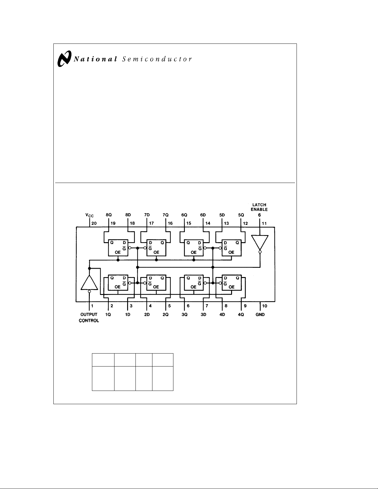
When the LATCH ENABLE input is high, the Q outputs will
follow the D inputs. When the LATCH ENABLE goes low,
data at the D inputs will be retained at the outputs until
LATCH ENABLE returns high again. When a high logic level
is applied to the OUTPUT CONTROL input, all outputs go to
a high impedance state, regardless of what signals are pres-
Connection Diagram
Octal D-Type Latch
É
Dual-In-Line Package
January 1988
ent at the other inputs and the state of the storage elements.
The 54HC/74HC logic family is speed, function, and pin-out
compatible with the standard 54LS/74LS logic family. All
inputs are protected from damage due to static discharge by
internal diode clamps to V
and ground.
CC
Features
Y
Typical propagation delay: 18 ns
Y
Wide operating voltage range: 2 to 6 volts
Y
Low input current: 1 mA maximum
Y
Low quiescent current: 80 mA maximum (74 Series)
Y
Output drive capability: 15 LS-TTL loads
MM54HC373/MM74HC373 TRI-STATE Octal D-Type Latch
Top View
Order Number MM54HC373 or MM74HC373
TL/F/5335– 1
Truth Table
Output Latch
Control Enable Output
LHHH
LHLL
LLXQ
HXXZ
TRI-STATEÉis a registered trademark of National Semiconductor Corporation.
C
1995 National Semiconductor Corporation RRD-B30M105/Printed in U. S. A.
TL/F/5335
Data
373
0
e
H
high level, Lelow level
e
Q
level of output before steady-state input
0
conditions were established.
e
Z
high impedance
Absolute Maximum Ratings (Notes1&2)
Operating Conditions
If Military/Aerospace specified devices are required,
please contact the National Semiconductor Sales
Office/Distributors for availability and specifications.
)
b
0.5 toa7.0V
b
1.5 to V
CC
b
0.5 to V
CC
b
65§Ctoa150§C
a
a
g
g
g
1.5V
0.5V
20 mA
35 mA
70 mA
Supply Voltage (V
CC
)
DC Input Voltage (VIN)
DC Output Voltage (V
OUT
)
Clamp Diode Current (IIK,IOK)
DC Output Current, per pin (I
OUT
)
DC VCCor GND Current, per pin (ICC)
Storage Temperature Range (T
STG
Supply Voltage (V
)26V
CC
DC Input or Output Voltage 0 V
(V
IN,VOUT
)
Operating Temp. Range (TA)
MM74HC
MM54HC
Input Rise or Fall Times
e
V
2.0V(tr,tf) 1000 ns
CC
e
V
4.5V 500 ns
CC
e
V
6.0V 400 ns
CC
Power Dissipation (PD)
(Note 3) 600 mW
S.O. Package only 500 mW
Lead Temp. (T
) (Soldering 10 seconds) 260§C
L
DC Electrical Characteristics
e
T
25§C
Symbol Parameter Conditions V
CC
A
Typ Guaranteed Limits
V
Minimum High Level 2.0V 1.5 1.5 1.5 V
IH
Input Voltage 4.5V 3.15 3.15 3.15 V
6.0V 4.2 4.2 4.2 V
V
Maximum Low Level 2.0V 0.5 0.5 0.5 V
IL
Input Voltage** 4.5V 1.35 1.35 1.35 V
6.0V 1.8 1.8 1.8 V
V
Minimum High Level V
OH
Output Voltage
e
VIHor V
l
IN
I
OUT
IL
s
20 mA 2.0V 2.0 1.9 1.9 1.9 V
l
4.5V 4.5 4.4 4.4 4.4 V
6.0V 6.0 5.9 5.9 5.9 V
e
V
VIHor V
IN
I
l
OUT
I
l
OUT
l
IN
I
OUT
e
V
Maximum Low Level V
OL
Output Voltage
IL
s
6.0 mA 4.5V 4.2 3.98 3.84 3.7 V
l
s
7.8 mA 6.0V 5.7 5.48 5.34 5.2 V
l
VIHor V
IL
s
20 mA 2.0V 0 0.1 0.1 0.1 V
l
4.5V 0 0.1 0.1 0.1 V
6.0V 0 0.1 0.1 0.1 V
e
V
VIHor V
IN
I
l
OUT
I
l
OUT
I
I
Maximum Input V
IN
Current
Maximum TRI-STATE V
OZ
Output Leakage V
Current
I
Maximum Quiescent V
CC
Supply Current I
Note 1: Absolute Maximum Ratings are those values beyond which damage to the device may occur.
Note 2: Unless otherwise specified all voltages are referenced to ground.
Note 3: Power Dissipation temperature derating Ð plastic ‘‘N’’ package:
Note 4: For a power supply of 5V
designing with this supply. Worst case V
, and IOZ) occur for CMOS at the higher voltage and so the 6.0V values should be used.
I
CC
**V
limits are currently tested at 20% of VCC. The above VILspecification (30% of VCC) will be implemented no later than Q1, CY’89.
IL
e
IN
e
IN
OUT
e
IN
OUT
g
10% the worst case output voltages (VOH, and VOL) occur for HC at 4.5V. Thus the 4.5V values should be used when
and VILoccur at V
IH
IL
s
6.0 mA 4.5V 0.2 0.26 0.33 0.4 V
l
s
7.8 mA 6.0V 0.2 0.26 0.33 0.4 V
l
VCCor GND 6.0V
VIHor VIL,OCeVIH6.0V
e
VCCor GND
g
0.1
g
0.5
VCCor GND 6.0V 8.0 80 160 mA
e
0 mA
b
12 mW/§C from 65§Cto85§C; ceramic ‘‘J’’ package:b12 mW/§C from 100§Cto125§C.
e
5.5V and 4.5V respectively. (The VIHvalue at 5.5V is 3.85V.) The worst case leakage current (IIN,
CC
74HC 54HC
eb
T
40 to 85§CT
A
g
1.0
g
5
Min Max Units
CC
b
b
40
55
eb
A
a
85
a
125
55 to 125§C
g
1.0 mA
g
10 mA
V
§
§
Units
C
C
2
 Loading...