

Page 1
MM54HC299/MM74HC299
8-Bit TRI-STATE
General Description
This 8-bit TRI-STATE shift/storage register utilizes advanced
silicon-gate CMOS technology. Along with the low power
consumption and high noise immunity of standard CMOS
integrated circuits, it has the ability to drive 15 LS-TTL
loads. This circuit also features operating speeds comparable to the equivalent low power Schottky device.
The MM54HC299/MM74HC299 features multiplexed inputs/outputs to achieve full 8-bit data handling in a single
20-pin package. Due to the large output drive capability and
TRI-STATE feature, this device is ideally suited for interfacing with bus lines in a bus oriented system.
Two function select inputs and two output control inputs are
used to choose the mode of operation as listed in the function table. Synchronous parallel loading is accomplished by
taking both function select lines S0 and S1 high. This places
the TRI-STATE outputs in a high impedance state, which
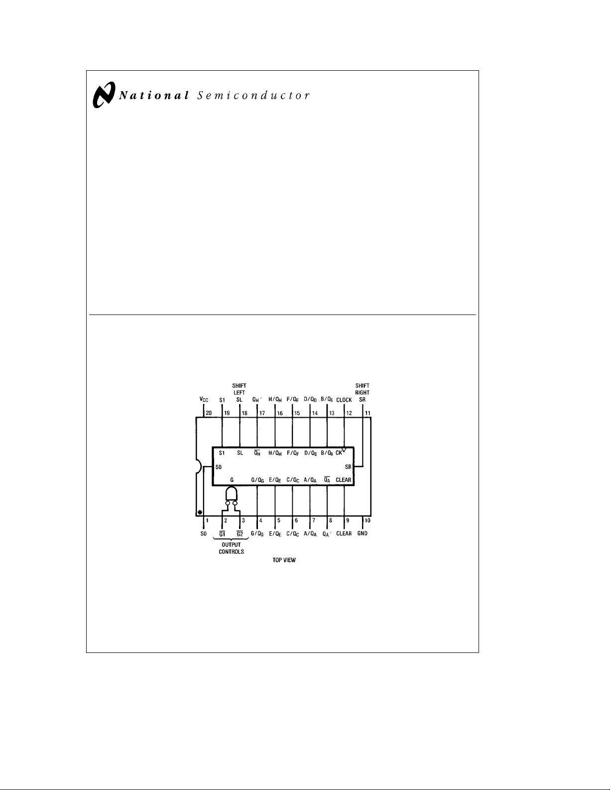
Connection Diagram
Universal Shift Register
É
January 1988
permits data applied to the input/output lines to be clocked
into the register. Reading out of the register can be done
while the outputs are enabled in any mode. A direct overriding CLEAR input is provided to clear the register whether
the outputs are enabled or disabled.
The 54HC/74HC logic family is functionally as well as pinout
compatible with the standard 54LS/74LS logic family. All
inputs are protected from damage due to static discharge by
internal diode clamps to V
and ground.
CC
Features
Y
Typical operating frequency 40 MHz
Y
Typical propagation delay: 20 ns
Y
Low quiescent current: 80 mA maximum (74HC)
Y
High output drive for bus applications
Y
Low quiescent current: 1 mA maximum
MM54HC299/MM74HC299 8-Bit TRI-STATE Universal Shift Register
Dual-In-Line Package
TL/F/5207– 1
Order Number MM54HC299 or MM74HC299
TRI-STATEÉis a registered trademark of National Semiconductor Corporation.
C
1995 National Semiconductor Corporation RRD-B30M105/Printed in U. S. A.
TL/F/5207
Page 2
Absolute Maximum Ratings (Notes1&2)
Operating Conditions
If Military/Aerospace specified devices are required,
please contact the National Semiconductor Sales
Office/Distributors for availability and specifications.
Supply Voltage (V
DC Input Voltage (V
DC Output Voltage (V
Clamp Diode Current (I
DC Output Current, per pin (I
DC V
or GND Current, per pin (ICC)
CC
Storage Temperature Range (T
Power Dissipation (P
(Note 3) 600 mW
CC
)
)
IN
)
OUT
)
CD
)
OUT
STG
)
D
b
b
g
b
)
b
0.5 toa7.0V
CC
CC
a
a
g
1.5V
0.5V
20 mA
1.5 to V
0.5 to V
25 mA (QA’,QH’)
g
35 mA (others)
g
70 mA
65§Ctoa150§C
Supply Voltage (V
)26V
CC
DC Input or Output Voltage 0 V
(V
IN,VOUT
)
Operating Temp. Range (T
MM74HC
MM54HC
Input Rise or Fall Times
e
V
2.0V(tr,tf) 1000 ns
CC
e
V
4.5V 500 ns
CC
e
V
6.0V 400 ns
CC
S.O. Package only 500 mW
Lead Temp. (T
) (Soldering 10 seconds) 260§C
L
DC Electrical Characteristics (Note 4)
e
T
25§C
Symbol Parameter Conditions V
CC
A
Typ Guaranteed Limits
V
Minimum High Level Input 2.0V 1.5 1.5 1.5 V
IH
Voltage 4.5V 3.15 3.15 3.15 V
6.0V 4.2 4.2 4.2 V
V
Maximum Low Level Input 2.0V 0.5 0.5 0.5 V
IL
Voltage** 4.5V 1.35 1.35 1.35 V
6.0V 1.8 1.8 1.8 V
V
Minimum High Level V
OH
Output Voltage
e
VIHor V
l
I
OUT
IN
IL
s
20 mA 2.0V 2.0 1.9 1.9 1.9 V
l
4.5V 4.5 4.4 4.4 4.4 V
6.0V 6.0 5.9 5.9 5.9 V
QA'&QH'Outputs V
A/QAthru H/QHOutputs V
V
Maximum Low Level V
OL
Output Voltage
e
VIHor V
l
l
l
l
l
I
OUT
I
OUT
I
OUT
I
OUT
I
OUT
IN
e
IN
e
IN
IL
s
4.0 mA 4.5V 4.2 3.98 3.84 3.7 V
l
s
5.2 mA 6.0V 5.7 5.48 5.34 5.2 V
l
VIHor V
IL
s
6.0 mA 4.5V 4.2 3.98 3.84 3.7 V
l
s
7.8 mA 6.0V 5.7 5.48 5.34 5.2 V
l
VIHor V
IL
s
20 mA 2.0V 0 0.1 0.1 0.1 V
l
4.5V 0 0.1 0.1 0.1 V
6.0V 0 0.1 0.1 0.1 V
QA'and QH'Outputs V
A/QAthru H/QHOutputs V
I
I
Maximum Input Current V
IN
Maximum TRI-STATE Output V
OZ
Leakage Currrent GeV
I
Maximum Quiescent Supply V
CC
Current I
Note 1: Absolute Maximum Ratings are those values beyond which damage to the device may occur.
Note 2: Unless otherwise specified all voltages are referenced to ground.
Note 3: Power Dissipation temperature derating Ð plastic ‘‘N’’ package:
Note 4: For a power supply of 5V
designing with this supply. Worst-case V
, and IOZ) occur for CMOS at the higher voltage and so the 6.0V values should be used.
I
CC
limits are currently tested at 20% of VCC. The above VILspecification (30% of VCC) will be implemented no later than Q1, CY’89.
** V
IL
g
10% the worst-case output voltages (VOH, and VOL) occur for HC at 4.5V. Thus the 4.5V values should be used when
and VILoccur at V
IH
e
VIHor V
IN
I
l
OUT
I
l
OUT
IN
I
l
OUT
I
l
OUT
IN
OUT
GND
IN
OUT
e
e
e
IL
s
4 mA 4.5V 0.2 0.26 0.33 0.4 V
l
s
5.2 mA 6.0V 0.2 0.26 0.33 0.4 V
l
VIHor V
IL
s
6 mA 4.5V 0.2 0.26 0.33 0.4 V
l
s
7.8 mA 6.0V 0.2 0.26 0.33 0.4 V
l
VCCor GND 6.0V
e
VCCor 6.0V
IH
VCCor GND 6.0V 8.0 80 160 mA
e
0 mA
b
12 mW/§C from 65§Cto85§C; ceramic ‘‘J’’ package:b12 mW/§C from 100§Cto125§C.
e
5.5V and 4.5V respectively. (The VIHvalue at 5.5V is 3.85V.) The worst-case leakage current (IIN,
CC
g
0.1
g
0.5
74HC 54HC
eb
T
40 to 85§CT
A
g
1.0
g
0.5
Min Max Units
)
A
b
b
40
55
eb
A
a
a
55 to 125§C
g
1.0 mA
g
1.0 mA
CC
85
125
V
C
§
C
§
Units
V
V
V
V
2
Page 3

e
AC Electrical Characteristics V
CC
5V, T
A
e
25§C, t
Symbol Parameter Conditions Typ
f
MAX
t
PHL,tPLH
t
PHL
t
PHL,tPLH
t
PHL
t
PZL,tPZH
t
PHZ,tPLZ
t
S
t
H
t
W
t
REM
Maximum Operating 40 25 MHz
Frequency
Maximum Propagation 25 35 ns
Delay, Clock to Q
or Q
A'
H'
Maximum Propagation 39 40 ns
Delay, Clear to Q
Maximum Propagation C
Delay, Clock to Q
Maximum Propagation C
Delay, Clear to Q
Maximum Enable Time C
Maximum Disable Time C
or Q
A'
A±QH
A±QH
H'
e
45 pF 25 35 ns
L
e
45 pF 28 40 ns
L
e
45 pF 10 35 ns
L
e
R
1kX
L
e
5pF 18 25 ns
L
e
R
1kX
L
Minimum Setup Select 20 ns
Time
Data 20 ns
Minimum Hold Select 0 ns
Time
Data 0 ns
Minimum Pulse Width 12 20 ns
Clear Removal Time 10 ns
e
e
t
r
f
6 ns, C
Guaranteed
e
L
Limit
45 pF
Units
AC Electrical Characteristics C
e
L
50 pF, t
Symbol Parameter Conditions V
f
MAX
t
PHL,tPLH
t
PHL
t
PHL,tPLH
t
PHL
Maximum Operating Frequency 2.0V 5 4 3.5 MHz
Maximum Propagation 2.0V 15 170 210 240 ns
Delay, Clock to Q
or Q
A'
H'
Maximum Propagation 2.0V 70 200 250 280 ns
Delay, Clear to Q
Maximum Propagation C
Delay, Clock to QA±Q
Maximum Propagation C
Delay, Clear to QA±Q
or Q
A'
H'
e
50 pF 2.0V 65 170 210 240 ns
L
e
C
H
H
150 pF 2.0V 100 206 260 295 ns
L
e
C
50 pF 4.5V 27 38 48 54 ns
L
e
C
150 pF 4.5V 34 46 57 66 ns
L
e
C
50 pF 6.0V 25 35 44 49 ns
L
e
C
150 pF 6.0V 31 39 49 55 ns
L
e
50 pF 2.0V 70 200 250 280 ns
L
e
C
150 pF 2.0V 110 236 295 325 ns
L
e
C
50 pF 4.5V 30 44 55 62 ns
L
e
C
150 pF 4.5V 37 52 65 75 ns
L
e
C
50 pF 6.0V 26 38 46 52 ns
L
e
C
150 pF 6.0V 32 46 57 64 ns
L
e
e
t
6 ns unless otherwise specified
r
f
74HC 54HC
eb
T
40 to 85§CT
A
A
eb
55 to 125§C
Units
CC
e
T
25§C
A
Typ Guaranteed Limits
4.5V 25 20 18 MHz
6.0V 29 23 20 MHz
4.5V 27 38 48 54 ns
6.0V 25 35 44 49 ns
4.5V 30 44 55 62 ns
6.0V 26 38 46 52 ns
3
Page 4

AC Electrical Characteristic (Continued) C
Symbol Parameter Conditions V
t
PZH,tPZL
t
PHZ,tPLZ
t
S
t
H
t
REM
t
W
tr,t
t
THL,tTLH
C
C
C
Note 5: CPDdetermines the no load dynamic power consumption, P
I
S
Maximum Output Enable R
Maximum Output Disable Time R
Minimum Setup Time, 2.0V 100 125 140 ns
Data Select S
Minimum Hold Time, 2.0V 0 0 0 ns
Data Select SLor S
L
or S
R
R
Minimum Clear Removal Time 2.0V 10 10 10 ns
Minimum Pulse Width, 2.0V 100 125 140 ns
Clock and Clear 4.5V 20 25 28 ns
Maximum Input Rise 2.0V 1000 1000 100 ns
f
and Fall Time 4.5V 500 500 500 ns
Maximum Output Rise 2.0V 60 75 90 ns
and Fall Time, Clock 4.5V 12 15 18 ns
Power Dissipation Outputs Enabled 240 pF
PD
Capacitance Outputs Disabled 110 pF
Maximum Input Capacitance 5 10 10 10 pF
IN
Capacitance
Maximum TRI-STATE 15 20 20 20 pF
OUT
Output Capacitance
e
CPDVCCfaICC.
e
1kX
L
e
C
50 pF 2.0V 70 160 200 225 ns
L
e
150 pF 2.0V 90 220 275 310 ns
C
L
e
C
50 pF 4.5V 22 32 40 45 ns
L
e
C
150 pF 4.5V 30 44 55 62 ns
L
e
C
50 pF 6.0V 19 28 34 38 ns
L
e
C
150 pF 6.0V 24 47 47 51 ns
L
e
1kX 2.0V 70 160 200 225 ns
L
e
50 pF 4.5V 22 32 40 45 ns
C
L
e
L
CC
50 pF, t
T
A
e
e
t
6 ns unless otherwise specified
r
f
e
25§C
74HC 54HC
eb
T
40 to 85§CT
A
A
eb
55 to 125§C
Units
Typ Guaranteed Limits
6.0V 19 28 34 38 ns
4.5V 20 25 28 ns
6.0V 17 21 25 ns
4.5V 0 0 0 ns
6.0V 0 0 0 ns
4.5V 10 10 10 ns
6.0V 10 10 10 ns
6.0V 17 21 25 ns
6.0V 400 400 400 ns
6.0V 10 13 15 ns
2
e
CPDV
D
faICCVCC, and the no load dynamic current consumption,
CC
Function Table
Inputs Inputs/Outputs Outputs
Mode Clear Select Control Clock Serial A/Q
Clear
Hold
Shift Right
Shift Left
Load H H H X X
²
When one or both controls are high the eight input/output terminals are disabled to the high-impedance state; however, sequential operation or clearing of
the register is not affected.
Function Output
S1 S0 G1²G2
LXLLL XXXL L L L L L L LLL
LLXLL XXXL L L L L L L LLL
HLLLL XXXQ
HXXLLLorHXXQA0QB0QC0QD0QE0QF0QG0QH0QA0Q
HLHLL
HLHLL
HHLLL
HHLLL
²
SL SR
XH H QAnQBnQCnQDnQEnQFnQGnHQ
u
XL L QAnQBnQCnQDnQEnQFnQGnLQ
u
HX QBnQCnQDnQEnQFnQGnQ
u
LXQBnQCnQDnQEnQFnQGnQ
u
XX a b c d e f g h a h
u
B/QBC/QCD/QDE/QEF/QFG/QGH/QHQA’Q
A
A0QB0QC0QD0QE0QF0QG0QH0QA0QH0
HQBnH
Hn
LQBnL
Hn
4
H0
GN
GN
H’
Page 5

Logic Diagram
TL/F/5207– 2
5
Page 6

Physical Dimensions inches (millimeters)
Order Number MM54HC299J or MM74HC299J
NS Package J20A
MM54HC299/MM74HC299 8-Bit TRI-STATE Universal Shift Register
LIFE SUPPORT POLICY
Order Number MM74HC299N
NS Package N20A
NATIONAL’S PRODUCTS ARE NOT AUTHORIZED FOR USE AS CRITICAL COMPONENTS IN LIFE SUPPORT
DEVICES OR SYSTEMS WITHOUT THE EXPRESS WRITTEN APPROVAL OF THE PRESIDENT OF NATIONAL
SEMICONDUCTOR CORPORATION. As used herein:
1. Life support devices or systems are devices or 2. A critical component is any component of a life
systems which, (a) are intended for surgical implant support device or system whose failure to perform can
into the body, or (b) support or sustain life, and whose be reasonably expected to cause the failure of the life
failure to perform, when properly used in accordance support device or system, or to affect its safety or
with instructions for use provided in the labeling, can effectiveness.
be reasonably expected to result in a significant injury
to the user.
National Semiconductor National Semiconductor National Semiconductor National Semiconductor
Corporation Europe Hong Kong Ltd. Japan Ltd.
1111 West Bardin Road Fax: (
Arlington, TX 76017 Email: cnjwge@tevm2.nsc.com Ocean Centre, 5 Canton Rd. Fax: 81-043-299-2408
Tel: 1(800) 272-9959 Deutsch Tel: (
Fax: 1(800) 737-7018 English Tel: (
National does not assume any responsibility for use of any circuitry described, no circuit patent licenses are implied and National reserves the right at any time without notice to change said circuitry and specifications.
Fran3ais Tel: (
Italiano Tel: (
a
49) 0-180-530 85 86 13th Floor, Straight Block, Tel: 81-043-299-2309
a
49) 0-180-530 85 85 Tsimshatsui, Kowloon
a
49) 0-180-532 78 32 Hong Kong
a
49) 0-180-532 93 58 Tel: (852) 2737-1600
a
49) 0-180-534 16 80 Fax: (852) 2736-9960
 Loading...