

Page 1
MM54HC195/MM74HC195
4-Bit Parallel Shift Register
General Description
The MM54HC195/MM74HC195 is a high speed 4-bit SHIFT
REGISTER utilizes advanced silicon-gate CMOS technology to achieve the low power consumption and high noise
immunity of standard CMOS integrated circuits, along with
the ability to drive 10 LS-TTL loads at LS type speeds.
This shift register features parallel inputs, parallel outputs, JK
serial inputs, SHIFT/LOAD control input, and a direct
overriding CLEAR. This shift register can operate in two
modes: PARALLEL LOAD; SHIFT from Q
Parallel loading is accomplished by applying the four bits of
data, and taking the SHIFT/LOAD control input low. The
data is loaded into the associated flip flops and appears at
the outputs after the positive transition of the clock input.
During parallel loading, serial data flow is inhibited. Serial
shifting occurs synchronously when the SHIFT/LOAD con-
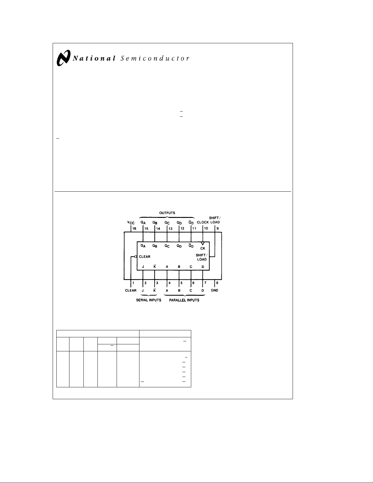
Connection Diagram
towards QD.
A
Dual-In-Line Package
November 1995
trol input is high. Serial data for this mode is entered at the
J-K
inputs. These inputs allow the first stage to perform as a
J-K
or TOGGLE flip flop as shown in the truth table.
The 54HC/74HC logic family is functionally as well as pinout compatible with the standard 54LS/74LS logic family.
All inputs are protected from damage due to static discharge by internal diode clamps to V
and ground.
CC
Features
Y
Typical operating frequency: 45 MHz
Y
Typical propagation delay: 16 ns (clock to Q)
Y
Wide operating supply voltage range: 2 –6V
Y
Low input current: 1 mA maximum
Y
Low quiescent current: 80 mA maximum (74HC Series)
Y
Fanout of 10 LS-TTL loads
MM54HC195/MM74HC195 4-Bit Parallel Shift Register
Top View
TL/F/5324– 1
Order Number MM54HC195 or MM74HC195
Function Table
Inputs Outputs
Clear Shift/ Clock
Load J K ABCD
LXXXXXXXXLLLLH
HL
HH LXXXXXXQA0QB0QC0QD0Q
HH
HH
HH
HH
C
1995 National Semiconductor Corporation RRD-B30M115/Printed in U. S. A.
Serial Parallel
XXabcda b c d d
u
LHXXXXQA0QA0QBnQCnQ
u
LLXXXXLQAnQBnQCnQ
u
HHXXXXHQAnQBnQCnQ
u
HLXXXXQAnQAnQBnQCnQ
u
TL/F/5324
QAQBQCQDQ
Hehigh level (steady state)
e
low level (steady state)
L
e
irrelevant (any input, including transitions)
X
D
e
transition from low to high level
u
e
the level of steady-state input at inputs A, B, C,
a, b, c, d
or D, respectively.
Q
A0,QB0,QC0,QD0
respectively, before the indicated steady-state input condi-
D0
tions were established.
Cn
Q
An,QBn,QCn
Cn
before the most-recent transition of the clock.
Cn
Cn
e
the level of QA,QB,QC,orQD,
e
the level of QA,QB,QC, respectively,
Page 2
Absolute Maximum Ratings (Notes1&2)
Operating Conditions
If Military/Aerospace specified devices are required,
please contact the National Semiconductor Sales
Office/Distributors for availability and specifications.
Supply Voltage (V
CC
)
DC Input Voltage (VIN)
DC Output Voltage (V
OUT
)
Clamp Diode Current (IIK,IOK)
DC Output Current, per pin (I
OUT
)
DC VCCor GND Current, per pin (ICC)
Storage Temperature Range (T
STG
b
b
)
b
0.5 toa7.0V
1.5 to V
CC
0.5 to V
CC
g
g
b
g
65§Ctoa150§C
a
1.5V
a
0.5V
20 mA
25 mA
50 mA
Supply Voltage (V
)26V
CC
DC Input or Output Voltage 0 V
(V
IN,VOUT
)
Operating Temp. Range (TA)
MM74HC
MM54HC
Input Rise or Fall Times
e
V
2.0V(tr,tf) 1000 ns
CC
e
V
4.5V 500 ns
CC
e
V
6.0V 400 ns
CC
Power Dissipation (PD)
(Note 3) 600 mW
S.O. Package only 500 mW
Lead Temp. (T
) (Soldering 10 seconds) 260§C
L
DC Electrical Characteristics (Note 4)
Symbol Parameter Conditions V
CC
A
e
T
25§C
Typ Guaranteed Limits
V
IH
Minimum High Level 2.0V 1.5 1.5 1.5 V
Input Voltage 4.5V 3.15 3.15 3.15 V
6.0V 4.2 4.2 4.2 V
V
IL
Maximum Low Level 2.0V 0.5 0.5 0.5 V
Input Voltage** 4.5V 1.35 1.35 1.35 V
6.0V 1.8 1.8 1.8 V
V
OH
Minimum High Level V
Output Voltage
e
VIHor V
l
I
IN
OUT
IL
s
20 mA 2.0V 2.0 1.9 1.9 1.9 V
l
4.5V 4.5 4.4 4.4 4.4 V
6.0V 6.0 5.9 5.9 5.9 V
e
V
VIHor V
IN
I
l
OUT
I
l
OUT
l
I
IN
OUT
e
V
OL
Maximum Low Level V
Output Voltage
IL
s
4.0 mA 4.5V 4.2 3.98 3.84 3.7 V
l
s
5.2 mA 6.0V 5.7 5.48 5.34 5.2 V
l
VIHor V
IL
s
20 mA 2.0V 0 0.1 0.1 0.1 V
l
4.5V 0 0.1 0.1 0.1 V
6.0V 0 0.1 0.1 0.1 V
e
V
VIHor V
IN
I
l
OUT
I
l
OUT
I
IN
I
CC
Note 1: Absolute Maximum Ratings are those values beyond which damage to the device may occur.
Note 2: Unless otherwise specified all voltages are referenced to ground.
Note 3: Power Dissipation temperature derating Ð plastic ‘‘N’’ package:
Note 4: For a power supply of 5V
designing with this supply. Worst case V
I
**V
Maximum Input V
Current
Maximum Quiescent V
Supply Current I
, and IOZ) occur for CMOS at the higher voltage and so the 6.0V values should be used.
CC
limits are currently tested at 20% of VCC. The above VILspecification (30% of VCC) will be implemented no later than Q1, CY’89.
IL
e
IN
e
IN
OUT
g
10% the worst case output voltages (VOH, and VOL) occur for HC at 4.5V. Thus the 4.5V values should be used when
and VILoccur at V
IH
IL
s
4.0 mA 4.5V 0.2 0.26 0.33 0.4 V
l
s
5.2 mA 6.0V 0.2 0.26 0.33 0.4 V
l
VCCor GND 6.0V
g
0.1
VCCor GND 6.0V 8.0 80 160 mA
e
0 mA
b
12 mW/§C from 65§Cto85§C; ceramic ‘‘J’’ package:b12 mW/§C from 100§Cto125§C.
e
5.5V and 4.5V respectively. (The VIHvalue at 5.5V is 3.85V.) The worst case leakage current (IIN,
CC
74HC 54HC
eb
T
40 to 85§CT
A
g
1.0
Min Max Units
CC
b
b
40
55
eb
A
55 to 125§C
g
a
85
a
125
§
§
Units
1.0 mA
V
C
C
2
Page 3

AC Electrical Characteristics V
CC
5V, T
e
A
25§C, C
e
L
15 pF, t
e
e
t
6ns
r
f
e
Symbol Parameter Conditions Typ Guaranteed Limit Units
f
MAX
t
PHL,tPLH
t
PHL
t
REM
t
REM
t
S
t
S
t
W
t
H
Maximum Operating Frequency 45 30 MHz
Maximum Propagation Delay, Clock to Q 14 24 ns
Maximum Propagation Delay, Reset to Q 16 25 ns
Minimum Removal Time, Shift/Load to Clock 0 ns
Minimum Removal Time, Reset Inactive to Clock 5 ns
Minimum Setup Time, (A, B, C, D, J, K to Clock) 20 ns
Minimum Setup Time, Shift/Load to Clock 20 ns
Minimum Pulse Width Clock or Reset 16 ns
Minimum Hold Time, any Input except Shift/Load 0 ns
AC Electrical Characteristics C
e
L
50 pF, t
Symbol Parameter Conditions V
f
MAX
t
PHL
t
PHL,tPLH
t
THL,tTLH
t
REM
t
REM
t
S
t
S
t
H
t
W
tr,t
C
PD
C
IN
Note 5: CPDdetermines the no load dynamic power consumption, P
Maximum Operating 2.0V 10 6 5 4 MHz
Frequency 4.5V 45 30 24 20 MHz
Maximum Propagation 2.0V 70 150 189 224 ns
Delay, Reset to Q or Q 4.5V 15 30 38 45 ns
Maximum Propagation 2.0V 70 145 183 216 ns
Delay, Clock to Q or Q
Maximum Output Rise 2.0V 30 75 95 110 ns
and Fall Time 4.5V 8 15 19 22 ns
Minimum Removal Time, 2.0Vb20 0 0 ns
Shift Load to Clock 4.5V
Minimum Removal Time, 2.0V 5 5 5 ns
Reset Inactive to Clock 4.5V 5 5 5 ns
Minimum Setup Time, 2.0V 100 125 150 ns
(A, B, C, D, J, K
Minimum Setup Time, 2.0V 100 125 150 ns
Shift/Load to Clock 4.5V 20 25 30 ns
Minimum Hold Time 2.0Vb10 0 0 0 ns
any Input except Shift/Load 4.5V
Minimum Pulse Width, 2.0V 30 80 100 120 ns
Clock or Reset 4.5V 10 16 20 24 ns
Maximum Input Rise 2.0V 1000 1000 1000 ns
f
and Fall Time 4.5V 500 500 500 ns
Power Dissipation 100 pF
Capacitance (Note 5)
to Clock) 4.5V 20 25 30 ns
Maximum Input Capacitance 5 10 10 10 pF
D
e
e
t
6 ns (unless otherwise specified)
r
f
CC
e
T
25§C
A
74HC 54HC
eb
T
40 to 85§CT
A
A
eb
55 to 125§C
Units
Typ Guaranteed Limits
6.0V 50 35 28 24 MHz
6.0V 12 26 32 38 ns
4.5V 15 29 37 43 ns
6.0V 12 25 31 37 ns
6.0V 7 13 16 19 ns
b
6.0Vb20 0 0 ns
20 0 0 ns
6.0V 5 5 5 ns
6.0V 17 21 25 ns
6.0V 17 21 25 ns
b
20 0 0 ns
b
6.0V
20 0 0 ns
6.0V 9 14 18 20 ns
6.0V 400 400 400 ns
2
e
CPDV
faICCVCC, and the no load dynamic current consumption, I
CC
e
CPDVCCfaICC.
S
3
Page 4

Logic and Timing Diagrams
TL/F/5324– 2
TL/F/5324– 3
4
Page 5

Physical Dimensions inches (millimeters)
Ceramic Dual-In-Line Package (J)
Order Number MM54HC195J or MM74HC195J
NS Package Number J16A
5
Page 6

Physical Dimensions inches (millimeters) (Continued)
Molded Dual-In-Line Package (N)
Order Number MM74HC195N
NS Package N16E
MM54HC195/MM74HC195 4-Bit Parallel Shift Register
LIFE SUPPORT POLICY
NATIONAL’S PRODUCTS ARE NOT AUTHORIZED FOR USE AS CRITICAL COMPONENTS IN LIFE SUPPORT
DEVICES OR SYSTEMS WITHOUT THE EXPRESS WRITTEN APPROVAL OF THE PRESIDENT OF NATIONAL
SEMICONDUCTOR CORPORATION. As used herein:
1. Life support devices or systems are devices or 2. A critical component is any component of a life
systems which, (a) are intended for surgical implant support device or system whose failure to perform can
into the body, or (b) support or sustain life, and whose be reasonably expected to cause the failure of the life
failure to perform, when properly used in accordance support device or system, or to affect its safety or
with instructions for use provided in the labeling, can effectiveness.
be reasonably expected to result in a significant injury
to the user.
National Semiconductor National Semiconductor National Semiconductor National Semiconductor
Corporation Europe Hong Kong Ltd. Japan Ltd.
1111 West Bardin Road Fax: (
Arlington, TX 76017 Email: cnjwge@tevm2.nsc.com Ocean Centre, 5 Canton Rd. Fax: 81-043-299-2408
Tel: 1(800) 272-9959 Deutsch Tel: (
Fax: 1(800) 737-7018 English Tel: (
National does not assume any responsibility for use of any circuitry described, no circuit patent licenses are implied and National reserves the right at any time without notice to change said circuitry and specifications.
Fran3ais Tel: (
Italiano Tel: (
a
49) 0-180-530 85 86 13th Floor, Straight Block, Tel: 81-043-299-2309
a
49) 0-180-530 85 85 Tsimshatsui, Kowloon
a
49) 0-180-532 78 32 Hong Kong
a
49) 0-180-532 93 58 Tel: (852) 2737-1600
a
49) 0-180-534 16 80 Fax: (852) 2736-9960
 Loading...