

Page 1
MM54HC192/MM74HC192
Synchronous Decade Up/Down Counters
MM54HC193/MM74HC193
Synchronous Binary Up/Down Counters
General Description
These high speed synchronous counters utilize advanced
silicon-gate CMOS technology to achieve the high noise immunity and low power consumption of CMOS technology,
along with the speeds of low power Schottky TTL. The
MM54HC192/MM74HC192 is a decade counter, and the
MM54HC193/MM74HC193 is a binary counter. Both counters have two separate clock inputs, an UP COUNT input
and a DOWN COUNT input. All outputs of the flip-flops are
simultaneously triggered on the low to high transition of either clock while the other input is held high. The direction of
counting is determined by which input is clocked.
These counters may be preset by entering the desired data
on the DATA A, DATA B, DATA C, and DATA D inputs.
When the LOAD input is taken low the data is loaded independently of either clock input. This feature allows the counters to be used as divide-by-n counters by modifying the
count length with the preset inputs.
In addition both counters can also be cleared. This is accomplished by inputting a high on the CLEAR input. All 4
internal stages are set to a low level independently of either
COUNT input.
Both a BORROW and CARRY output are provided to enable cascading of both up and down counting functions. The
BORROW output produces a negative going pulse when the
counter underflows and the CARRY outputs a pulse when
the counter overflows. The counters can be cascaded by
connecting the CARRY and BORROW outputs of one device to the COUNT UP and COUNT DOWN inputs, respectively, of the next device.
All inputs are protected from damage due to static discharge by diodes to V
CC
Features
Y
Typical propagation delay,
Count up to Q: 28 ns
Y
Typical operating frequency: 27 MHz
Y
Wide power supply range: 2 –6V
Y
Low quiescent supply current: 80 mA maximum
(74HC Series)
Y
Low input current: 1 mA maximum
Y
4 mA output drive
and ground.
January 1988
MM54HC192/MM74HC192 Synchronous Decade Up/Down Counters
MM54HC193/MM74HC193 Synchronous Binary Up/Down Counters
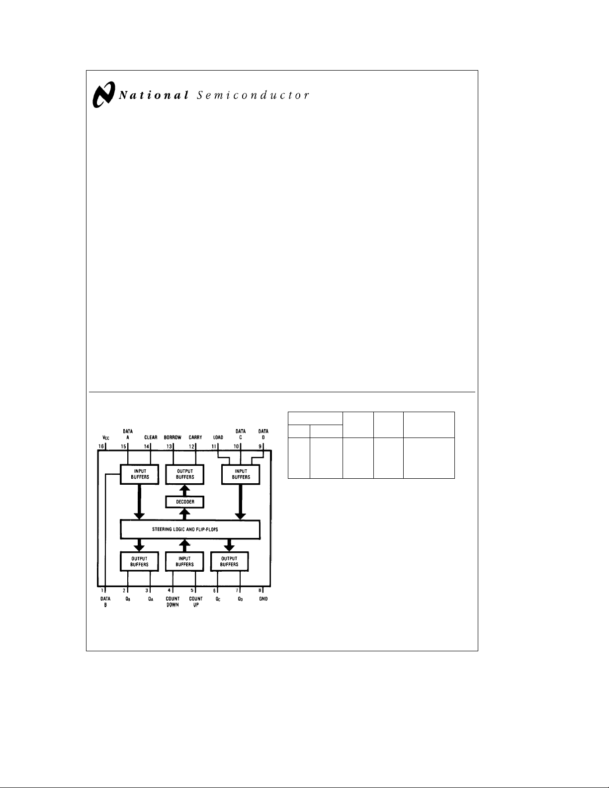
Connection Diagram
Dual-In-Line Package
Order Number MM54HC192/193 or MM74HC192/193
C
1995 National Semiconductor Corporation RRD-B30M115/Printed in U. S. A.
TL/F/5011
TL/F/5011– 1
Truth Table
Count
Up Down
u
H
X X H X Clear
X X L L Load
Hehigh level
e
L
low level
e
transition from low-to-high
u
e
X
don’t care
Clear Load Function
H L H Count Up
u
L H Count Down
Page 2
Absolute Maximum Ratings (Notes1&2)
Operating Conditions
If Military/Aerospace specified devices are required,
please contact the National Semiconductor Sales
Office/Distributors for availability and specifications.
Supply Voltage (V
CC
)
DC Input Voltage (VIN)
DC Output Voltage (V
OUT
)
Clamp Diode Current (IIK,IOK)
DC Output Current, per pin (I
OUT
)
DC VCCor GND Current, per pin (ICC)
Storage Temperature Range (T
STG
b
b
)
b
0.5 toa7.0V
1.5 to V
CC
0.5 to V
CC
g
g
b
g
65§Ctoa150§C
a
1.5V
a
0.5V
20 mA
25 mA
50 mA
Supply Voltage (V
)26V
CC
DC Input or Output Voltage 0 V
(V
IN,VOUT
)
Operating Temp. Range (TA)
MM74HC
MM54HC
Input Rise or Fall Times
e
V
2V(tr,tf) 1000 ns
CC
e
V
4.5V 500 ns
CC
e
V
6.0V 400 ns
CC
Power Dissipation (PD)
(Note 3) 600 mW
S.O. Package only 500 mW
Lead Temp. (T
) (Soldering 10 seconds) 260§C
L
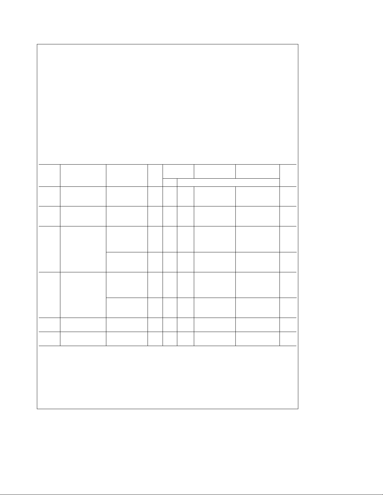
DC Electrical Characteristics (Note 4)
Symbol Parameter Conditions V
CC
A
e
T
25§C
Typ Guaranteed Limits
V
IH
Minimum High Level 2.0V 1.5 1.5 1.5 V
Input Voltage 4.5V 3.15 3.15 3.15 V
6.0V 4.2 4.2 4.2 V
V
IL
Maximum Low Level 2.0V 0.5 0.5 0.5 V
Input Voltage** 4.5V 1.35 1.35 1.35 V
6.0V 1.8 1.8 1.8 V
V
OH
Minimum High Level V
Output Voltage
e
VIHor V
l
I
IN
OUT
IL
s
20 mA 2.0V 2.0 1.9 1.9 1.9 V
l
4.5V 4.5 4.4 4.4 4.4 V
6.0V 6.0 5.9 5.9 5.9 V
e
V
VIHor V
IN
I
l
OUT
I
l
OUT
l
I
IN
OUT
e
V
OL
Maximum Low Level V
Output Voltage
IL
s
4.0 mA 4.5V 4.2 3.98 3.84 3.7 V
l
s
5.2 mA 6.0V 5.7 5.48 5.34 5.2 V
l
VIHor V
IL
s
20 mA 2.0V 0 0.1 0.1 0.1 V
l
4.5V 0 0.1 0.1 0.1 V
6.0V 0 0.1 0.1 0.1 V
e
V
VIHor V
IN
I
l
OUT
I
l
OUT
I
IN
I
CC
Note 1: Absolute Maximum Ratings are those values beyond which damage to the device may occur.
Note 2: Unless otherwise specified all voltages are referenced to ground.
Note 3: Power Dissipation temperature derating Ð plastic ‘‘N’’ package:
Note 4: For a power supply of 5V
with this supply. Worst case V
I
**V
Maximum Input V
Current
Maximum Quiescent V
Supply Current I
g
and VILoccur at V
) occur for CMOS at the higher voltage and so the 6.0V values should be used.
OZ
limits are currently tested at 20% of VCC. The above VILspecification (30% of VCC) will be implemented no later than Q1, CY’89.
IL
IH
e
IN
e
IN
OUT
10% the worst case output voltages (VOH, and VOL) occur for HC at 4.5V. Thus the 4.5V values should be used when designing
IL
s
4.0 mA 4.5V 0.2 0.26 0.33 0.4 V
l
s
5.2 mA 6.0V 0.2 0.26 0.33 0.4 V
l
VCCor GND 6.0V
g
0.1
VCCor GND 6.0V 8.0 80 160 mA
e
0 mA
b
12 mW/§C from 65§Cto85§C; ceramic ‘‘J’’ package:b12 mW/§C from 100§Cto125§C.
e
5.5V and 4.5V respectively. (The VIHvalue at 5.5V is 3.85V.) The worst case leakage current (IIN,ICC, and
CC
74HC 54HC
eb
T
40 to 85§CT
A
g
1.0
Min Max Units
V
§
§
Units
b
b
40
55
eb
A
55 to 125§C
g
CC
a
85
a
125
1.0 mA
C
C
2
Page 3
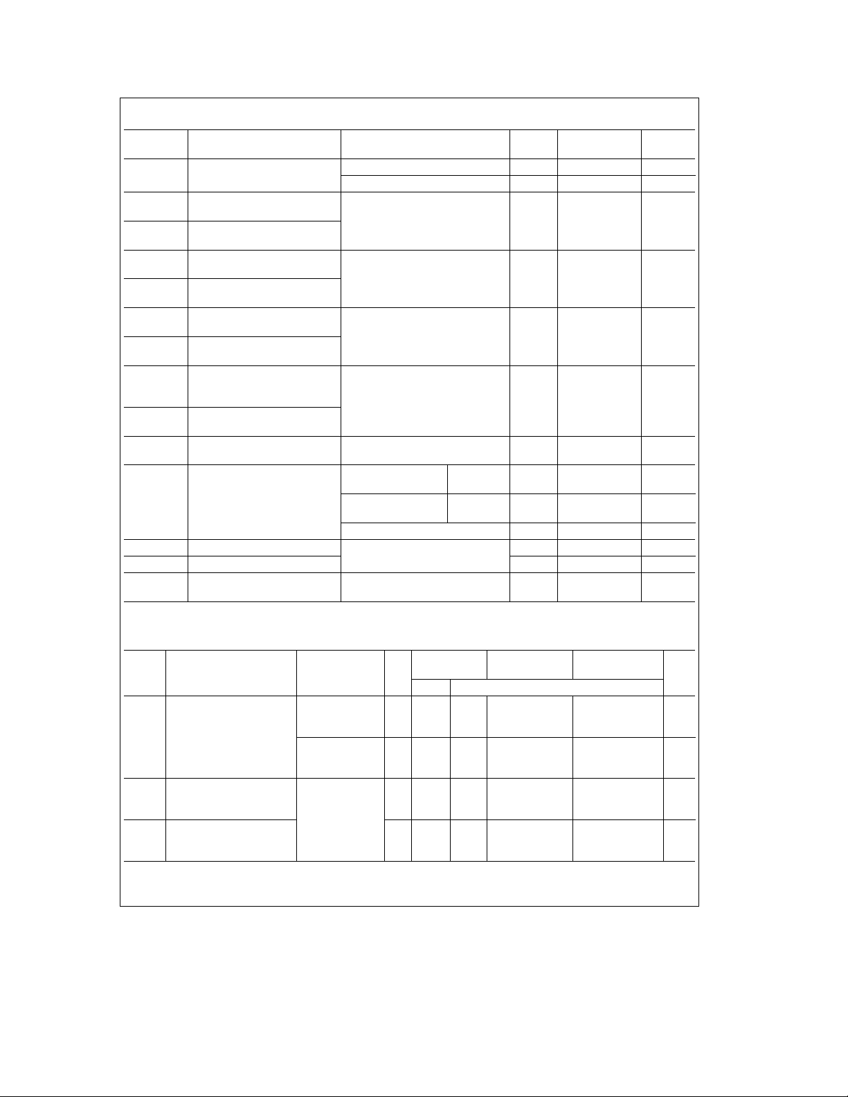
AC Electrical Characteristics T
e
A
25§C, V
CC
e
5.0V, t
e
e
t
r
f
6 ns, C
e
15 pF (unless otherwise specified)
L
Symbol Parameter Conditions Typ
f
MAX
t
PLH
t
PHL
t
PLH
t
PHL
t
PLH
t
PHL
t
PLH
t
PHL
t
PHL
t
W
Maximum Clock Frequency
Maximum Propagation Delay 17 26 ns
Low to High
Maximum Propagation Delay 18 24 ns
High to Low
Maximum Propagation Delay 16 24 ns
Low to High Count Down to
Maximum Propagation Delay
High to Low
Maximum Propagation Delay 28 40 ns
Low to High
Maximum Propagation Delay
High to Low
Maximum Propagation Delay 30 42 ns
Low to High
Maximum Propagation Delay 40 55 ns
High to Low
Maximum Propagation Delay
High to Low
Minimum Pulse Width
Count Up 27 20 MHz
Count Down 31 24 MHz
Count Up to Carry
Borrow
Count Up Or
Down to Q
15 24 ns
36 52 ns
Data or
Load to Q
Clear to Q
Clear
Load
’HC192 40 52 ns
’HC193 20 26 ns
’HC192 40 52 ns
’HC193 10 20 ns
35 47 ns
Count Up/Down 15 22 ns
t
SD
t
HD
t
REM
Minimum Setup time
Minimum Hold Time
Minimum Removal Time
Data to Load
Clear Inactive
to Clock
10 20 ns
b
Guaranteed
Limit
Units
30 ns
10 ns
AC Electrical Characteristics V
CC
e
2.0V to 6.0V, C
Symbol Parameter Conditions V
Count Up 4.5V 25 18 14 12 MHz
f
Maximum Clock Frequency
MAX
Count Down 4.5V 27 20 16 11 MHz
t
Maximum Propagation Delay 2.0V 30 140 175 210 ns
PLH
Low to High 4.5V 13 28 35 42 ns
Count Up
t
Maximum Propagation Delay
PHL
High to Low 4.5V 16 26 33 39 ns
to Carry
CC
e
L
e
T
25§C
A
50 pF, t
e
e
t
6ns
r
f
74HC 54HC
eb
T
40 to 85§CT
A
A
eb
55 to 125§C
Units
Typ Guaranteed Limits
2.0V 5 3 2.5 2 MHz
6.0V 29 20 16 13 MHz
2.0V 5 4 3 2 MHz
6.0V 31 23 18 12 MHz
6.0V 11 24 30 36 ns
2.0V 39 130 163 195 ns
6.0V 14 22 28 33 ns
3
Page 4

AC Electrical Characteristics (Continued) V
CC
Symbol Parameter Conditions V
t
t
t
t
t
t
t
Maximum Propagation Delay Count Down 2.0V 39 130 163 195 ns
PLH,tPHL
Maximum Output Rise 2.0V 30 75 95 110 ns
TLH,tTHL
and Fall Time 4.5V 8 15 19 22 ns
Maximum Propagation Delay 2.0V 77 215 269 323 ns
PLH
Low to High 4.5V 35 43 54 65 ns
Maximum Propagation Delay
PHL
High to Low 4.5V 45 55 69 83 ns
Maximum Propagation Delay 2.0V 85 230 288 345 ns
PLH
Low to High 4.5V 37 46 58 69 ns
Maximum Propagation Delay
PHL
High to Low 4.5V 47 58 73 87 ns
Maximum Propagation Delay 2.0V 85 265 331 398 ns
PHL
High to Low Clear to Q 4.5V 42 53 66 80 ns
to Borrow 4.5V 16 26 33 39 ns
Count Up Or 6.0V 30 37 46 55 ns
Down to Q
Data or 6.0V 30 39 49 59 ns
Load to Q
Clear 2.0V 119 260 325 390 ns
or ’HC192 4.5V 42 52 65 78 ns
Load 6.0V 38 45 56 68 ns
Load ’HC193 4.5V 10 20 25 30 ns
t
W
Minimum Pulse Width
Count Up/Down 4.5V 17 22 28 33 ns
Clear ’HC193 4.5V 21 26 33 39 ns
t
t
t
t
C
C
Minimum Setup Time
SD
Minimum Hold Time 4.5Vb30 0 0 ns
HD
Minimum Removal Time Clear Inactive 2.0Vb20 10 10 10 ns
REM
Maximum Count Up or Down
r,tf
Input Rise & Fall Time
Input Capacitance 5 10 10 10 pF
IN
Power Dissipation Capacitance (Note 5) 100 pF
PD
Note 5: CPDdetermines the no load dynamic power consumption, P
Data
To
Load
to Clock 4.5V
e
CPDV
D
CC
e
2.0V to 6.0V, C
T
A
CC
e
25§C
e
L
T
e
50 pF, t
r
74HC 54HC
eb
40 to 85§CT
A
e
t
6ns
f
eb
A
55 to 125§C
Units
Typ Guaranteed Limits
6.0V 14 22 28 33 ns
6.0V 7 13 16 19 ns
2.0V 95 275 344 413 ns
6.0V 38 47 59 71 ns
2.0V 102 290 363 435 ns
6.0V 39 49 61 74 ns
6.0V 38 45 56 68 ns
2.0V 31 100 125 150 ns
6.0V 9 17 21 26 ns
2.0V 43 110 138 165 ns
6.0V 15 19 24 29 ns
2.0V 70 130 163 195 ns
6.0V 19 22 28 33 ns
2.0V 30 100 125 150 ns
4.5V 10 20 25 30 ns
6.0V 9 17 22 25 ns
b
2.0V
30 0 0 0 ns
6.0Vb30 0 0 ns
b
310 10 10 ns
b
210 10 10 ns
6.0V
2.0V 500 500 500 ns
4.5V 300 300 300 ns
6.0V 200 200 200 ns
2
faICCVCC, and the no load dynamic current consumption, I
e
CPDVCCfaICC.
S
4
Page 5

Logic Diagrams
TL/F/5011– 2
MM54HC192 Synchronous 4-Bit Up/Down Decade Counter
5
Page 6

Logic Diagrams (Continued)
TL/F/5011– 3
MM54HC193 Synchronous 4-Bit Up/Down Binary Counter
6
Page 7

Logic Waveforms
’HC192 Synchronous Decade Counters
Typical Clear, Load, and Count Sequences
Sequences:
(1) Clear outputs to zero
(2) Load (preset) to BCD seven.
(3) Count up to eight, nine, carry, zero, one and two.
(4) Count down to one, zero, borrow, nine, eight, and seven.
’HC193 Synchronous Binary Counters
Typical Clear, Load, and Count Sequences
Sequence:
(1) Clear outputs to zero.
(2) Load (preset) to binary thirteen
(3) Count up to fourteen, fifteen, carry, zero, one, and two.
(4) Count down to one, zero, borrow, fifteen, fourteen, and thirteen.
Note A: Clear overrides load data, and count inputs.
Note B: When counting up, count-down input must be high; when counting down, count-up input must be high.
TL/F/5011– 4
TL/F/5011– 5
7
Page 8

Physical Dimensions inches (millimeters)
Order Number MM54HC192J, MM54HC193J, MM74HC192J or MM74HC193J
NS Package J16A
Order Number MM74HC192N or MM74HC193N
NS Package N16E
MM54HC193/MM74HC193 Synchronous Binary Up/Down Counters
MM54HC192/MM74HC192 Synchronous Decade Up/Down Counters
LIFE SUPPORT POLICY
NATIONAL’S PRODUCTS ARE NOT AUTHORIZED FOR USE AS CRITICAL COMPONENTS IN LIFE SUPPORT
DEVICES OR SYSTEMS WITHOUT THE EXPRESS WRITTEN APPROVAL OF THE PRESIDENT OF NATIONAL
SEMICONDUCTOR CORPORATION. As used herein:
1. Life support devices or systems are devices or 2. A critical component is any component of a life
systems which, (a) are intended for surgical implant support device or system whose failure to perform can
into the body, or (b) support or sustain life, and whose be reasonably expected to cause the failure of the life
failure to perform, when properly used in accordance support device or system, or to affect its safety or
with instructions for use provided in the labeling, can effectiveness.
be reasonably expected to result in a significant injury
to the user.
National Semiconductor National Semiconductor National Semiconductor National Semiconductor
Corporation Europe Hong Kong Ltd. Japan Ltd.
1111 West Bardin Road Fax: (
Arlington, TX 76017 Email: cnjwge@tevm2.nsc.com Ocean Centre, 5 Canton Rd. Fax: 81-043-299-2408
Tel: 1(800) 272-9959 Deutsch Tel: (
Fax: 1(800) 737-7018 English Tel: (
National does not assume any responsibility for use of any circuitry described, no circuit patent licenses are implied and National reserves the right at any time without notice to change said circuitry and specifications.
Fran3ais Tel: (
Italiano Tel: (
a
49) 0-180-530 85 86 13th Floor, Straight Block, Tel: 81-043-299-2309
a
49) 0-180-530 85 85 Tsimshatsui, Kowloon
a
49) 0-180-532 78 32 Hong Kong
a
49) 0-180-532 93 58 Tel: (852) 2737-1600
a
49) 0-180-534 16 80 Fax: (852) 2736-9960
 Loading...