

Page 1
MM74HC160 Synchronous
Decade Counter with Asynchronous Clear
MM54HC161/MM74HC161 Synchronous
Binary Counter with Asynchronous Clear
MM54HC162/MM74HC162 Synchronous
Decade Counter with Synchronous Clear
MM54HC163/MM74HC163 Synchronous
Binary Counter with Synchronous Clear
General Description
The MM54HC160/MM74HC160, MM54HC161/
MM74HC161, MM54HC162/MM74HC162, and
MM54HC163/MM74HC163 synchronous presettable counters utilize advanced silicon-gate CMOS technology and internal look-ahead carry logic for use in high speed counting
applications. They offer the high noise immunity and low
power consumption inherent to CMOS with speeds similar
to low power Schottky TTL. The ’HC160 and the ’HC162 are
4 bit decade counters, and the ’HC161 and the ’HC163 are
4 bit binary counters. All flip-flops are clocked simultaneously on the low to high transition (positive edge) of the CLOCK
input waveform.
These counters may be preset using the LOAD input. Presetting of all four flip-flops is synchronous to the rising edge
of CLOCK. When LOAD is held low counting is disabled and
the data on the A, B, C, and D inputs is loaded into the
counter on the rising edge of CLOCK. If the load input is
taken high before the positive edge of CLOCK the count
operation will be unaffected.
All of these counters may be cleared by utilizing the CLEAR
input. The clear function on the MM54HC162/MM74HC162
and MM54HC163/MM74HC163 counters are synchronous
to the clock. That is, the counters are cleared on the positive edge of CLOCK while the clear input is held low.
The MM54HC160/MM74HC160 and MM54HC161/
MM74HC161 counters are cleared asynchronously. When
the CLEAR is taken low the counter is cleared immediately
regardless of the CLOCK.
Two active high enable inputs (ENP and ENT) and a RIPPLE CARRY (RC) output are provided to enable easy cascading of counters. Both ENABLE inputs must be high to
count. The ENT input also enables the RC output. When
enabled, the RC outputs a positive pulse when the counter
overflows. This pulse is approximately equal in duration to
the high level portion of the Q
to successive cascaded stages to facilitate easy implementation of N-bit counters.
All inputs are protected from damage due to static discharge by diodes to V
CC
Features
Y
Typical operating frequency: 40 MHz
Y
Typical propagation delay; clock to Q: 18 ns
Y
Low quiescent current: 80 mA maximum (74HC Series)
Y
Low input current: 1 mA maximum
Y
Wide power supply range: 2–6V
output. The RC output is fed
A
and ground.
74HC160/MM54/74HC161/MM54/74HC162/MM54/74HC163
January 1992
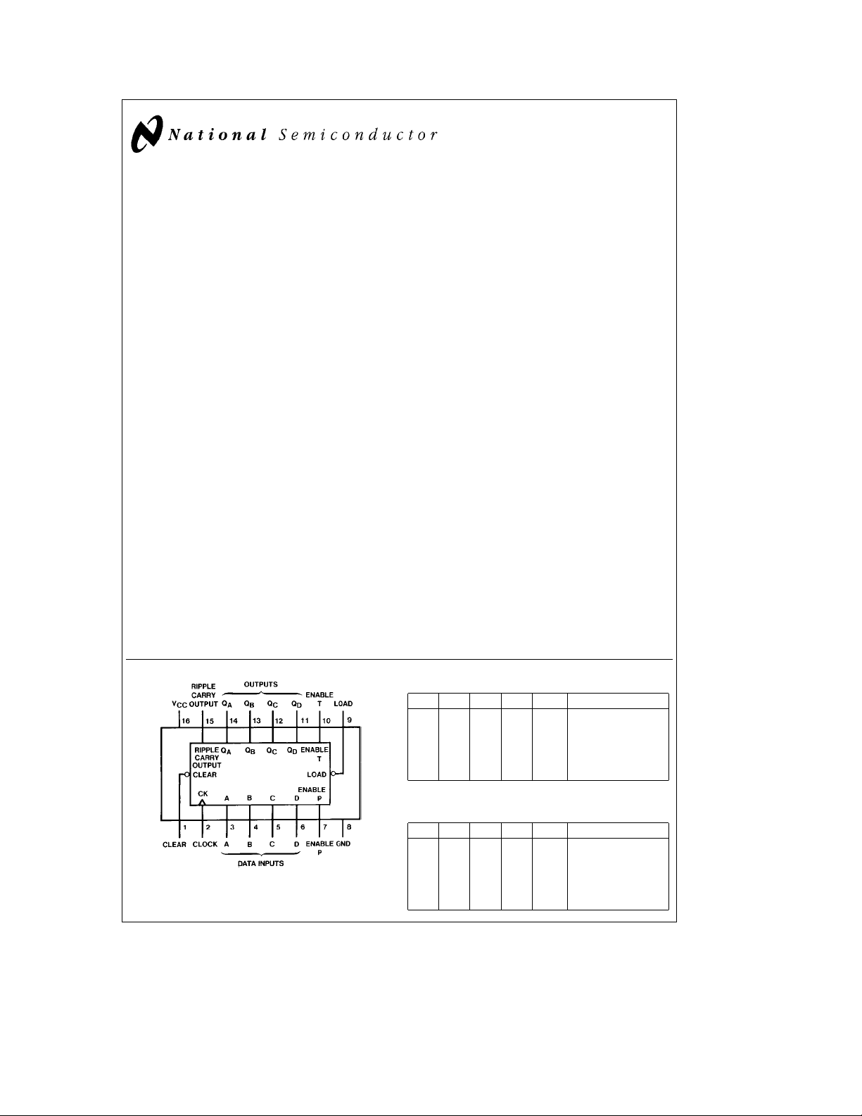
Connection Diagram
Order Number MM54HC161/162/163
or MM74HC160/161/162/163
C
1995 National Semiconductor Corporation RRD-B30M115/Printed in U. S. A.
TL/F/5008
TL/F/5008– 1
Truth Tables
’HC160/HC161
CLK CLR ENP ENT Load Function
X L X X X Clear
X H H L H Count & RC disabled
X H L H H Count disabled
X H L L H Count & RC disabled
H X X L Load
u
H H H H Increment Counter
u
Hehigh level, Lelow level
e
don’t care,
X
CLK CLR ENP ENT Load Function
u
X H H L H Count & RC disabled
X H L H H Count disabled
X H L L H Count & RC disabled
u
u
e
low to high transition
u
’HC162/HC163
L X X X Clear
H X X L Load
H H H H Increment Counter
Page 2
Absolute Maximum Ratings (Notes1&2)
Operating Conditions
If Military/Aerospace specified devices are required,
please contact the National Semiconductor Sales
Office/Distributors for availability and specifications.
Supply Voltage (V
CC
)
DC Input Voltage (VIN)
DC Output Voltage (V
OUT
)
Clamp Diode Current (IIK,IOK)
DC Output Current, per pin (I
OUT
)
DC VCCor GND Current, per pin (ICC)
Storage Temperature Range (T
STG
b
b
)
b
0.5 toa7.0V
1.5 to V
CC
0.5 to V
CC
g
g
b
g
65§Ctoa150§C
a
1.5V
a
0.5V
20 mA
25 mA
50 mA
Power Dissipation (PD)
Supply Voltage (V
DC Input or Output Voltage 0 V
(V
IN,VOUT
Operating Temp. Range (T
MM74HC
MM54HC
Input Rise or Fall Times
)26V
CC
)
e
V
2.0V(tr,tf) 1000 ns
CC
e
4.5V 500 ns
V
CC
e
6.0V 400 ns
V
CC
(Note 3) 600 mW
S.O. Package only 500 mW
Lead Temp. (T
) (Soldering 10 seconds) 260§C
L
DC Electrical Characteristics (Note 4)
Symbol Parameter Conditions V
CC
A
e
T
25§C
Typ Guaranteed Limits
V
IH
Minimum High Level 2.0V 1.5 1.5 1.5 V
Input Voltage 4.5V 3.15 3.15 3.15 V
6.0V 4.2 4.2 4.2 V
V
IL
Maximum Low Level 2.0V 0.5 0.5 0.5 V
Input Voltage** 4.5V 1.35 1.35 1.35 V
6.0V 1.8 1.8 1.8 V
V
OH
Minimum High Level V
Output Voltage
e
VIHor V
l
I
IN
OUT
IL
s
20 mA 2.0V 2.0 1.9 1.9 1.9 V
l
4.5V 4.5 4.4 4.4 4.4 V
6.0V 6.0 5.9 5.9 5.9 V
e
V
VIHor V
IN
I
l
OUT
I
l
OUT
l
I
IN
OUT
e
V
OL
Maximum Low Level V
Output Voltage
IL
s
4.0 mA 4.5V 4.2 3.98 3.84 3.7 V
l
s
5.2 mA 6.0V 5.7 5.48 5.34 5.2 V
l
VIHor V
IL
s
20 mA 2.0V 0 0.1 0.1 0.1 V
l
4.5V 0 0.1 0.1 0.1 V
6.0V 0 0.1 0.1 0.1 V
e
V
VIHor V
IN
I
l
OUT
I
l
OUT
I
IN
I
CC
Note 1: Absolute Maximum Ratings are those values beyond which damage to the device may occur.
Note 2: Unless otherwise specified all voltages are referenced to ground.
Note 3: Power Dissipation temperature derating Ð plastic ‘‘N’’ package:
Note 4: For a power supply of 5V
with this supply. Worst case V
I
**V
Maximum Input V
Current
Maximum Quiescent V
Supply Current I
g
and VILoccur at V
) occur for CMOS at the higher voltage and so the 6.0V values should be used.
OZ
limits are currently tested at 20% of VCC. The above VILspecification (30% of VCC) will be implemented no later than Q1, CY’89.
IL
IH
e
IN
e
IN
OUT
10% the worst case output voltages (VOH, and VOL) occur for HC at 4.5V. Thus the 4.5V values should be used when designing
IL
s
4.0 mA 4.5V 0.2 0.26 0.33 0.4 V
l
s
5.2 mA 6.0V 0.2 0.26 0.33 0.4 V
l
VCCor GND 6.0V
g
0.1
VCCor GND 6.0V 8.0 80 160 mA
e
0 mA
b
12 mW/§C from 65§Cto85§C; ceramic ‘‘J’’ package:b12 mW/§C from 100§Cto125§C.
e
5.5V and 4.5V respectively. (The VIHvalue at 5.5V is 3.85V.) The worst case leakage current (IIN,ICC, and
CC
74HC 54HC
eb
T
40 to 85§CT
A
g
1.0
Min Max Units
)
A
b
b
40
55
eb
A
55 to 125§C
g
a
a
1.0 mA
CC
85
125
V
C
§
C
§
Units
2
Page 3

AC Electrical Characteristics V
CC
5V, T
e
A
25§C, C
e
L
15 pF, t
e
e
t
6ns
r
f
e
Symbol Parameter Conditions Typ Guaranteed Limit Units
f
MAX
t
PHL,tPLH
t
PHL,tPLH
t
PHL,tPLH
t
PHL
t
REM
t
S
t
H
t
W
Maximum Operating Frequency 43 30 MHz
Maximum Propagation Delay, Clock to RC 30 35 ns
Maximum Propagation Delay, Clock to Q 29 34 ns
Maximum Propagation Delay, ENT to RC 18 32 ns
Maximum Propagation Delay, Clear to Q or RC 27 38 ns
Minimum Removal Time, Clear to Clock 10 20 ns
Minimum Set Up Time Clear, Load, 30 ns
Enable or Data to Clock
Minimum Hold Time, Data from Clock 5 ns
Minimum Pulse Width Clock, 16 ns
Clear, or Load
AC Electrical Characteristics C
e
L
Symbol Parameter Conditions V
f
MAX
t
PHL
t
PLH
t
PHL
t
PLH
t
PHL
t
PLH
t
PHL
t
PHL
t
REM
t
S
t
S
t
S
t
H
Maximum Operating 2.0V 10 5 4 4 MHz
Frequency 4.5V 40 27 21 18 MHz
Maximum Propagation 2.0V 100 215 271 320 ns
Delay, Clock to RC 4.5V 32 43 54 64 ns
Maximum Propagation 2.0V 88 175 220 260 ns
Delay, Clock to RC 4.5V 18 35 44 52 ns
Maximum Propagation 2.0V 95 205 258 305 ns
Delay, Clock to Q 4.5V 30 41 52 61 ns
Maximum Propagation 2.0V 85 170 214 253 ns
Delay, Clock to Q 4.5V 17 34 43 51 ns
Maximum Propagation 2.0V 90 195 246 291 ns
Delay, ENT to RC 4.5V 28 39 49 58 ns
Maximum Propagation 2.0V 80 160 202 238 ns
Delay, ENT to RC 4.5V 16 32 40 48 ns
Maximum Propagation 2.0V 100 220 275 325 ns
Delay, Clear to RC 4.5V 32 44 55 66 ns
Maximum Propagation 2.0V 100 210 260 315 ns
Delay, Clear to Q 4.5V 32 42 52 63 ns
Minimum Removal Time 2.0V 125 158 186 ns
Clear to Clock 4.5V 25 32 37 ns
Minimum Setup 2.0V 150 190 225 ns
Time Clear or Data 4.5V 30 38 45 ns
to Clock 6.0V 26 32 38 ns
Minimum Setup 2.0V 135 170 200 ns
Time Load 4.5V 27 34 41 ns
to Clock 6.0V 23 29 35 ns
Minimum Setup 2.0V 175 220 260 ns
Time Enable 4.5V 35 44 52 ns
to Clock 6.0V 30 37 44 ns
Minimum Hold Time 2.0V 50 63 75 ns
Data from Clock 4.5V 10 13 15 ns
e
50 pF, t
CC
e
t
6 ns (unless otherwise specified)
r
f
e
T
25§C
A
74HC 54HC
eb
T
A
40 to 85§CT
A
eb
55 to 125§C
Units
Typ Guaranteed Limits
6.0V 45 32 25 21 MHz
6.0V 28 37 46 54 ns
6.0V 15 30 37 44 ns
6.0V 26 35 44 52 ns
6.0V 14 29 36 43 ns
6.0V 24 33 42 49 ns
6.0V 14 27 34 41 ns
6.0V 28 37 47 55 ns
6.0V 28 36 45 54 ns
6.0V 21 27 32 ns
6.0V 9 11 13 ns
3
Page 4

AC Electrical Characteristics (Continued) C
Symbol Parameter Conditions V
t
H
t
W
t
TLH,tTHL
tr,t
C
PD
C
IN
Note 5: CPDdetermines the no load dynamic power consumption, P
e
I
S
Minimum Hold Time 2.0V 0 0 0 ns
Enable, Load or Clear 4.5V 0 0 0 ns
to Clock 6.0V 0 0 0 ns
Minimum Pulse Width 2.0V 80 100 120 ns
Clock, Clear, or 4.5V 16 20 24 ns
Load 6.0V 14 17 20 ns
Maximum 2.0V 40 75 95 110 ns
Output Rise and 4.5V 8 15 19 22 ns
Fall Time 6.0V 7 13 16 19 ns
Maximum Input Rise and 2.0V 1000 1000 1000 ns
f
Fall Time 4.5V 500 500 500 ns
Power Dissipation (per package) 90 pF
Capacitance (Note 5)
Maximum Input Capacitance 5 10 10 10 pF
CPDVCCfaICC.
CC
6.0V 400 400 400 ns
D
Logic Diagrams
MM54HC160/MM74HC160 or MM54HC162/MM74HC162
e
L
T
50 pF, t
e
25§C
A
e
e
t
6 ns (unless otherwise specified)
r
f
74HC 54HC
eb
T
40 to 85§CT
A
Typ Guaranteed Limits
2
e
CPDV
faICCVCC, and the no load dynamic current consumption,
CC
A
eb
55 to 125§C
Units
MM54HC161/MM74HC161 or MM54HC163/MM74HC163
4
TL/F/5008– 2
TL/F/5008– 3
Page 5

Logic Waveforms
160, 162 Synchronous Decade Counters Typical Clear, Preset, Count and Inhibit Sequences
Sequence: TL/F/5008– 4
(1) Clear outputs to zero
(2) Preset to BCD seven
(3) Count to eight, nine, zero, one, two, and three
(4) Inhibit
161, 163 Synchronous Binary Counters Typical Clear, Preset, Count and Inhibit Sequences
Sequence: TL/F/5008– 5
(1) Clear outputs to zero
(2) Preset to binary twelve
(3) Count to thirteen, fourteen, fifteen, zero, one and two
(4) Inhibit
5
Page 6

Physical Dimensions inches (millimeters)
Order Number MM54HC160J, MM54HC161J, MM54HC162J, MM54HC163J,
MM74HC160J, MM74HC161J, MM74HC162J, MM74HC163J
NS Package J16A
74HC160/MM54/74HC161/MM54/74HC162/MM54/74HC163
Order Number MM74HC160N, MM74HC161N, MM74HC162N, MM74HC163N
LIFE SUPPORT POLICY
NATIONAL’S PRODUCTS ARE NOT AUTHORIZED FOR USE AS CRITICAL COMPONENTS IN LIFE SUPPORT
DEVICES OR SYSTEMS WITHOUT THE EXPRESS WRITTEN APPROVAL OF THE PRESIDENT OF NATIONAL
SEMICONDUCTOR CORPORATION. As used herein:
1. Life support devices or systems are devices or 2. A critical component is any component of a life
systems which, (a) are intended for surgical implant support device or system whose failure to perform can
into the body, or (b) support or sustain life, and whose be reasonably expected to cause the failure of the life
failure to perform, when properly used in accordance support device or system, or to affect its safety or
with instructions for use provided in the labeling, can effectiveness.
be reasonably expected to result in a significant injury
to the user.
National Semiconductor National Semiconductor National Semiconductor National Semiconductor
Corporation Europe Hong Kong Ltd. Japan Ltd.
1111 West Bardin Road Fax: (
Arlington, TX 76017 Email: cnjwge@tevm2.nsc.com Ocean Centre, 5 Canton Rd. Fax: 81-043-299-2408
Tel: 1(800) 272-9959 Deutsch Tel: (
Fax: 1(800) 737-7018 English Tel: (
National does not assume any responsibility for use of any circuitry described, no circuit patent licenses are implied and National reserves the right at any time without notice to change said circuitry and specifications.
Fran3ais Tel: (
Italiano Tel: (
NS Package N16E
a
49) 0-180-530 85 86 13th Floor, Straight Block, Tel: 81-043-299-2309
a
49) 0-180-530 85 85 Tsimshatsui, Kowloon
a
49) 0-180-532 78 32 Hong Kong
a
49) 0-180-532 93 58 Tel: (852) 2737-1600
a
49) 0-180-534 16 80 Fax: (852) 2736-9960
 Loading...