

查询CD4023BC供应商
CD4023BM/CD4023BC
Buffered Triple 3-Input NAND Gate
CD4025BM/CD4025BC
Buffered Triple 3-Input NOR Gate
February 1988
CD4023BM/CD4023BC Buffered Triple 3-Input NAND Gate
CD4025BM/CD4025BC Buffered Triple 3-Input NOR Gate
General Description
These triple gates are monolithic complementary MOS
(CMOS) integrated circuits constructed with N- and P-channel enhancement mode transistors. They have equal source
and sink current capabilities and conform to standard B series output drive. The devices also have buffered outputs
which improve transfer characteristics by providing very
high gain. All inputs are protected against static discharge
with diodes to V
DD
and VSS.
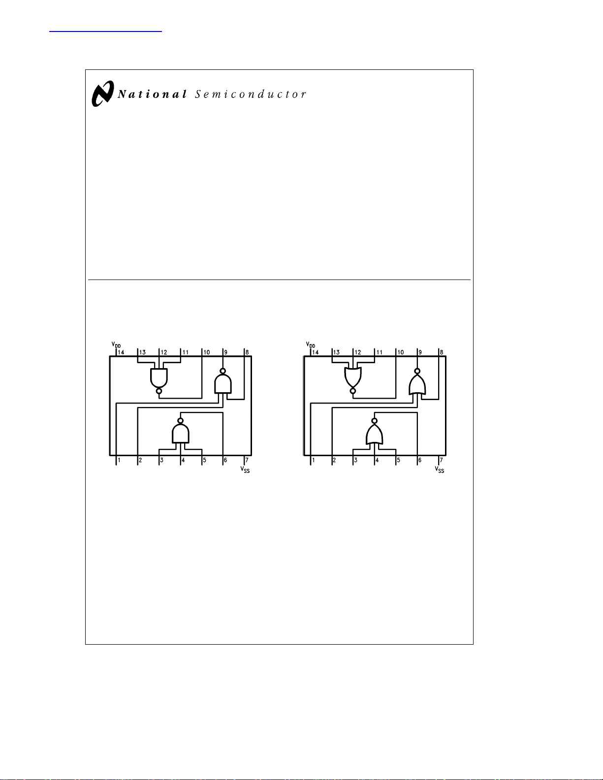
Connection Diagrams
CD4023BM/CD4023BC
Dual-In-Line Package
Top View
TL/F/5956– 1
Features
Y
Wide supply voltage range 3.0V to 15V
Y
High noise immunity 0.45 VDD(typ.)
Y
Low power TTL fan out of 2 driving 74L
compatibility or 1 driving 74LS
Y
5V–10V–15V parametric ratings
Y
Symmetrical output characteristics
Y
Maximum input leakage 1 mA at 15V over full
temperature range
CD4025BM/CD4025BC
Dual-In-Line Package
Top View
TL/F/5956– 2
Order Number CD4023B or CD4025B
C
1995 National Semiconductor Corporation RRD-B30M105/Printed in U. S. A.
TL/F/5956
Absolute Maximum Ratings (Notes1&2)
If Military/Aerospace specified devices are required,
please contact the National Semiconductor Sales
Office/Distributors for availability and specifications.
DC Supply Voltage (V
DD
)
Input Voltage (VIN)
Storage Temp. Range (TS)
b
0.5 VDCtoa18 V
b
0.5 VDCto V
a
0.5 V
DD
b
65§Ctoa150§C
DC
DC
Recommended Operating
Conditions
DC Supply Voltage (VDD)5V
Input Voltage (VIN)0V
Operating Temperature Range (TA)
CD4023BM, CD4025BM
CD4023BC, CD4025BC
Power Dissipation (PD)
Dual-In-Line 700 mW
Small Outline 500 mW
Lead Temperature (T
(Soldering, 10 seconds) 260
)
L
C
§
DC Electrical Characteristics CD4023BM, CD4025BM (Note 2)
Symbol Parameter Conditions
I
Quiescent Device Current V
DD
V
Low Level Output Voltage V
OL
V
High Level Output Voltage V
OH
V
Low Level Input Voltage V
IL
V
High Level Input Voltage V
IH
I
Low Level Output Current V
OL
(Note 3) V
I
High Level Output Current V
OH
(Note 3) V
I
Input Current V
IN
e
5V 0.25 0.004 0.25 7.5 mA
DD
e
10V 0.5 0.005 0.5 15 mA
V
DD
e
15V 1.0 0.006 1.0 30 mA
V
DD
e
5V 0.05 0 0.05 0.05 V
DD
e
10V 0.05 0 0.05 0.05 V
V
DD
e
V
15V 0.05 0 0.05 0.05 V
DD
e
5V 4.95 4.95 5 4.95 V
DD
e
10V 9.95 9.95 10 9.95 V
V
DD
e
15V 14.95 14.95 15 14.95 V
V
DD
e
e
5V, V
DD
e
V
DD
e
V
DD
e
DD
e
V
DD
e
V
DD
e
DD
e
DD
e
V
DD
e
DD
e
DD
e
V
DD
e
DD
e
V
DD
4.5V 1.5 2 1.5 1.5 V
O
e
10V, V
15V, V
5V, V
10V, V
15V, V
5V, V
9.0VlI
O
e
13.5V ( 4.0 6 4.0 4.0 V
O
e
0.5V 3.5 3.5 3 3.5 V
O
e
1.0VlI
O
e
1.5V ( 11.0 11.0 9 11.0 V
O
e
0.4V 0.64 0.51 0.88 0.36 mA
O
e
10V, V
15V, V
5V, V
10V, V
15V, V
15V, V
15V, V
0.5V 1.6 1.3 2.2 0.90 mA
O
e
1.5V 4.2 3.4 8 2.4 mA
O
e
4.6V
O
e
9.5V
O
e
13.5V
O
e
0V
IN
e
15V 0.10 10
IN
k
l
O
k
l
O
b
Min Typ Min Typ Max Min Max
1mA 3.0 4 3.0 3.0 V
1mA 7.0 7.0 6 7.0 V
b
0.64
b
1.6
b
4.2
55§C
b
0.10
b
0.51b0.88
b
1.3b2.2
b
3.4b8
to 15 V
DC
DC
b
55§Ctoa125§C
b
40§Ctoa85§C
a
25§C
b
5
b
b
10
b
5
a
125§C
b
0.36 mA
b
0.90 mA
b
2.4 mA
0.10
0.10 1.0 mA
to VDDV
b
1.0 mA
DC
DC
Units
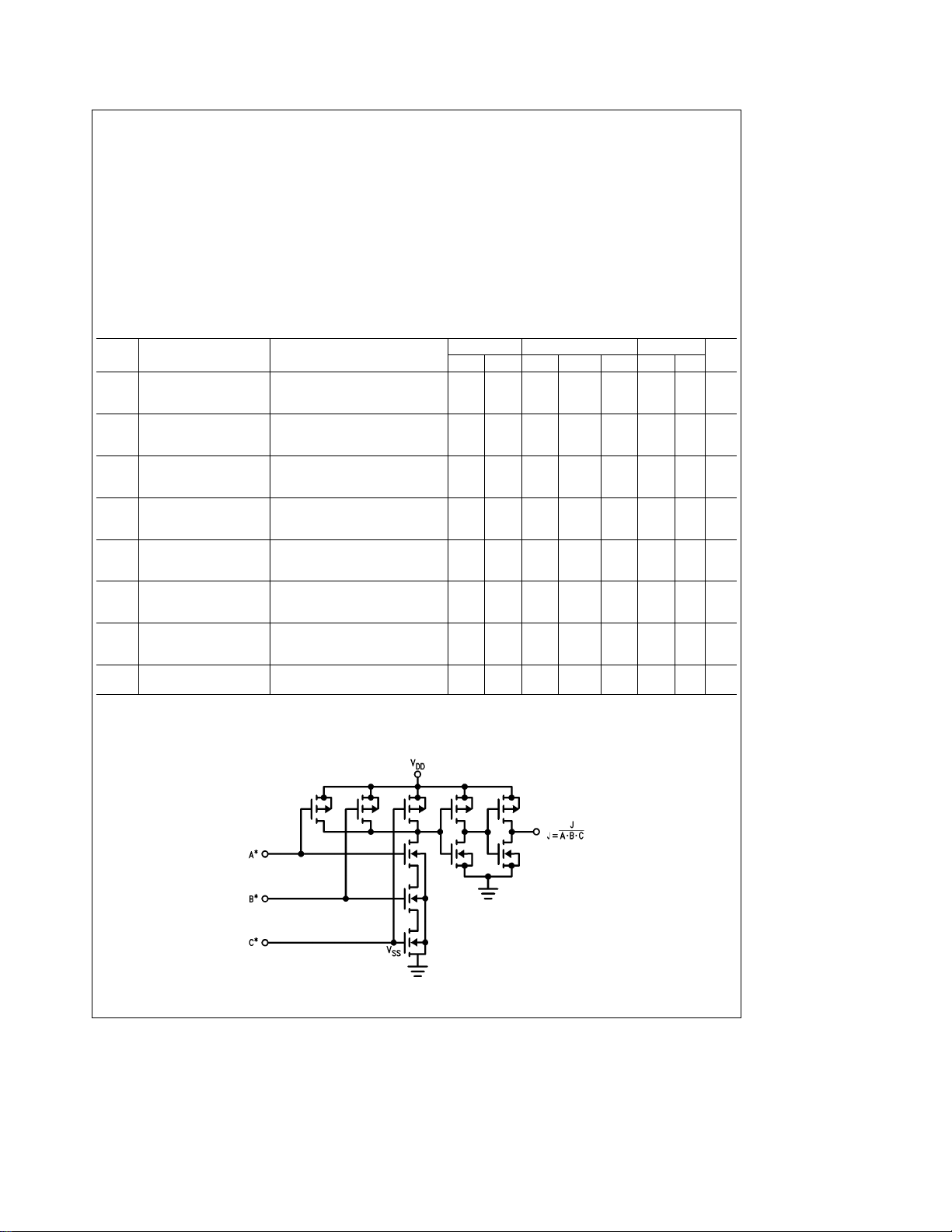
Schematic Diagram
CD4023BC/CD4023BM
2
(/3 Device Shown
*All Inputs Protected
by Standard CMOS Input
Protection Circuit.
TL/F/5956– 3
 Loading...