Motorola XC145481P, XC145481DW, XC145481D Datasheet

XC145481MOTOROLA
1
Product Preview
The XC145481 is a general purpose per channel PCM Codec–Filter with pin
selectable Mu–Law or A–Law companding, and is offered in 20–pin DIP, SOG,
and SSOP packages. This device performs the voice digitization and
reconstruction as well as the band limiting and smoothing required for PCM
systems. This device is designed to operate in both synchronous and
asynchronous applications and contains an on–chip precision reference
voltage.
This device has an input operational amplifier whose output is the input to the
encoder section. The encoder section immediately low–pass filters the analog
signal with an active R–C filter to eliminate very high frequency noise from being
modulated down to the passband by the switched capacitor filter. From the
active R–C filter, the analog signal is converted to a differential signal. From this
point, all analog signal processing is done differentially. This allows processing
of an analog signal that is twice the amplitude allowed by a single–ended
design, which reduces the significance of noise to both the inverted and
non–inverted signal paths. Another advantage of this differential design is that
noise injected via the power supplies is a common–mode signal that is
cancelled when the inverted and non–inverted signals are recombined. This
dramatically improves the power supply rejection ratio.
After the differential converter, a differential switched capacitor filter
bandpasses the analog signal from 200 Hz to 3400 Hz before the signal is
digitized by the differential compressing A/D converter.
The decoder accepts PCM data and expands it using a differential D/A
converter. The output of the D/A is low–pass filtered at 3400 Hz and sinX/X
compensated by a differential switched capacitor filter. The signal is then filtered
by an active R–C filter to eliminate the out of band energy of the switched
capacitor filter.
The XC145481 PCM Codec–Filter accepts a variety of clock formats,
including Short Frame Sync, Long Frame Sync, IDL, and GCI timing
environments.
The XC145481 PCM Codec–Filter utilizes CMOS due to its reliable
low–power performance and proven capability for complex analog/digital VLSI
functions.
• Single 3 V Power Supply
• Typical Power Dissipation of 12 mW, Power–Down of 0.01 mW
• Fully Differential Analog Circuit Design for Lowest Noise
• Transmit Band–Pass and Receive Low–Pass Filters On–Chip
• Active R–C Pre–Filtering and Post–Filtering
• Mu–Law and A–Law Companding by Pin Selection
• On–Chip Precision Reference Voltage (0.886 V) for a –5 dBm TLP @ 600 Ω
• Push–Pull 300 Ω Power Drivers with External Gain Adjust
This document contains information on a product under development. Motorola reserves the right to change or discontinue this product without notice.
Order this document
by XC145481/D
SEMICONDUCTOR TECHNICAL DATA
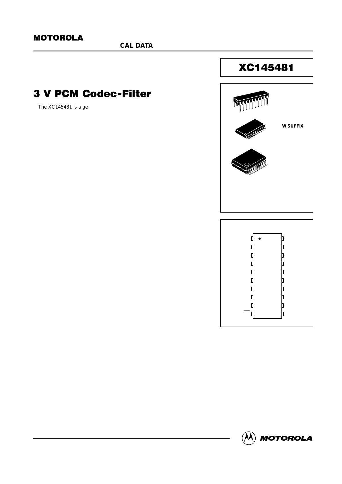
PIN ASSIGNMENT
P SUFFIX
PLASTIC DIP
CASE 738
DW SUFFIX
SOG PACKAGE
CASE 751D
ORDERING INFORMATION
XC145481P Plastic DIP
XC145481DW SOG Package
XC145481SD SSOP
20
1
20
1
SD SUFFIX
SSOP
CASE 940C
V
DD
PO–
PI
RO–
VAG–REF
PDI
BCLKR
DR
FSR
PO+ 5
4
3
2
1
10
9
8
7
6
14
15
16
17
18
19
20
11
12
13
Mu/A
TG
TI–
TI+
V
AG
MCLK
BCLKT
DT
FST
V
SS
20
1
Motorola, Inc. 1995
REV 0
10/95

XC145481 MOTOROLA
2
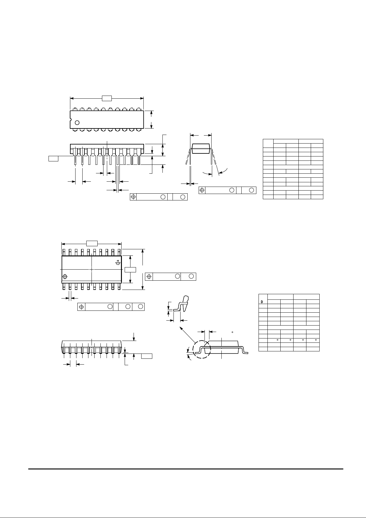
P ACKAGE DIMENSIONS
P SUFFIX
PLASTIC DIP
CASE 738–03
1.070
0.260
0.180
0.022
0.070
0.015
0.140
15°
0.040
1.010
0.240
0.150
0.015
0.050
0.008
0.110
0
°
0.020
25.66
6.10
3.81
0.39
1.27
0.21
2.80
0
°
0.51
27.17
6.60
4.57
0.55
1.77
0.38
3.55
15
°
1.01
0.050 BSC
0.100 BSC
0.300 BSC
1.27 BSC
2.54 BSC
7.62 BSC
MIN MINMAX MAX
INCHES MILLIMETERS
DIM
A
B
C
D
E
F
G
J
K
L
M
N
NOTES:
1. DIMENSIONING AND TOLERANCING PER ANSI
Y14.5M, 1982.
2. CONTROLLING DIMENSION: INCH.
3. DIMENSION L TO CENTER OF LEAD WHEN
FORMED PARALLEL.
4. DIMENSION B DOES NOT INCLUDE MOLD
FLASH.
-A-
C
K
N
E
GF
D
20 PL
J 20 PL
L
M
-T-
SEATING
PLANE
110
1120
0.25 (0.010) T A
M M
0.25 (0.010) T B
M M
B
DW SUFFIX
SOG PACKAGE
CASE 751D–04
NOTES:
1. DIMENSIONING AND TOLERANCING PER
ANSI Y14.5M, 1982.
2. CONTROLLING DIMENSION: MILLIMETER.
3. DIMENSIONS A AND B DO NOT INCLUDE
MOLD PROTRUSION.
4. MAXIMUM MOLD PROTRUSION 0.150
(0.006) PER SIDE.
5. DIMENSION D DOES NOT INCLUDE
DAMBAR PROTRUSION. ALLOWABLE
DAMBAR PROTRUSION SHALL BE 0.13
(0.005) TOTAL IN EXCESS OF D DIMENSION
AT MAXIMUM MATERIAL CONDITION.
–A–
–B–
20
1
11
10
S
A
M
0.010 (0.25) B
S
T
D20X
M
B
M
0.010 (0.25)
P10X
J
F
G
18X
K
C
–T–
SEATING
PLANE
M
R
X 45
_
DIM MIN MAX MIN MAX
INCHESMILLIMETERS
A 12.65 12.95 0.499 0.510
B 7.40 7.60 0.292 0.299
C 2.35 2.65 0.093 0.104
D 0.35 0.49 0.014 0.019
F 0.50 0.90 0.020 0.035
G 1.27 BSC 0.050 BSC
J 0.25 0.32 0.010 0.012
K 0.10 0.25 0.004 0.009
M 0 7 0 7
P 10.05 10.55 0.395 0.415
R 0.25 0.75 0.010 0.029
__
__
 Loading...