Motorola TL494CN, TL494CDR2, TL494CD, TL494IN Datasheet

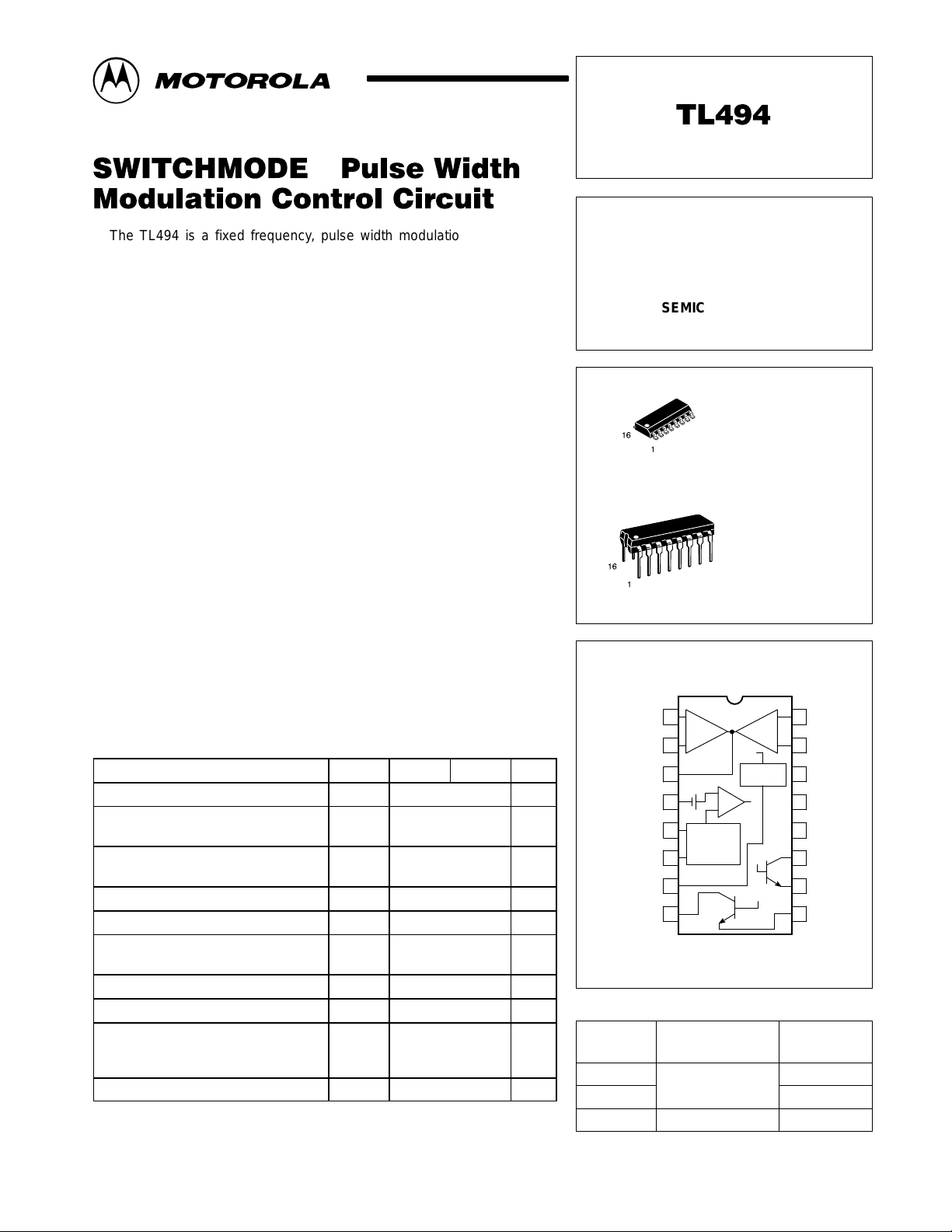
The TL494 is a fixed frequency, pulse width modulation control circuit
designed primarily for SWITCHMODE power supply control.
• Complete Pulse Width Modulation Control Circuitry
• On–Chip Oscillator with Master or Slave Operation
• On–Chip Error Amplifiers
• On–Chip 5.0 V Reference
• Adjustable Deadtime Control
• Uncommitted Output Transistors Rated to 500 mA Source or Sink
• Output Control for Push–Pull or Single–Ended Operation
• Undervoltage Lockout
Order this document by TL494/D
SWITCHMODE
PULSE WIDTH MODULATION
CONTROL CIRCUIT
SEMICONDUCTOR
TECHNICAL DATA
D SUFFIX
PLASTIC PACKAGE
CASE 751B
(SO–16)
MAXIMUM RATINGS
unless otherwise noted.)
Power Supply Voltage V
Collector Output Voltage VC1,
Collector Output Current
(Each transistor) (Note 1)
Amplifier Input Voltage Range V
Power Dissipation @ TA ≤ 45°C P
Thermal Resistance,
Junction–to–Ambient
Operating Junction Temperature T
Storage Temperature Range T
Operating Ambient Temperature Range
TL494C
TL494I
Derating Ambient Temperature T
NOTE: 1.Maximum thermal limits must be observed.
(Full operating ambient temperature range applies,
Rating Symbol TL494C TL494I Unit
IC1, I
N SUFFIX
PLASTIC PACKAGE
CASE 648
PIN CONNECTIONS
Noninv
1
Input
Input
Compen/PWN
CC
V
C2
C2
IR
D
R
θJA
J
stg
T
A
A
42 V
42 V
500 mA
–0.3 to +42 V
1000 mW
80 °C/W
125 °C
–55 to +125 °C
°C
0 to +70
–25 to +85
45 °C
Comp Input
Deadtime
Control
Ground
ORDERING INFORMATION
Device
TL494CD SO–16
TL494CN
TL494IN
+
Error
Amp
Inv
–
2
3
≈
0.1 V
4
C
5
T
Oscillator
R
6
T
7
C1
89
Operating
Temperature Range
TA = 0° to +70°C
TA = – 25° to +85°C
1
2
V
CC
Q1
(Top View)
Error
Amp
5.0 V
REF
+
–
Q2
Noninv
16
Input
Inv
15
Input
V
14
ref
Output
13
Control
V
12
CC
C2
11
E2
10
E1
Package
Plastic
Plastic
MOTOROLA ANALOG IC DEVICE DATA
Motorola, Inc. 1996 Rev 1
1

TL494
RECOMMENDED OPERATING CONDITIONS
Characteristics Symbol Min Typ Max Unit
Power Supply Voltage V
Collector Output Voltage VC1, V
Collector Output Current (Each transistor) IC1, I
Amplified Input Voltage V
Current Into Feedback Terminal l
Reference Output Current l
Timing Resistor R
Timing Capacitor C
Oscillator Frequency f
CC
fb
ref
osc
7.0 15 40 V
C2
C2
in
T
T
– 30 40 V
– – 200 mA
–0.3 – VCC – 2.0 V
– – 0.3 mA
– – 10 mA
1.8 30 500 kΩ
0.0047 0.001 10 µF
1.0 40 200 kHz
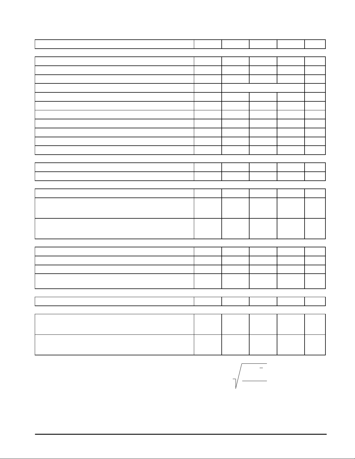
ELECTRICAL CHARACTERISTICS (V
For typical values TA = 25°C, for min/max values TA is the operating ambient temperature range that applies, unless otherwise noted.
Characteristics Symbol Min Typ Max Unit
REFERENCE SECTION
Reference Voltage (IO = 1.0 mA) V
Line Regulation (VCC = 7.0 V to 40 V) Reg
Load Regulation (IO = 1.0 mA to 10 mA) Reg
Short Circuit Output Current (V
OUTPUT SECTION
Collector Off–State Current
(VCC = 40 V, VCE = 40 V)
Emitter Off–State Current
VCC = 40 V, VC = 40 V, VE = 0 V)
Collector–Emitter Saturation Voltage (Note 2)
Common–Emitter (VE = 0 V, IC = 200 mA)
Emitter–Follower (VC = 15 V, IE = –200 mA)
Output Control Pin Current
Low State (VOC ≤ 0.4 V)
High State (VOC = V
Output Voltage Rise T ime
Common–Emitter (See Figure 12)
Emitter–Follower (See Figure 13)
Output Voltage Fall T ime
Common–Emitter (See Figure 12)
Emitter–Follower (See Figure 13)
NOTE: 2. Low duty cycle pulse techniques are used during test to maintain junction temperature as close to ambient temperature as possible.
ref
= 0 V) I
ref
)
= 15 V, CT = 0.01 µF, RT = 12 kΩ, unless otherwise noted.)
CC
4.75 5.0 5.25 V
– 2.0 25 mV
– 3.0 15 mV
15 35 75 mA
– 2.0 100 µA
– – –100 µA
–
–
–
–
–
–
–
–
I
C(off)
I
E(off)
V
sat(C)
V
sat(E)
I
OCL
I
OCH
ref
SC
t
t
line
load
r
f
1.1
1.5
10
0.2
100
100
25
40
1.3
2.5
–
3.5
200
200
100
100
V
µA
mA
ns
ns
2
MOTOROLA ANALOG IC DEVICE DATA

TL494
ELECTRICAL CHARACTERISTICS (V
For typical values TA = 25°C, for min/max values TA is the operating ambient temperature range that applies, unless otherwise noted.
Characteristics Symbol Min Typ Max Unit
ERROR AMPLIFIER SECTION
Input Offset Voltage (VO
Input Offset Current (VO
Input Bias Current (VO
Input Common Mode Voltage Range (VCC = 40 V, TA = 25°C) V
Open Loop Voltage Gain (∆VO = 3.0 V, VO = 0.5 V to 3.5 V, RL = 2.0 kΩ) A
Unity–Gain Crossover Frequency (VO = 0.5 V to 3.5 V, RL = 2.0 kΩ) f
Phase Margin at Unity–Gain (VO = 0.5 V to 3.5 V, RL = 2.0 kΩ) φ
Common Mode Rejection Ratio (VCC = 40 V) CMRR 65 90 – dB
Power Supply Rejection Ratio (∆VCC = 33 V, VO = 2.5 V, RL = 2.0 kΩ) PSRR – 100 – dB
Output Sink Current (VO
Output Source Current (VO
PWM COMPARATOR SECTION (Test Circuit Figure 11)
Input Threshold Voltage (Zero Duty Cycle) V
Input Sink Current (V
DEADTIME CONTROL SECTION (Test Circuit Figure 11)
Input Bias Current (Pin 4) (V
Maximum Duty Cycle, Each Output, Push–Pull Mode
(V
= 0 V, CT = 0.01 µF, RT = 12 kΩ)
Pin 4
(V
= 0 V, CT = 0.001 µF, RT = 30 kΩ)
Pin 4
Input Threshold Voltage (Pin 4)
(Zero Duty Cycle)
(Maximum Duty Cycle)
OSCILLATOR SECTION
Frequency (CT = 0.001 µF, RT = 30 kΩ) f
Standard Deviation of Frequency* (CT = 0.001 µF, RT = 30 kΩ) σf
Frequency Change with Voltage (VCC = 7.0 V to 40 V, TA = 25°C) ∆f
Frequency Change with Temperature (∆TA = T
(CT = 0.01 µF, RT = 12 kΩ)
UNDERVOLTAGE LOCKOUT SECTION
Turn–On Threshold (VCC increasing, I
TOTAL DEVICE
Standby Supply Current (Pin 6 at V
(VCC = 15 V)
(VCC = 40 V)
Average Supply Current
(CT = 0.01 µF, RT = 12 kΩ, V
(VCC = 15 V) (See Figure 12)
(Pin 3)
= 2.5 V) V
(Pin 3)
= 2.5 V) I
(Pin 3)
= 2.5 V) I
(Pin 3)
= 0.7 V) I
(Pin 3)
= 3.5 V) IO+ 2.0 –4.0 – mA
(Pin 3)
= 0.7 V) I
= 0 V to 5.25 V) IIB
Pin 4
, All other inputs and outputs open)
ref
(Pin 4)
= 15 V, CT = 0.01 µF, RT = 12 kΩ, unless otherwise noted.)
CC
IO
IO
IB
ICR
VOL
C–
m
O–
TH
I–
(DT)
DC
max
V
th
osc
osc
(∆V) – 0.1 – %
osc
to T
low
= 1.0 mA) V
ref
= 2.0 V)
high
)
∆f
(∆T) – – 12 %
osc
th
I
CC
– 2.0 10 mV
– 5.0 250 nA
– –0.1 –1.0 µA
–0.3 to VCC–2.0 V
70 95 – dB
– 350 – kHz
– 65 – deg.
0.3 0.7 – mA
– 2.5 4.5 V
0.3 0.7 – mA
– –2.0 –10 µA
45
–
–
0
– 40 – kHz
– 3.0 – %
5.5 6.43 7.0 V
–
–
– 7.0 –
48
45
2.8
–
5.5
7.0
50
50
3.3
–
10
15
%
V
mA
mA
* Standard deviation is a measure of the statistical distribution about the mean as derived from the formula, σ
MOTOROLA ANALOG IC DEVICE DATA
N
Σ (Xn – X
n = 1
N – 1
2
)
3

TL494
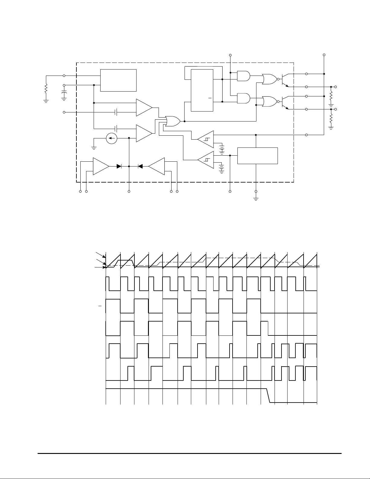
Figure 1. Representative Block Diagram
R
T
6
5
C
T
4
Deadtime
Control
Output Control
13
D
Ck
UV
Flip–
Flop
Q
Q
–
+
–
+
3.5V
4.9V
Ref.
Output
Reference
Regulator
Gnd
Oscillator
Deadtime
Comparator
0.12V
0.7V
0.7mA
+
1
–
12 3 1516 14 7
Error Amp
1
Feedback PWM
Comparator Input
–
+
–
+
PWM
Comparator
+
2
–
Error Amp
This device contains 46 active transistors.
Lockout
2
Q1
Q2
8
9
11
10
12
V
CC
V
CC
Capacitor C
Feedback/PWM Comp.
Deadtime Control
T
Flip–Flop
Clock Input
Flip–Flop
Q
Flip–Flop
Q
Output Q1
Emitter
Output Q2
Emitter
Output
Control
Figure 2. Timing Diagram
4
MOTOROLA ANALOG IC DEVICE DATA
 Loading...