

MOTOROLA TL431IP, TL431ILPRP, TL431ILPRA, TL431ID, TL431ILP Datasheet
...
Order this document by TL431/D
T
0° to +70°C
T
40° to +85°C
The TL431, A, B integrated circuits are three–terminal programmable
shunt regulator diodes. These monolithic IC voltage references operate as a
low temperature coefficient zener which is programmable from V
with two external resistors. These devices exhibit a wide operating current
range of 1.0 mA to 100 mA with a typical dynamic impedance of 0.22 Ω. The
characteristics of these references make them excellent replacements for
zener diodes in many applications such as digital voltmeters, power
supplies, and op amp circuitry. The 2.5 V reference makes it convenient to
obtain a stable reference from 5.0 V logic supplies, and since the TL431, A,
B operates as a shunt regulator, it can be used as either a positive or
negative voltage reference.
• Programmable Output Voltage to 36 V
• Voltage Reference Tolerance: ±0.4%, Typ @ 25°C (TL431B)
• Low Dynamic Output Impedance, 0.22 Ω Typical
• Sink Current Capability of 1.0 mA to 100 mA
• Equivalent Full–Range Temperature Coefficient of 50 ppm/°C Typical
• Temperature Compensated for Operation over Full Rated Operating
Temperature Range
• Low Output Noise Voltage
to 36 V
ref
PROGRAMMABLE
PRECISION REFERENCES
SEMICONDUCTOR
TECHNICAL DATA
LP SUFFIX
PLASTIC PACKAGE
CASE 29
(TO–92)
8
1
2
3
PLASTIC PACKAGE
1
Pin 1. Reference
2. Anode
3. Cathode
P SUFFIX
CASE 626
ORDERING INFORMATION
Operating
Device
TL431CLP, ACLP , BCLP
TL431CP, ACP, BCP
TL431CDM, ACDM, BCDM
TL431CD, ACD, BCD SOP–8
TL431ILP, AILP , BILP
TL431IP, AIP , BIP
TL431IDM, AIDM, BIDM
TL431ID, AID, BID SOP–8
Temperature Range
°
°
°
°
A
A
= –
=
–
Package
TO–92
Plastic
Micro–8
TO–92
Plastic
Micro–8
DM SUFFIX
8
1
Cathode
N/C
N/C
N/C
D SUFFIX
PLASTIC PACKAGE
CASE 751
(SOP–8)
Cathode
Anode Anode
N/C
SOP–8 is an internally modified SO–8 package. Pins 2,
3, 6 and 7 are electrically common to the die attach flag.
This internal lead frame modification decreases power
dissipation capability when appropriately mounted on a
printed circuit board. SOP–8 conforms to all external
dimensions of the standard SO–8 package.
PLASTIC PACKAGE
CASE 846A
(Micro–8)
1
2
3
4
(Top View)
1
2
3
4
8
7
6
5
8
8
7
6
5
(Top View)
Reference
N/C
Anode
N/C
1
Reference
N/C
MOTOROLA ANALOG IC DEVICE DATA
Motorola, Inc. 1999 Rev 7
1

TL431, A, B Series
Symbol
Cathode
(K)
Reference
(R)
Anode
(A)
Reference
(R)
Representative Block Diagram
Reference
(R)
2.5 V
+
–
ref
Anode (A)
Cathode
(K)
2.4 k 7.2 k
This device contains 12 active transistors.
MAXIMUM RATINGS (Full operating ambient temperature range applies, unless
otherwise noted.)
Rating
Cathode to Anode Voltage V
Cathode Current Range, Continuous I
Reference Input Current Range, Continuous I
Operating Junction Temperature T
Operating Ambient Temperature Range T
TL431I, TL431AI, TL431BI –40 to +85
TL431C, TL431AC, TL431BC 0 to +70
Storage Temperature Range T
Total Power Dissipation @ TA = 25°C P
Derate above 25°C Ambient Temperature
D, LP Suffix Plastic Package 0.70
P Suffix Plastic Package 1.10
DM Suffix Plastic Package 0.52
Total Power Dissipation @ TC = 25°C P
Derate above 25°C Case Temperature
D, LP Suffix Plastic Package 1.5
P Suffix Plastic Package 3.0
NOTE: ESD data available upon request.
Symbol Value Unit
KA
K
ref
J
37 V
–100 to +150 mA
–0.05 to +10 mA
150 °C
A
stg
–65 to +150 °C
D
D
Representative Schematic Diagram
Component values are nominal
Cathode (K)
800
20 pF
150
10 k
1.0 k
3.28 k
°C
W
W
800
20 pF
800
4.0 k
Anode (A)
RECOMMENDED OPERATING CONDITIONS
Condition Symbol Min Max Unit
Cathode to Anode Voltage V
Cathode Current I
THERMAL CHARACTERISTICS
D, LP Suffix
Characteristic Symbol
Thermal Resistance, Junction–to–Ambient R
Thermal Resistance, Junction–to–Case R
θJA
θJC
Package
2
KA
K
V
ref
1.0 100 mA
P Suffix
Package
36 V
DM Suffix
Package
Unit
178 114 240 °C/W
83 41 – °C/W
MOTOROLA ANALOG IC DEVICE DATA

TL431, A, B Series
ref
D
V
ELECTRICAL CHARACTERISTICS (T
= 25°C, unless otherwise noted.)
A
TL431I TL431C
Characteristic Symbol
Reference Input Voltage (Figure 1) V
VKA = V
, IK = 10 mA
ref
ref
Min Typ Max Min Typ Max Unit
TA = 25°C 2.44 2.495 2.55 2.44 2.495 2.55
TA = T
Reference Input Voltage Deviation Over ∆V
low
to T
(Note 1) 2.41 – 2.58 2.423 – 2.567
high
ref
– 7.0 30 – 3.0 17 mV
Temperature Range (Figure 1, Notes 1, 2)
VKA= V
Ratio of Change in Reference Input Voltage
to Change in Cathode to Anode Voltage
IK = 10 mA (Figure 2),
∆VKA = 10 V to V
ref, IK
= 10 mA
ref
D
V
D
V
KA
– –1.4 –2.7 – –1.4 –2.7
∆VKA = 36 V to 10 V – –1.0 –2.0 – –1.0 –2.0
Reference Input Current (Figure 2) I
ref
IK = 10 mA, R1 = 10 k, R2 = ∞
TA = 25°C – 1.8 4.0 – 1.8 4.0
TA = T
Reference Input Current Deviation Over ∆I
low
to T
(Note 1) – – 6.5 – – 5.2
high
ref
– 0.8 2.5 – 0.4 1.2 µA
Temperature Range (Figure 2, Note 1, 4)
IK = 10 mA, R1 = 10 k, R2 = ∞
Minimum Cathode Current For Regulation I
VKA = V
(Figure 1)
ref
Off–State Cathode Current (Figure 3) I
VKA = 36 V, V
ref
= 0 V
min
off
– 0.5 1.0 – 0.5 1.0 mA
– 260 1000 – 260 1000 nA
Dynamic Impedance (Figure 1, Note 3) |ZKA| – 0.22 0.5 – 0.22 0.5 Ω
VKA = V
, ∆IK = 1.0 mA to 100 mA
ref
f ≤ 1.0 kHz
NOTES: 1. T
= –40°C for TL431AIP TL431AILP, TL431IP, TL431ILP, TL431BID, TL431BIP, TL431BILP, TL431AIDM, TL431IDM, TL431BIDM
low
=0°C for TL431ACP, TL431ACLP, TL431CP , TL431CLP, TL431CD, TL431ACD, TL431BCD, TL431BCP , TL431BCLP, TL431CDM,
TL431ACDM, TL431BCDM
T
= +85°C for TL431AIP, TL431AILP, TL431IP, TL431ILP, TL431BID, TL431BIP, TL431BILP, TL431IDM, TL431AIDM, TL431BIDM
high
= +70°C for TL431ACP, TL431ACLP, TL431CP, TL431ACD, TL431BCD, TL431BCP, TL431BCLP , TL431CDM, TL431ACDM, TL431BCDM
2.The deviation parameter ∆V
temperature range that applies.
is defined as the difference between the maximum and minimum values obtained over the full operating ambient
ref
V
mV/V
µA
The average temperature coefficient of the reference input voltage, αV
V
ref
αV
can be positive or negative depending on whether V
ref
3.The dynamic impedance ZKA is defined as
When the device is programmed with two external resistors, R1 and R2, (refer to Figure 2) the total dynamic impedance of the circuit is defined as:
Example :DV
+
8.0 mV and slope is positive,
ref
V
@25_C+2.495 V,DTA+70_
ref
MOTOROLA ANALOG IC DEVICE DATA
V
ref
V
ref
ppm
_
|ZKA|
C
max
min
+
T1
ǒ
V
D
+
Ambient T emperature
ref
D
V
ref
X10
Ǔ
@25_C
ref
D
T
A
Min or V
ref
V
KA
D
I
K
|ZKAȀ|[
ref
C
|ZKA|ǒ1
∆
V
= V
max
ref
ref
–V
min
ref
∆
TA = T2 – T
1
T2
is defined as:
6
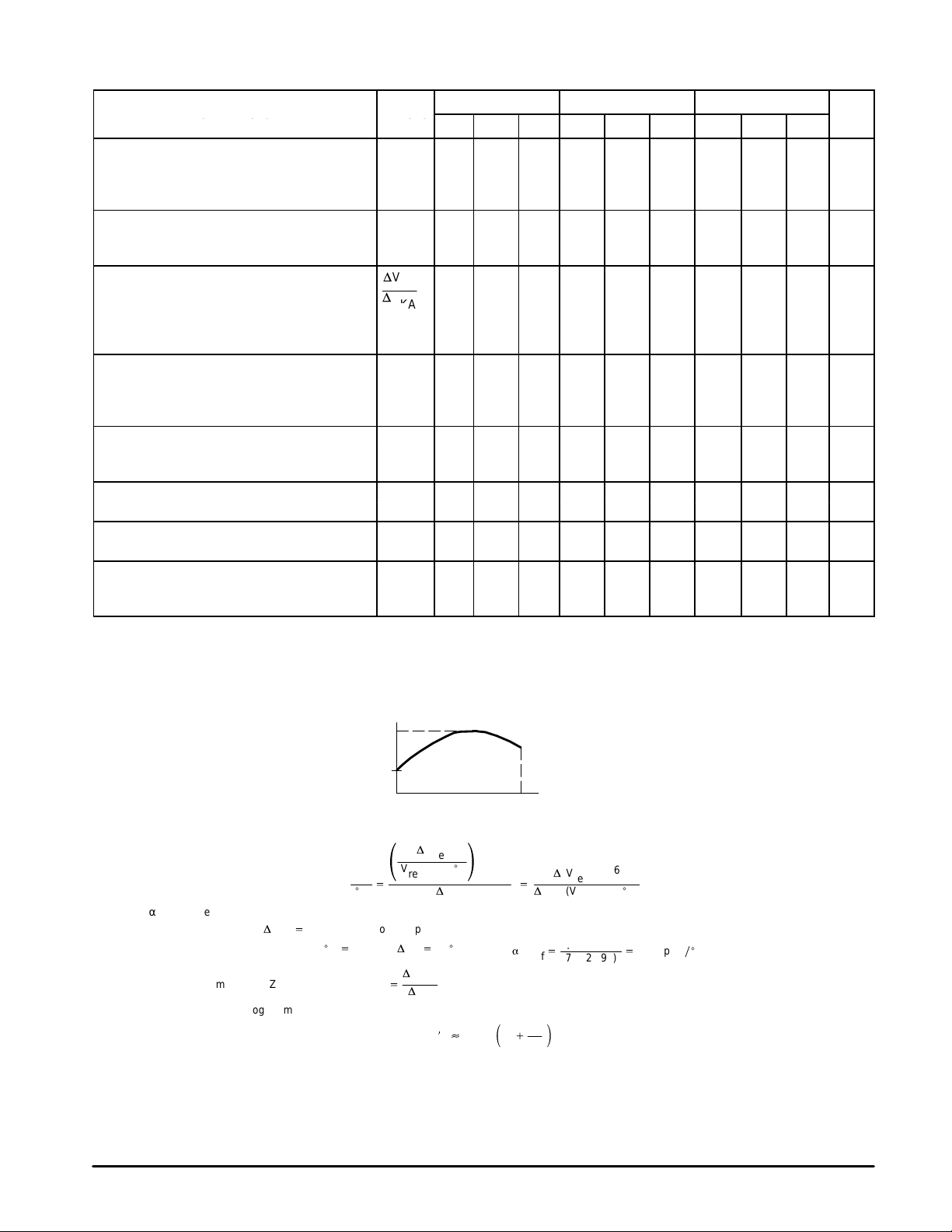
Max occurs at the lower ambient temperature. (Refer to Figure 6.)
D
V
R1
R2
D
ref
V
TA(V
0.008 x 10
+
70 (2.495)
Ǔ
+
a
)
ref
ref
6
x10
@25_C)
6
+
45.8 ppmń_
C
3
TL431, A, B Series
ref
D
V
ELECTRICAL CHARACTERISTICS (T
= 25°C, unless otherwise noted.)
A
TL431AI TL431AC TL431BI
Characteristic Symbol
Reference Input Voltage (Figure 1) V
VKA = V
, IK = 10 mA
ref
Min Typ Max Min Typ Max Min Typ Max Unit
ref
TA = 25°C 2.47 2.495 2.52 2.47 2.495 2.52 2.483 2.495 2.507
TA = T
Reference Input Voltage Deviation Over ∆V
low
to T
high
2.44 – 2.55 2.453 – 2.537 2.475 2.495 2.515
– 7.0 30 – 3.0 17 – 3.0 17 mV
ref
Temperature Range (Figure 1, Notes 1, 2)
VKA= V
Ratio of Change in Reference Input Voltage
to Change in Cathode to Anode Voltage
IK = 10 mA (Figure 2),
∆VKA = 10 V to V
ref, IK
= 10 mA
ref
D
V
D
V
KA
– –1.4 –2.7 – –1.4 –2.7 – –1.4 –2.7
∆VKA = 36 V to 10 V – –1.0 –2.0 – –1.0 –2.0 – –1.0 –2.0
Reference Input Current (Figure 2) I
ref
IK = 10 mA, R1 = 10 k, R2 = ∞
TA = 25°C – 1.8 4.0 – 1.8 4.0 – 1.1 2.0
TA = T
Reference Input Current Deviation Over ∆I
low
to T
(Note 1) – – 6.5 – – 5.2 – – 4.0
high
ref
– 0.8 2.5 – 0.4 1.2 – 0.8 2.5 µA
Temperature Range (Figure 2, Note 1)
IK = 10 mA, R1 = 10 k, R2 = ∞
Minimum Cathode Current For Regulation I
VKA = V
(Figure 1)
ref
Off–State Cathode Current (Figure 3) I
VKA = 36 V, V
ref
= 0 V
min
off
– 0.5 1.0 – 0.5 1.0 – 0.5 1.0 mA
– 260 1000 – 260 1000 – 230 500 nA
Dynamic Impedance (Figure 1, Note 3) |ZKA| – 0.22 0.5 – 0.22 0.5 – 0.14 0.3 Ω
VKA = V
, ∆IK = 1.0 mA to 100 mA
ref
f ≤ 1.0 kHz
NOTES: 1. T
= –40°C for TL431AIP TL431AILP, TL431IP, TL431ILP, TL431BID, TL431BIP, TL431BILP, TL431AIDM, TL431IDM, TL431BIDM
low
=0°C for TL431ACP, TL431ACLP, TL431CP , TL431CLP, TL431CD, TL431ACD, TL431BCD, TL431BCP , TL431BCLP, TL431CDM,
TL431ACDM, TL431BCDM
T
= +85°C for TL431AIP, TL431AILP, TL431IP, TL431ILP, TL431BID, TL431BIP, TL431BILP, TL431IDM, TL431AIDM, TL431BIDM
high
= +70°C for TL431ACP, TL431ACLP, TL431CP, TL431ACD, TL431BCD, TL431BCP, TL431BCLP , TL431CDM, TL431ACDM, TL431BCDM
2.The deviation parameter ∆V
temperature range that applies.
is defined as the difference between the maximum and minimum values obtained over the full operating ambient
ref
V
max
ref
V
min
ref
∆
V
= V
ref
–V
min
ref
∆
TA = T2 – T
ref
max
1
V
mV/V
µA
T1
Ambient T emperature
The average temperature coefficient of the reference input voltage, αV
D
V
ref
ǒ
V
ppm
V
ref
_
C
αV
can be positive or negative depending on whether V
ref
3.The dynamic impedance ZKA is defined as
When the device is programmed with two external resistors, R1 and R2, (refer to Figure 2) the total dynamic impedance of the circuit is defined as:
Example :DV
+
8.0 mV and slope is positive,
ref
V
@25_C+2.495 V,DTA+70_
ref
|ZKA|
ref
+
D
V
+
D
|ZKAȀ|[
@25_C
D
Min or V
ref
KA
I
K
Ǔ
T
A
C
|ZKA|ǒ1
4
T2
is defined as:
ref
6
X10
Max occurs at the lower ambient temperature. (Refer to Figure 6.)
ref
D
V
R1
R2
D
ref
V
TA(V
0.008 x 10
+
70 (2.495)
Ǔ
+
a
)
ref
ref
6
x10
@25_C)
6
+
45.8 ppmń_
C
MOTOROLA ANALOG IC DEVICE DATA

TL431, A, B Series
0
5
Figure 1. Test Circuit for VKA = V
Input
V
ref
V
KA
I
K
Figure 4. Cathode Current versus
Cathode Voltage
ref
°
C
KA
I
K
, CATHODE CURRENT (mA)
K
I
150
100
Input V
50
0
–50
VKA = V
TA = 25
ref
Figure 2. Test Circuit for VKA > V
I
K
VKA+
V
KA
R1
ǒ
V
1
)
ref
R2
Input
R1
R2
I
ref
V
ref
Figure 5. Cathode Current versus
800
600
Input
µ
400
200
, CATHODE CURRENT ( A)
0
K
I
ref
Ǔ
)
I
ref
VKA = V
TA = 25
Figure 3. T est Circuit for I
S
R1
Cathode Voltage
ref
°
C
V
KA
I
K
Input V
I
I
off
Min
off
KA
–100
–2.0 –1.0 0
Figure 6. Reference Input V oltage versus
2600
Input
2580
2560
2540
2520
2500
2480
2460
2440
2420
ref
V , REFERENCE INPUT VOLTAGE (mV)
2400
–55
V
ref
TA, AMBIENT TEMPERATURE (
1.0 2.0 3.0
VKA, CATHODE VOLTAGE (V)
Ambient Temperature
V
KA
I
VKA = V
K
ref
IK = 10 mA
050
25–25
V
Max = 2550 mV
ref
V
Typ = 2495 mV
ref
V
Min = 2440 mV
ref
75 100 125
°
C)
–200
µ
, REFERENCE INPUT CURRENT ( A)
ref
I
–1.0
0
1.0 2.0 3.
VKA, CATHODE VOLTAGE (V)
Figure 7. Reference Input Current versus
Ambient Temperature
3.0
2.5
2.0
1.5
IK = 10 mA
1.0
0.5
Input
I
ref
10k
0
V
KA
I
K
250–25
TA, AMBIENT TEMPERATURE (°C)
12
10050 75–55
MOTOROLA ANALOG IC DEVICE DATA
5
 Loading...