

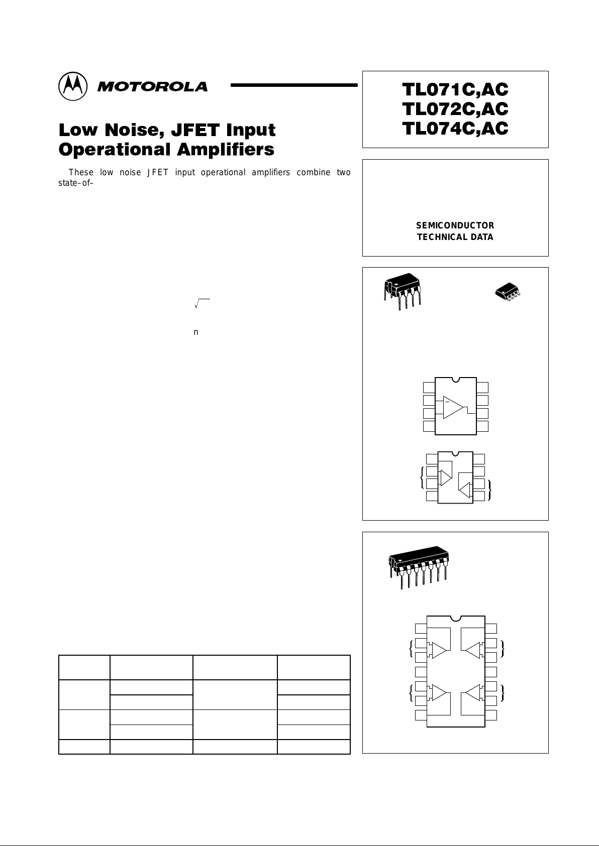
TL071 (Top View)
TL072 (Top View)
TL074 (Top View)
D SUFFIX
PLASTIC PACKAGE
CASE 751
(SO–8)
P SUFFIX
PLASTIC PACKAGE
CASE 626
N SUFFIX
PLASTIC PACKAGE
CASE 646
(TL074 Only)
1
1
8
8
PIN CONNECTIONS
PIN CONNECTIONS
4
23
1
+
14
1
Offset Null
Noninvt Input
V
EE
Inv + Input
V
EE
Inputs A
Output A
Inputs 1
Output 1
V
CC
Inputs 2
Output 2
NC
V
CC
Output
Offset Null
Inputs B
Output B
V
CC
Output 4
Inputs 4
V
EE
Inputs 3
Output 3
–
–
+
+
–
–
––
+
+
++
18
7
6
5
2
3
4
18
7
6
5
2
3
4
114
13
12
11
10
9
8
2
3
4
5
6
7
SEMICONDUCTOR
TECHNICAL DATA
LOW NOISE, JFET INPUT
OPERATIONAL AMPLIFIERS
Order this document by TL071C/D
1
MOTOROLA ANALOG IC DEVICE DATA
These low noise JFET input operational amplifiers combine two
state–of–the–art analog technologies on a single monolithic integrated
circuit. Each internally compensated operational amplifier has well matched
high voltage JFET input device for low input offset voltage. The BIFET
technology provides wide bandwidths and fast slew rates with low input bias
currents, input offset currents, and supply currents. Moreover, the devices
exhibit low noise and low harmonic distortion, making them ideal for use in
high fidelity audio amplifier applications.
These devices are available in single, dual and quad operational
amplifiers which are pin–compatible with the industry standard MC1741,
MC1458, and the MC3403/LM324 bipolar products.
• Low Input Noise Voltage: 18 nV/ Hz
Ǹ
Typ
• Low Harmonic Distortion: 0.01% Typ
• Low Input Bias and Offset Currents
• High Input Impedance: 10
12
Ω Typ
• High Slew Rate: 13 V/µs Typ
• Wide Gain Bandwidth: 4.0 MHz Typ
• Low Supply Current: 1.4 mA per Amp
ORDERING INFORMATION
Op Amp
Function
Device
Operating
Temperature Range
Package
TL071CD
°
°
SO–8
Single
TL071ACP
T
A
= 0° to +
70°C
Plastic DIP
TL072CD
°
°
SO–8
Dual
TL072ACP
T
A
= 0° to +
70°C
Plastic DIP
Quad TL074CN, ACN TA = 0° to +70°C Plastic DIP
Motorola, Inc. 1997 Rev 1
TL071C,AC TL072C,AC TL074C,AC
2
MOTOROLA ANALOG IC DEVICE DATA
MAXIMUM RATINGS
Rating Symbol Value Unit
Supply Voltage V
CC
18 V
V
EE
–18
Differential Input Voltage V
ID
±30 V
Input Voltage Range (Note 1) V
IDR
±15 V
Output Short Circuit Duration (Note 2) t
SC
Continuous
Power Dissipation
Plastic Package (N, P) P
D
680 mW
Derate above TA = 47°C 1.0/θ
JA
10 mW/°C
Operating Ambient Temperature Range T
A
0 to +70 °C
Storage Temperature Range T
stg
–65 to +150 °C
NOTES: 1. The magnitude of the input voltage must not exceed the magnitude of the supply voltage or
15 V, whichever is less.
2.The output may be shorted to ground or either supply. Temperature and/or supply voltages
must be limited to ensure that power dissipation ratings are not exceeded.
3.ESD data available upon request.
ELECTRICAL CHARACTERISTICS (V
CC
= 15 V, VEE = –15 V , TA = T
high
to T
low
[Note 1])
Characteristics Symbol Min Typ Max Unit
Input Offset Voltage (RS ≤ 10 k, VCM = 0) V
IO
mV
TL071C, TL072C – – 13
TL074C – – 13
TL07_AC – – 7.5
Input Offset Current (VCM = 0) (Note 2) I
IO
nA
TL07_C – – 2.0
TL07_AC – – 2.0
Input Bias Current (VCM = 0) (Note 2) I
IB
nA
TL07_C – – 7.0
TL07_AC – – 7.0
Large–Signal Voltage Gain (VO = ±10 V, RL ≥ 2.0 k) A
VOL
V/mV
TL07_C 15 – –
TL07_AC 25 – –
Output Voltage Swing (Peak–to–Peak) V
O
V
(RL ≥ 10 k) 24 – –
(RL ≥ 2.0 k) 20 – –
NOTES: 1. T
low
=0°C for TL071C,AC T
high
=70°C for TL071C,AC
0°C for TL072C,AC T
high
=70°C for TL072C,AC
0°C for TL074C,AC T
high
=70°C for TL074C,AC
2.Input Bias currents of JFET input op amps approximately double for every 10°C rise in junction temperature as shown in Figure 3. To maintain
junction temperature as close to ambient temperature as possible, pulse techniques must be used during testing.
Figure 1. Unity Gain Voltage Follower Figure 2. Inverting Gain of 10 Amplifier
–
+
V
in
RL = 2.0 k
V
O
CL = 100 pF
–
+
V
in
R
L
V
O
CL = 100 pF
10 k
1.0 k
TL071C,AC TL072C,AC TL074C,AC
3
MOTOROLA ANALOG IC DEVICE DATA
ELECTRICAL CHARACTERISTICS (V
CC
= 15 V, VEE = –15 V , TA = 25°C, unless otherwise noted.)
Characteristics Symbol Min Typ Max Unit
Input Offset Voltage (RS ≤ 10 k, VCM = 0) V
IO
mV
TL071C, TL072C – 3.0 10
TL074C – 3.0 10
TL07_AC – 3.0 6.0
Average Temperature Coefficient of Input Of fset Voltage ∆VIO/∆T – 10 – µV/°C
RS = 50 Ω, TA = T
low
to T
high
(Note 1)
Input Offset Current (VCM = 0) (Note 2) I
IO
pA
TL07_C – 5.0 50
TL07_AC – 5.0 50
Input Bias Current (VCM = 0) (Note 2) I
IB
pA
TL07_C – 30 200
TL07_AC – 30 200
Input Resistance r
i
– 10
12
– Ω
Common Mode Input Voltage Range V
ICR
V
TL07_C ±10 15, –12 –
TL07_AC ±11 15, –12 –
Large–Signal Voltage Gain (VO = ±10 V, RL ≥ 2.0 k) A
VOL
V/mV
TL07_C 25 150 –
TL07_AC 50 150 –
Output Voltage Swing (Peak–to–Peak) V
O
24 28 – V
(RL = 10 k)
Common Mode Rejection Ratio (RS ≤ 10 k) CMRR dB
TL07_C 70 100 –
TL07_AC 80 100 –
Supply Voltage Rejection Ratio (RS ≤ 10 k) PSRR dB
TL07_C 70 100 –
TL07_AC 80 100 –
Supply Current (Each Amplifier) I
D
– 1.4 2.5 mA
Unity Gain Bandwidth BW – 4.0 – MHz
Slew Rate (See Figure 1) SR – 13 – v/µs
Vin = 10 V, RL = 2.0 k, CL = 100 pF
Rise Time (See Figure 1) t
r
– 0.1 – µs
Overshoot (Vin = 20 mV, RL = 2.0 k, CL = 100 pF) OS – 10 – %
Equivalent Input Noise Voltage e
n
– 18 –
nV/ Hz√
RS = 100 Ω, f = 1000 Hz
Equivalent Input Noise Current i
n
– 0.01 –
pA/ Hz√
RS = 100 Ω, f = 1000 Hz
Total Harmonic Distortion THD – 0.01 – %
VO (RMS) = 10 V, RS ≤ 1.0 k, RL ≥ 2.0 k, f = 1000 Hz
Channel Separation CS – 120 – dB
AV = 100
NOTES: 1. T
low
=0°C for TL071C,AC T
high
=70°C for TL071C,AC
0°C for TL072C,AC T
high
=70°C for TL072C,AC
0°C for TL074C,AC T
high
=70°C for TL074C,AC
2. Input Bias currents of JFET input op amps approximately double for every 10°C rise in junction temperature as shown in Figure 3. To maintain
junction temperature as close to ambient temperature as possible, pulse techniques must be used during testing.

TL071C,AC TL072C,AC TL074C,AC
4
MOTOROLA ANALOG IC DEVICE DATA
V
O
, OUTPUT VOL TAGE SWING (V
pp
)
V
O
, OUTPUT VOL TAGE SWING (V
pp
)
V
O
, OUTPUT VOL TAGE SWING (V
pp
)
V
O
, OUTPUT VOL TAGE SWING (V
pp
)
VCC/VEE = ±15 V
(See Figure 2)
RL = 10 k
RL = 2.0 k
Figure 3. Input Bias Current
versus Temperature
Figure 4. Output Voltage Swing
versus Frequency
Figure 5. Output Voltage Swing
versus Load Resistance
Figure 6. Output Voltage Swing
versus Supply Voltage
Figure 7. Output Voltage Swing
versus Temperature
Figure 8. Supply Current per Amplifier
versus Temperature
TA, AMBIENT TEMPERATURE (°C)
IB
–75 –50 –25 0 25 50 75 100 125
VCC/VEE = ±15 V
100 1.0 k 10 k 100 k 1.0 M 10 M
f, FREQUENCY (Hz)
RL, LOAD RESISTANCE (kΩ)
0.1 0.2 0.4 0.7 1.0 2.0 104.0 7.0
VCC, |VEE| , SUPPLY VOLT AGE (±V)
0 5.0 10 15 20
RL = 2.0 k
TA = 25
°
C
TA, AMBIENT TEMPERATURE (
°
C)
–50 –25 0 25 50 75 100 125
TA, AMBIENT TEMPERATURE (°C)
–50 –25 0 25 50 75 100 125
I
D
VCC/VEE = ±15 V
TA = 25
°
C
(See Figure 2)
0.6
100
10
1.0
0.1
0.01
30
25
20
15
10
5.0
0
30
20
10
5.0
0
40
30
20
10
0
35
30
25
20
15
10
5.0
0
2.0
1.8
1.6
1.4
1.2
1.0
0.8
0.4
0.2
0
VCC/VEE = ±15 V
±
10 V
±
5.0 V
RL = 2.0 k
TA = 25
°
C
(See Figure 2)
VCC/VEE = ±15 V
I , INPUT BIAS CURRENT (nA)
, SUPPLY DRAIN CURRENT (mA)
–100 150
35
40
40
–75 –75
TL071C,AC TL072C,AC TL074C,AC
5
MOTOROLA ANALOG IC DEVICE DATA
, VOLTAGE GAIN (V/mV)
VOL
V
, EQUIVALENT INPUT NOISE VOLTAGE (
Figure 9. Large Signal Voltage Gain and
Phase Shift versus Frequency
Figure 10. Large Signal Voltage Gain
versus Temperature
Figure 11. Normalized Slew Rate
versus Temperature
Figure 12. Equivalent Input Noise Voltage
versus Frequency
Figure 13. Total Harmonic Distortion
versus Frequency
f, FREQUENCY (Hz)
PHASE SHIFT (DEGREES)
10
6
10
5
10
4
10
3
10
1
10
2
1.0
1.0 10 100 1.0 k 10 k 100 k 1.0 M 10 M
, OPEN–LOOP GAIN
VOL
Gain
Phase Shift
VCC/VEE = ±15 V
RL = 2.0 k
TA = 25
°
C
VCC/VEE = ±15 V
VO =
±
10 V
RL = 2.0 k
TA, AMBIENT TEMPERATURE (
°
C)
1000
100
10
1.0
–50 –25 0 25 50 75 100 125
TA, AMBIENT TEMPERATURE (
°
C)
NORMALIZED SLEW RATE
1.15
1.10
1.05
1.0
0.95
0.90
0.85
–50 –25 0 25 50 75 100 125
f, FREQUENCY (Hz)
60
50
40
30
20
10
0
0.01 0.05 0.1 0.5 1.0 5.0 10 50 100
VCC/VEE = ±15 Vdc
AV = 10
RS = 100
Ω
TA = 25°C
VCC/VEE = ±15 V
AV = 1.0
VO = 6.0 V (RMS)
TA = 25
°
C
f, FREQUENCY (Hz)
THD, TOT AL HARMONIC DISTORTION (%)
1.0
0.5
0.1
0.05
0.01
0.005
0.001
0.1 0.5 1.0 5.0 10 50 100
0
°
45
°
90
°
135
°
180
°
V
e
nV/ Hz√
n
)
10
7
10
8
100 M –75–100 150
1.20
0.80
–75
70

TL071C,AC TL072C,AC TL074C,AC
6
MOTOROLA ANALOG IC DEVICE DATA
Representative Schematic Diagram
(Each Amplifier)
–
+
Inputs
Q3
Q4 Q5
Q2
Q1
V
CC
Q6
J1 J2
Q17
Q20
Q23
24
J3
2.0 k
Q14
Q15
10 pF
Q19
Q21
Q22
Q24
Q9
Q8
Q7
Q25
Q12
Q10
Q13
Q11
Q16
Q18
1.5 k
V
EE
Bias Circuitry
Common to All
Amplifiers
Offset
Null
(TL071
only)
Output
1.5 k
Figure 14. Audio Tone Control Amplifier
Figure 15. High Q Notch Filter
Turn–Over Frequency = 1.0 kHz
Bass Boost/Cut —
±
20 dB at 20 Hz
Treble Boost/Cut —
±
19 dB at 20 kHz
Input
0.033
µ
F
10 k
V
CC
TL071
V
EE
Output
3.3 k
–
+
10 k
10 k
0.033
µ
F
68 k
0.033
µ
F 0.033 µF
100 k
Input
RR
C1
R1
C
C
TL071
+
–
100 k
fo+
1
2
p
RC
+
350 Hz
R+2R1+1.5 M
C
+
C1
2
+
300 pF

TL071C,AC TL072C,AC TL074C,AC
7
MOTOROLA ANALOG IC DEVICE DATA
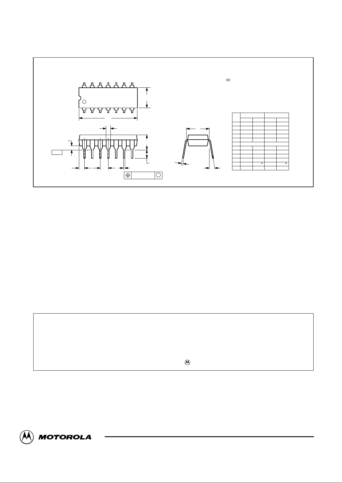
OUTLINE DIMENSIONS
P SUFFIX
PLASTIC PACKAGE
CASE 626–05
ISSUE K
14
58
F
NOTE 2
–A–
–B–
–T–
SEATING
PLANE
H
J
G
D
K
N
C
L
M
M
A
M
0.13 (0.005) B
M
T
NOTES:
1. DIMENSION L TO CENTER OF LEAD WHEN
FORMED PARALLEL.
2. PACKAGE CONTOUR OPTIONAL (ROUND OR
SQUARE CORNERS).
3. DIMENSIONING AND TOLERANCING PER ANSI
Y14.5M, 1982.
DIM MIN MAX MIN MAX
INCHESMILLIMETERS
A 9.40 10.16 0.370 0.400
B 6.10 6.60 0.240 0.260
C 3.94 4.45 0.155 0.175
D 0.38 0.51 0.015 0.020
F 1.02 1.78 0.040 0.070
G 2.54 BSC 0.100 BSC
H 0.76 1.27 0.030 0.050
J 0.20 0.30 0.008 0.012
K 2.92 3.43 0.115 0.135
L 7.62 BSC 0.300 BSC
M ––– 10 ––– 10
N 0.76 1.01 0.030 0.040
__
D SUFFIX
PLASTIC PACKAGE
CASE 751–05
(SO–8)
ISSUE S
SEATING
PLANE
1
4
58
A0.25MCB
SS
0.25MB
M
h
q
C
X 45
_
L
DIM MIN MAX
MILLIMETERS
A 1.35 1.75
A1 0.10 0.25
B 0.35 0.49
C 0.18 0.25
D 4.80 5.00
E
1.27 BSCe
3.80 4.00
H 5.80 6.20
h
0 7
L 0.40 1.25
q
0.25 0.50
__
NOTES:
1. DIMENSIONING AND TOLERANCING PER ASME
Y14.5M, 1994.
2. DIMENSIONS ARE IN MILLIMETERS.
3. DIMENSION D AND E DO NOT INCLUDE MOLD
PROTRUSION.
4. MAXIMUM MOLD PROTRUSION 0.15 PER SIDE.
5. DIMENSION B DOES NOT INCLUDE MOLD
PROTRUSION. ALLOWABLE DAMBAR
PROTRUSION SHALL BE 0.127 TOTAL IN EXCESS
OF THE B DIMENSION AT MAXIMUM MATERIAL
CONDITION.
D
E
H
A
B
e
B
A1
C
A
0.10
TL071C,AC TL072C,AC TL074C,AC
8
MOTOROLA ANALOG IC DEVICE DATA
OUTLINE DIMENSIONS
N SUFFIX
PLASTIC PACKAGE
CASE 646–06
ISSUE M
17
14 8
B
A
DIM MIN MAX MIN MAX
MILLIMETERSINCHES
A 0.715 0.770 18.16 18.80
B 0.240 0.260 6.10 6.60
C 0.145 0.185 3.69 4.69
D 0.015 0.021 0.38 0.53
F 0.040 0.070 1.02 1.78
G 0.100 BSC 2.54 BSC
H 0.052 0.095 1.32 2.41
J 0.008 0.015 0.20 0.38
K 0.115 0.135 2.92 3.43
L
M ––– 10 ––– 10
N 0.015 0.039 0.38 1.01
__
NOTES:
1. DIMENSIONING AND TOLERANCING PER ANSI
Y14.5M, 1982.
2. CONTROLLING DIMENSION: INCH.
3. DIMENSION L TO CENTER OF LEADS WHEN
FORMED PARALLEL.
4. DIMENSION B DOES NOT INCLUDE MOLD FLASH.
5. ROUNDED CORNERS OPTIONAL.
F
HG
D
K
C
SEATING
PLANE
N
–T–
14 PL
M
0.13 (0.005)
L
M
J
0.290 0.310 7.37 7.87
Motorola reserves the right to make changes without further notice to any products herein. Motorola makes no warranty , representation or guarantee regarding
the suitability of its products for any particular purpose, nor does Motorola assume any liability arising out of the application or use of any product or circuit, and
specifically disclaims any and all liability, including without limitation consequential or incidental damages. “T ypical” parameters which may be provided in Motorola
data sheets and/or specifications can and do vary in different applications and actual performance may vary over time. All operating parameters, including “Typicals”
must be validated for each customer application by customer’s technical experts. Motorola does not convey any license under its patent rights nor the rights of
others. Motorola products are not designed, intended, or authorized for use as components in systems intended for surgical implant into the body, or other
applications intended to support or sustain life, or for any other application in which the failure of the Motorola product could create a situation where personal injury
or death may occur. Should Buyer purchase or use Motorola products for any such unintended or unauthorized application, Buyer shall indemnify and hold Motorola
and its officers, employees, subsidiaries, affiliates, and distributors harmless against all claims, costs, damages, and expenses, and reasonable attorney fees
arising out of, directly or indirectly, any claim of personal injury or death associated with such unintended or unauthorized use, even if such claim alleges that
Motorola was negligent regarding the design or manufacture of the part. Motorola and are registered trademarks of Motorola, Inc. Motorola, Inc. is an Equal
Opportunity/Affirmative Action Employer.
Mfax is a trademark of Motorola, Inc.
How to reach us:
USA/EUROPE /Locations Not Listed: Motorola Literature Distribution; JAPAN: Nippon Motorola Ltd.: SPD, Strategic Planning Office, 4–32–1,
P.O. Box 5405, Denver, Colorado 80217. 1–303–675–2140 or 1–800–441–2447 Nishi–Gotanda, Shinagawa–ku, Tokyo 141, Japan. 81–3–5487–8488
Customer Focus Center: 1–800–521–6274
Mfax: RMFAX0@email.sps.mot.com – TOUCHTONE 1–602–244–6609 ASIA/PACIFIC: Motorola Semiconductors H.K. Ltd.; 8B Tai Ping Industrial Park,
Moto rola Fax Ba ck System – US & Canada ONLY 1–800–774–1848 51 T ing Kok Road, Tai Po, N.T., Hong Kong. 852–26629298
– http://sps.motorola.com/mfax/
HOME PAGE: http://motorola.com/sps/
TL071C/D
◊
 Loading...