

Motorola TDA1085CD Datasheet
Order this document by TDA1085C/D
The TDA1085C is a phase angle triac controller having all the necessary
functions for universal motor speed control in washing machines. It operates
in closed loop configuration and provides two ramp possibilities.
• On–Chip Frequency to Voltage Converter
• On–Chip Ramps Generator
• Soft–Start
• Load Current Limitation
• Tachogenerator Circuit Sensing
• Direct Supply from AC Line
• Security Functions Peformed by Monitor
UNIVERSAL MOTOR
SPEED CONTROLLER
SEMICONDUCTOR
TECHNICAL DATA
16
1
PLASTIC PACKAGE
CASE 648
ORDERING INFORMATION
Operating
Device
TDA1085CD
TDA1085C
Temperature Range
TJ = – 10° to +120°C
16
1
D SUFFIX
PLASTIC PACKAGE
CASE 751B
(SO–16)
Package
SO–16
Plastic DIP
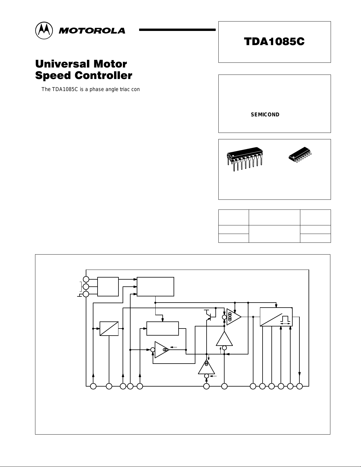
Figure 1. Representative Block Diagram and Pin Connections
+ V
CC
Shunt Regulator
Ballast Resistor
9
10
Voltage
8
Reg
Speed
Detector
12 11 4 5 6 3 7 16 14 15 2 1 13
Set Speed
Actual Speed
Digital Speed Sense
F/VC Pump Capacitor
MOTOROLA ANALOG IC DEVICE DATA
Monitoring
Ramp
Generator
Current
Ramp Current Gen. Control
Limiter
Reset
–
+
Control
Amp.
=
0.7 V
–V
CC
Motor Current Limit
Ramp Gen. Timing
Motorola, Inc. 1996 Rev 5
Trigger Pulse
Gen.
Sawtooth Capacitor
Closed Loop Stability
Sawtooth Set Current
Voltage Synchronization
Trigger Pulse Output
Current Synchronization
1

MAXIMUM RATINGS
Power Supply, when externally regulated, V
Maximum Voltage per listed pin
Pin 3
Pin 4–5–6–7–13–14–16
Pin 10
Maximum Current per listed pin
Pin 1 and 2
Pin 3
Pin 9 (VCC)
Pin 10 shunt regulator
Pin 12
Pin 13
Maximum Power Dissipation P
Thermal Resistance, Junction–to–Air R
Operating Junction Temperature T
Storage Temperature Range T
(TA = 25°C, voltages are referenced to Pin 8, ground)
Rating Symbol Value Unit
Pin 9
TDA1085C
V
CC
V
Pin
I
Pin
θJA
stg
– 3.0 to + 3.0
– 1.0 to + 1.0
D
– 10 to + 120 °C
J
– 55 to + 150 °C
15 V
+ 5.0
0 to + V
CC
0 to + 17
– 1.0 to + 0
15
35
– 200
1.0 W
65 °C/W
V
mA
ELECTRICAL CHARACTERISTICS (T
Characteristic
VOLTAGE REGULATOR
Internally Regulated Voltage (V
(I
= 0, I
Pin 7
VCC Temperature Factor TF — – 100 — ppm/°C
Current Consumption (I
(V9 = 15 V, V12 = V8 = 0, I1 = I2 = 100 µA,
all other pins not connected)
VCC Monitoring Enable Level
VCC Monitoring Disable Level
RAMP GENERATOR
Reference Speed Input Voltage Range V
Reference Input Bias Current – I
Ramp Selection Input Bias Current – I
Distribution Starting Level Range V
Distribution Final Level
V
= 0.75 V
Pin 6
High Acceleration Charging Current
V
= 0 V
Pin 7
V
= 10 V
Pin 7
Distribution Charging Current
V
= 2.0 V
Pin 7
Pin 9
+ I
Pin 10
Pin 9
Pin 9
= 15 mA, I
)
)
A
Pin 13
= 25°C)
= 0)
Symbol Min Typ Max Unit
V
CC
I
CC
VCC EN
VCC DIS
Pin 5
Pin 5
Pin 6
DS
VDF/V
DS
– I
Pin 7
– I
Pin 7
15 15.3 15.6 V
— 4.5 6.0 mA
—
—
0.08 — 13.5 V
0 0.8 1.0 µA
0 — 1.0 µA
0 — 2.0 V
2.0 2.09 2.2
1.0
1.0
4.0 5.0 6.0 µA
VCC– 0.4
VCC– 1.0
—
1.2
—
—
1.7
1.4
V
mA
2
MOTOROLA ANALOG IC DEVICE DATA
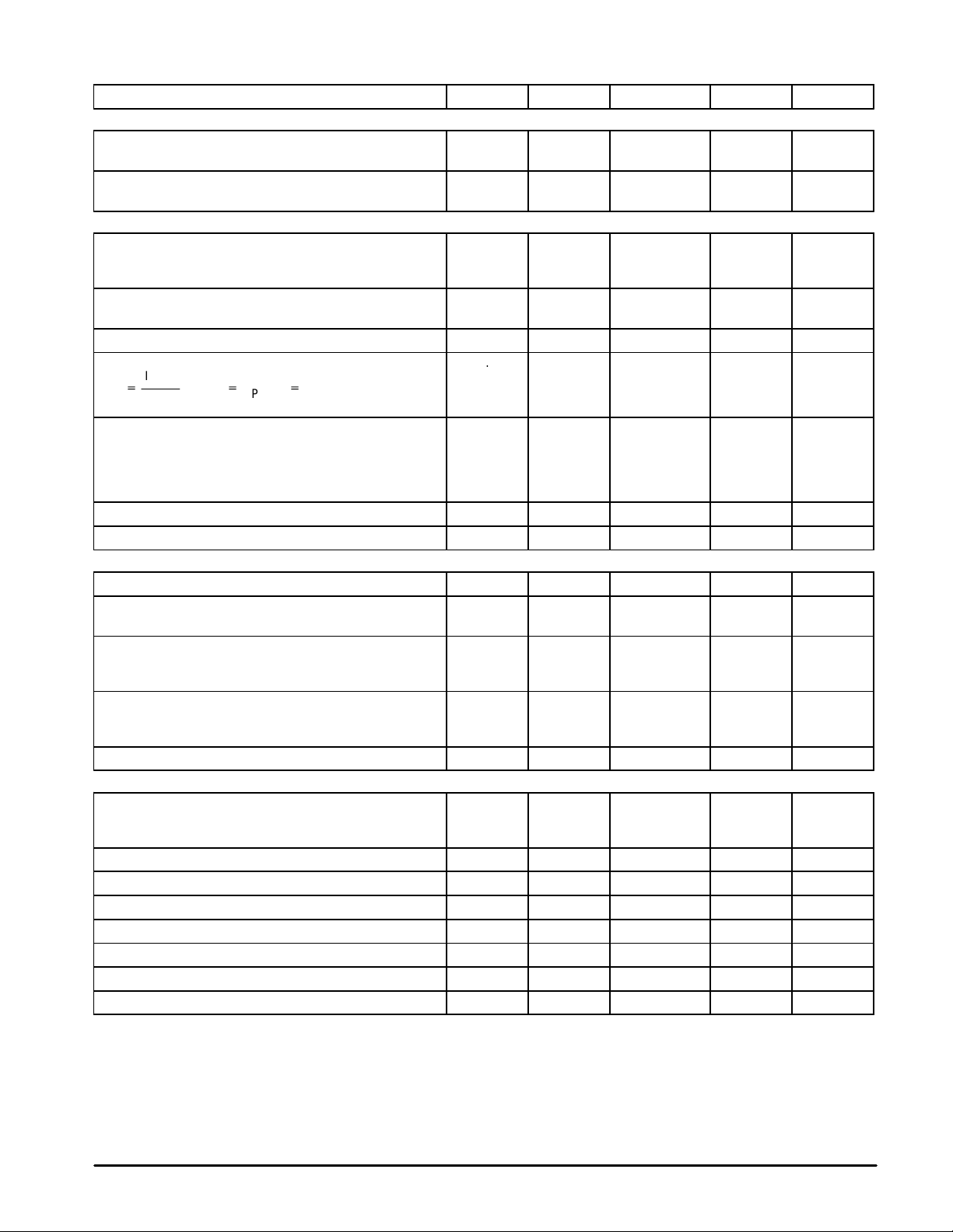
TDA1085C
ELECTRICAL CHARACTERISTICS (continued)
Characteristic Symbol Min Typ Max Unit
CURRENT LIMITER
Limiter Current Gain — I
(I
= – 300 µA)
Pin3
Detection Threshold Voltage
I
= – 10 µA
Pin 3
FREQUENCY TO VOLTAGE CONVERTER
Input Signal “Low Voltage”
Input Signal “High Voltage”
Monitoring Reset Voltage
Negative Clamping Voltage
I
= – 200 µA
Pin 12
Input Bias Current – I
Internal Current Source Gain
I
Pin4
G
+
Gain Linearity versus Voltage on Pin 4
(G
8.6
V4 = 0 V
V4 = 4.3 V
V4 = 12 V
Gain Temperature Effect (V
Output Leakage Current (I
CONTROL AMPLIFIER
Actual Speed Input Voltage Range V
Input Offset Voltage V
(I
Pin 16
Amplifier Transconductance
(I
Pin 16
(I
Pin 16
Output Current Swing Capability
Source
Sink
Output Saturation Voltage V16
TRIGGER PULSE GENERATOR
Synchronization Level Currents
Voltage Line Sensing
Triac Sensing
Trigger Pulse Duration (C
Trigger Pulse Repetition Period, conditions as a.m. T
Output Pulse Current V
Output Leakage Current V
Full Angle Conduction Input Voltage V
Saw Tooth “High” Level Voltage V14
Saw Tooth Discharge Current, I
,V
I
Pin11
= Gain for V
= 0, V
/∆ (V5 – V4)
= + and – 50 µA, V
Pin 7/IPin 3
+
Pin4
Pin 4
Pin 5
= 3.0 and 8.0 V)
Pin 16
Pin 13
V
Pin 3 TH
V12
V12
– V12
V
+
Pin11
= 8.6 V)
Pin 4
Pin 11
– V
Pin 14
Pin 13
0
G/G
= 0) TF — 350 — ppm/°C
= 0) – I
Pin 4
= 3.0 V)
Pin 16
I
= 47 nF, R
= VCC – 4.0 V – I
= – 3.0 V I13
= 100 µA I
Pin15
= 270 kΩ) T
Pin 15
C
g
V12
L
H
R
CL
Pin12
G.0 9.5 — 11
8.6
Pin 4
Pin 4
V
off
T 270 340 400 µA/V
Pin 16
sat
I
Pin 2
I
Pin 1
p
R
Pin 13
L
14
H
Pin 14
130 180 250
50 65 80 mV
–100
+100
5.0
— 0.6 — V
— 25 — µA
1.04
1.015
0.965
0 — 100 nA
0 — 13.5 V
0 — 50 mV
– 200
50
— — 0.8 V
—
—
— 55 — µs
— 220 — µs
180 192 — mA
— — 30 µA
— 11.7 — V
12 — 12.7 V
95 — 105 µA
—
—
—
1.05
1.025
0.975
– 100
100
± 50
± 50
—
—
—
1.06
1.035
0.985
– 50
200
± 100
± 100
mV
mV
V
µA
µA
MOTOROLA ANALOG IC DEVICE DATA
3

TDA1085C
GENERAL DESCRIPTION
The TDA 1085C triggers a triac accordingly to the speed regulation
requirements. Motor speed is digitally sensed by a tachogenerator
and then converted into an analog voltage.
The speed set is externally fixed and is applied to the internal linear
regulation input after having been submitted to programmable
acceleration ramps. The overall result consists in a full motor speed
INPUT/OUTPUT FUNCTIONS
(Refer to Figures 1 and 8)
Voltage Regulator – (Pins 9 and 10) This is a parallel type regulator
able to sink a large amount of current and offering good
characteristics. Current flow is provided from AC line by external
dropping resistors R1, R2, and rectifier: This half wave current is
used to feed a smoothering capacitor, the voltage of which is
checked by the IC.
When VCC is reached, the excess of current is derived by another
dropping resistor R10 and by Pin 10. These three resistors must be
determined in order:
• T o let 1.0 mA flow through Pin 10 when AC line is minimum and V
consumption is maximum (fast ramps and pulses present).
• T o let V
VCC consumption is minimum (no ramps and no pulses).
reach 3.0 V when AC line provides maximum current and
10
CC
• All along the main line cycle, the Pin 10 dynamic range must not be
exceeded unless loss of regulation.
An AC line supply failure would cause shut down.
The double capacitive filter built with R1 and R2 gives an efficient
VCC smoothing and helps to remove noise from set speeds.
Speed Sensing – (Pins 4, 11, 12) The IC is compatible with an
external analog speed sensing: its output must be applied to Pin 4,
and Pin 12 connected to Pin 8.
In most of the applications it is more convenient to use a digital
speed sensing with an unexpensive tachogenerator which
doesn′t need any tuning. During every positive cycle at Pin 12,
the capacitor C
time, Pin 4 delivers a current which is 10 times the one charging
C
specified, but nevertheless requires an adjustment on R
current into this resistor is proportional to C
speed; being filtered by a capacitor, V
and represents the “true actual motor speed”.
T o maintain linearity into the high speed range, it is important to verify
that C
impedance. Nevertheless C
has a large influence on FV/C temperature factor. A 470 KΩ resistor
between Pins 11 and 9 reduces leakage currents and temperature
factor as well, down to neglectable effects.
Pin 12 also has a monitoring function: when its voltage is above
5.0 V, the trigger pulses are inhibited and the IC is reset. It also
senses the tachogenerator continuity, and in case of any circuit
aperture, it inhibits pulse, avoiding the motor to run out of control. In
the TDA 1085C, Pin 12 is negatively clamped by an internal diode
which removes the necessity of the external one used in the former
circuit.
. The current source gain is called G and is tightly
Pin 11
is fully charged: the internal source on Pin 11 has 100KΩ
Pin 11
is charged to almost VCC and during this
Pin 11
and to the motor
Pin 11
becomes smothered
Pin 4
has to be as high as possible as it
Pin 11
Pin 4
. The
range with two acceleration ramps which allow efficient washing
machine control (Distribute function).
Additionally, the TDA 1085C protects the whole system against AC
line stop or variations, overcurrent in the motor and tachogenerator
failure.
Ramp Generator – (Pins 5, 6, 7) The true Set Speed value taken in
consideration by the regulation is the output of the ramp generator
(Pin 7). With a given value of speed set input (Pin 5), the ramp
generator charges an external capacitor C
V
(set speed) equals V
Pin 5
has an internal charging current source of 1.2mA and delivers it from
0 to 12 V at Pin 7. It is the high acceleration ramp (5.0 s typical) which
allows rapid motor speed changes without excessive strains on the
mechanics. In addition, the TDA 1085C offers the possibility to break
this high acceleration with the introduction of a low acceleration ramp
(called Distribution) by reducing the Pin 7 source current down to
5.0 µA under Pin 6 full control, as shown by following conditions:
(true speed), see Figure 2. The IC
Pin 4
• Presence of high acceleration ramp V
• Distribution occurs in the V
by V
For two fixed values of V
high acceleration, excluding the time for V
to two times this value, high acceleration again, up to the moment
the motor has reached the set speed value, at which it will stay,
see Figure 3.
Should a reset happen (whatever the cause would be), the above
mentioned successive ramps will be fully reprocessed from 0 to the
maximum speed. If V
occurs.
To get a real zero speed position, Pin 5 has been designed in such a
way that its voltage from 0 to 80 mV is interpreted as a true zero. As
a consequence, when changing the speed set position, the designer
must be sure that any transient zero would not occur: if any, the entire
circuit will be reset.
As the voltages applied by Pins 5 and 6 are derived from the internal
voltage regulator supply and Pin 4 voltage is also derived from the
same source, motor speed (which is determined by the ratios
between above mentioned voltages) is totally independent from V
variations and temperature factor.
Control Amplifier – (Pin 16) It amplifies the difference between true
speed (Pin 4) and set speed (Pin 5), through the ramp generator. Its
output available at Pin 16 is a double sense current source with a
maximum capability of ± 100 µA and a specified transconductance
(340 µA/V typical). Pin 16 drives directly the trigger pulse generator,
and must be loaded by an electrical network which compensates the
mechanical characteristics of the motor and its load, in order to
provide stability in any condition and shortest transient response; see
Figure 4.
This network must be adjusted experimentally.
In case of a periodic torque variations, Pin 16 directly provides the
phase angle oscillations.
Pin 6
x V
Pin 4
x 2.0 V
Pin 5
Pin 6
range (true motor speed) defined
Pin 4
Pin 6
and V
Pin 6
= 0, only the high acceleration ramp
up to the moment
Pin 7
> V
Pin 5
, the motor speed will have
Pin 4
to go from V
Pin 4
Pin 6
CC
4
MOTOROLA ANALOG IC DEVICE DATA
 Loading...