

Motorola MC74HC173AD Datasheet
SEMICONDUCTOR TECHNICAL DATA
1
REV 0
Motorola, Inc. 1997
6/97
! "
High–Performance Silicon–Gate CMOS
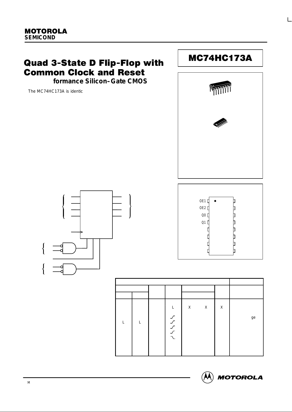
The MC74HC173A is identical in pinout to the LS173. The device inputs
are compatible with standard CMOS outputs; with pullup resistors, they are
compatible with LSTTL outputs.
Data, when enabled, are clocked into the four D flip–flops with the rising
edge of the common Clock. When either or both of the Output Enable
Controls is high, the outputs are in a high–impedance state. This feature
allows the HC173A to be used in bus–oriented systems. The Reset feature
is asynchronous and active high.
• Output Drive Capability: 15 LSTTL Loads
• Outputs Directly Interface to CMOS, NMOS, and TTL
• Operating Voltage Range: 2 to 6 V
• Low Input Current: 1 µA
• High Noise Immunity Characteristic of CMOS Devices
• In Compliance with the Requirements Defined by JEDEC Standard
No. 7A
• Chip Complexity 208 FETs or 52 Equivalent Gates
FUNCTION TABLE
Inputs Output
Output Enables
Data Enables
Data
OE1 OE2
Reset Clock
DE1 DE2
Data
D
Q
L L H X X X X L
L L L L X XXNo Change
L L L H X XXNo Change
L L L H XXNo Change
L L L X HXNo Change
L L L L LL L
L L L L LH H
L L L X XXNo Change
L H X X X XXHigh Impedance
H L X X X XXHigh Impedance
H H X X X X X High Impedance
PIN ASSIGNMENT
13
14
15
16
9
10
11
125
4
3
2
1
8
7
6
D2
D1
D0
RESET
V
CC
DE1
DE2
D3
Q1
Q0
OE2
OE1
GND
CLOCK
Q3
Q2
D SUFFIX
16–LEAD PLASTIC SOIC PACKAGE
CASE 751B–05
N SUFFIX
16–LEAD PLASTIC DIP PACKAGE
CASE 648–08
ORDERING INFORMATION
MC74HCXXXAN
MC74HCXXXAD
Plastic
SOIC
LOGIC DIAGRAM
VCC = PIN 16
GND = PIN 8
DATA
INPUTS
3–STATE
NONINVERTING
OUTPUTS
D0
D1
D2
D3
14
13
12
11
3
4
5
6
Q0
Q1
Q2
Q3
CLOCK
7
DATA–
ENABLES
OUTPUT
ENABLES
DE1
DE2
OE1
OE2
RESET
9
10
15
1
2
MC74HC173A
MOTOROLA High–Speed CMOS Logic Data
DL129 — Rev 6
2
MAXIMUM RATINGS*
Symbol
Parameter
Value
Unit
V
CC
DC Supply Voltage (Referenced to GND)
– 0.5 to + 7.0
V
V
in
DC Input Voltage (Referenced to GND)
– 0.5 to VCC + 0.5
V
V
out
DC Output Voltage (Referenced to GND)
– 0.5 to VCC + 0.5
V
I
in
DC Input Current, per Pin
± 20
mA
I
out
DC Output Current, per Pin
± 35
mA
I
CC
DC Supply Current, VCC and GND Pins
± 75
mA
P
D
Power Dissipation in Still Air Plastic DIP†
SOIC Package†
750
500
mW
T
stg
Storage Temperature
– 65 to + 150
_
C
Î
Î
T
L
ОООООООООООО
Î
Lead Temperature, 1 mm from Case for 10 Seconds
(Plastic DIP or SOIC Package)
ÎÎÎÎ
Î
260
Î
Î
_
C
*Maximum Ratings are those values beyond which damage to the device may occur .
Functional operation should be restricted to the Recommended Operating Conditions.
†Derating — Plastic DIP: – 10 mW/_C from 65_ to 125_C
SOIC Package: – 7 mW/_C from 65_ to 125_C
For high frequency or heavy load considerations, see Chapter 2 of the Motorola High–Speed CMOS Data Book (DL129/D).
RECOMMENDED OPERATING CONDITIONS
Symbol
Parameter
Min
Max
Unit
ÎÎ
V
CC
ОООООООООООО
DC Supply Voltage (Referenced to GND)
Î
2.0Î6.0ÎV
Vin, V
out
DC Input Voltage, Output Voltage (Referenced to GND)
0
V
CC
V
T
A
Operating Temperature, All Package Types
– 55
+ 125
_
C
ÎÎ
Î
ÎÎ
Î
tr, t
f
ОООООООООООО
Î
ОООООООООООО
Î
Input Rise and Fall Time VCC = 2.0 V
(Figure 1) VCC = 4.5 V
VCC = 6.0 V
Î
Î
Î
Î
0
0
0
Î
Î
Î
Î
1000
500
400
Î
Î
Î
Î
ns
DC ELECTRICAL CHARACTERISTICS (Voltages Referenced to GND)
Guaranteed Limit
ÎÎ
Î
Symbol
ООООООО
Î
Parameter
ООООООО
Î
Test Conditions
ÎÎ
Î
V
CC
V
ÎÎ
– 55 to
25_C
ÎÎ
Î
v
85_C
ÎÎ
Î
v
125_C
Î
Î
Unit
ÎÎ
Î
ÎÎ
Î
V
IH
ООООООО
Î
ООООООО
Î
Minimum High–Level Input
Voltage
ООООООО
Î
ООООООО
Î
V
out
= 0.1 V or VCC – 0.1 V
|I
out
| v 20 µA
ÎÎ
Î
ÎÎ
Î
2.0
3.0
4.5
6.0
ÎÎ
ÎÎ
1.5
2.1
3.15
4.2
ÎÎ
Î
ÎÎ
Î
1.5
2.1
3.15
4.2
ÎÎ
Î
ÎÎ
Î
1.5
2.1
3.15
4.2
Î
Î
Î
Î
V
ÎÎ
Î
ÎÎ
Î
V
IL
ООООООО
Î
ООООООО
Î
Maximum Low–Level Input
Voltage
ООООООО
Î
ООООООО
Î
V
out
= 0.1 V or VCC – 0.1 V
|I
out
| v 20 µA
ÎÎ
Î
ÎÎ
Î
2.0
3.0
4.5
6.0
ÎÎ
ÎÎ
0.5
0.9
1.35
1.8
ÎÎ
Î
ÎÎ
Î
0.5
0.9
1.35
1.8
ÎÎ
Î
ÎÎ
Î
0.5
0.9
1.35
1.8
Î
Î
Î
Î
V
ÎÎ
Î
V
OH
ООООООО
Î
Minimum High–Level Output
Voltage
ООООООО
Î
Vin = VIH or V
IL
|I
out
| v 20 µA
ÎÎ
Î
2.0
4.5
6.0
ÎÎ
1.9
4.4
5.9
ÎÎ
Î
1.9
4.4
5.9
ÎÎ
Î
1.9
4.4
5.9
Î
Î
V
ÎÎ
Î
ÎÎ
Î
ООООООО
Î
ООООООО
Î
ООООООО
Î
ООООООО
Î
Vin = VIH or VIL|I
out
| v 3.6 mA
|I
out
| v 6.0 mA
|I
out
| v 7.8 mA
ÎÎ
Î
ÎÎ
Î
3.0
4.5
6.0
ÎÎ
ÎÎ
2.48
3.98
5.48
ÎÎ
Î
ÎÎ
Î
2.34
3.84
5.34
ÎÎ
Î
ÎÎ
Î
2.20
3.70
5.20
Î
Î
Î
Î
ÎÎ
Î
ÎÎ
Î
V
OL
ООООООО
Î
ООООООО
Î
Maximum Low–Level Output
Voltage
ООООООО
Î
ООООООО
Î
Vin = VIH or V
IL
|I
out
| v 20 µA
ÎÎ
Î
ÎÎ
Î
2.0
4.5
6.0
ÎÎ
ÎÎ
0.1
0.1
0.1
ÎÎ
Î
ÎÎ
Î
0.1
0.1
0.1
ÎÎ
Î
ÎÎ
Î
0.1
0.1
0.1
Î
Î
Î
Î
V
ÎÎÎОООООООÎООООООО
Î
Vin = VIH or VIL|I
out
| v 3.6 mA
|I
out
| v 6.0 mA
|I
out
| v 7.8 mA
ÎÎ
Î
3.0
4.5
6.0
ÎÎ
0.26
0.26
0.26
ÎÎ
Î
0.33
0.33
0.33
ÎÎ
Î
0.40
0.40
0.40
Î
Î
This device contains protection
circuitry to guard against damage
due to high static voltages or electric
fields. However, precautions must
be taken to avoid applications of any
voltage higher than maximum rated
voltages to this high–impedance circuit. For proper operation, Vin and
V
out
should be constrained to the
range GND v (Vin or V
out
) v VCC.
Unused inputs must always be
tied to an appropriate logic voltage
level (e.g., either GND or VCC).
Unused outputs must be left open.
MC74HC173A
High–Speed CMOS Logic Data
DL129 — Rev 6
3 MOTOROLA
DC ELECTRICAL CHARACTERISTICS (Voltages Referenced to GND)
Unit
Guaranteed Limit
V
CC
V
Test Conditions
Parameter
Symbol
Unit
v
125_C
v
85_C
– 55 to
25_C
V
CC
V
Test Conditions
Parameter
Symbol
I
in
Maximum Input Leakage Current
Vin = VCC or GND
6.0
± 0.1
± 1.0
± 1.0
µA
ÎÎ
Î
ÎÎ
Î
I
OZ
ООООООО
Î
ООООООО
Î
Maximum Three–State
Leakage Current
ООООООО
Î
ООООООО
Î
Output in High–Impedance State
Vin = VIL or V
IH
V
out
= VCC or GND
ÎÎ
Î
ÎÎ
Î
6.0
ÎÎ
ÎÎ
± 0.5
ÎÎ
Î
ÎÎ
Î
± 5.0
ÎÎ
Î
ÎÎ
Î
± 10
Î
Î
Î
Î
µA
I
CC
Maximum Quiescent Supply
Current (per Package)
Vin = VCC or GND
I
out
= 0 µA
6.0
4
40
160
µA
NOTE:Information on typical parametric values can be found in Chapter 2 of the Motorola High–Speed CMOS Data Book (DL129/D).
AC ELECTRICAL CHARACTERISTICS (C
L
= 50 pF, Input tr = tf = 6 ns)
Guaranteed Limit
ÎÎ
Î
Symbol
ООООООООООООООО
Î
Parameter
ÎÎ
Î
V
CC
V
ÎÎ
– 55 to
25_C
ÎÎ
Î
v
85_C
ÎÎ
Î
v
125_C
Î
Î
Unit
ÎÎ
Î
ÎÎ
Î
f
max
ООООООООООООООО
Î
ООООООООООООООО
Î
Maximum Clock Frequency (50% Duty Cycle)
(Figures 1 and 5)
ÎÎ
Î
ÎÎ
Î
2.0
3.0
4.5
6.0
ÎÎ
ÎÎ
6.0
10
30
35
ÎÎ
Î
ÎÎ
Î
4.8
8.0
24
28
ÎÎ
Î
ÎÎ
Î
4.0
6.0
20
24
Î
Î
Î
Î
MHz
ÎÎ
Î
ÎÎ
Î
t
PLH
,
t
PHL
ООООООООООООООО
Î
ООООООООООООООО
Î
Maximum Propagation Delay, Clock to Q
(Figures 1 and 5)
ÎÎ
Î
ÎÎ
Î
2.0
3.0
4.5
6.0
ÎÎ
ÎÎ
175
150
35
30
ÎÎ
Î
ÎÎ
Î
220
175
44
37
ÎÎ
Î
ÎÎ
Î
265
220
53
45
Î
Î
Î
Î
ns
ÎÎ
Î
ÎÎ
Î
t
PHL
ООООООООООООООО
Î
ООООООООООООООО
Î
Maximum Propagation Delay, Reset to Q
(Figures 2 and 5)
ÎÎ
Î
ÎÎ
Î
2.0
3.0
4.5
6.0
ÎÎ
ÎÎ
150
125
30
26
ÎÎ
Î
ÎÎ
Î
190
150
38
33
ÎÎ
Î
ÎÎ
Î
225
175
45
38
Î
Î
Î
Î
ns
ÎÎ
Î
ÎÎ
t
PLZ
,
t
PHZ
ООООООООООООООО
Î
ООООООООООООООО
Maximum Propagation Delay, Output Enable to Q
(Figures 3 and 6)
ÎÎ
Î
ÎÎ
2.0
3.0
4.5
6.0
ÎÎ
ÎÎ
150
125
30
26
ÎÎ
Î
ÎÎ
190
150
38
33
ÎÎ
Î
ÎÎ
225
175
45
38
Î
Î
Î
ns
ÎÎ
Î
ÎÎ
Î
t
PZL
,
t
PZH
ООООООООООООООО
Î
ООООООООООООООО
Î
Maximum Propagation Delay, Output Enable to Q
(Figures 3 and 6)
ÎÎ
Î
ÎÎ
Î
2.0
3.0
4.5
6.0
ÎÎ
ÎÎ
150
125
30
26
ÎÎ
Î
ÎÎ
Î
190
150
38
33
ÎÎ
Î
ÎÎ
Î
225
175
45
38
Î
Î
Î
Î
ns
ÎÎ
Î
ÎÎ
Î
t
TLH
,
t
THL
ООООООООООООООО
Î
ООООООООООООООО
Î
Maximum Output Transition Time, Any Output
(Figures 1 and 5)
ÎÎ
Î
ÎÎ
Î
2.0
3.0
4.5
6.0
ÎÎ
ÎÎ
60
22
12
10
ÎÎ
Î
ÎÎ
Î
75
28
15
13
ÎÎ
Î
ÎÎ
Î
90
34
18
15
Î
Î
Î
Î
ns
C
in
Maximum Input Capacitance
—
10
10
10
pF
ÎÎ
Î
C
out
ООООООООООООООО
Î
Maximum Three–State Output Capacitance
(Output in High–Impedance State)
ÎÎ
Î
—
ÎÎ15ÎÎ
Î
15
ÎÎ
Î
15
Î
Î
pF
NOTES:
1. For propagation delays with loads other than 50 pF, see Chapter 2 of the Motorola High–Speed CMOS Data Book (DL129/D).
2. Information on typical parametric values can be found in Chapter 2 of the Motorola High–Speed CMOS Data Book (DL129/D).
Typical @ 25°C, VCC = 5.0 V
C
PD
Power Dissipation Capacitance (Per Flip–Flop)*
35
pF
*Used to determine the no–load dynamic power consumption: PD = CPD V
CC
2
f + ICC VCC. For load considerations, see Chapter 2 of the
Motorola High–Speed CMOS Data Book (DL129/D).
 Loading...