

SEMICONDUCTOR TECHNICAL DATA
" #"
#"#" " !"
High–Performance Silicon–Gate CMOS
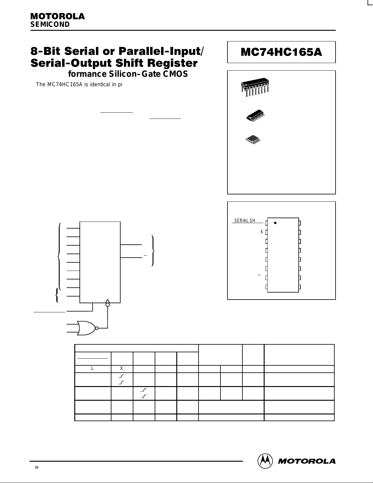
The MC74HC165A is identical in pinout to the LS165. The device inputs
are compatible with standard CMOS outputs; with pullup resistors, they are
compatible with LSTTL outputs.
This device is an 8–bit shift register with complementary outputs from the
last stage. Data may be loaded into the register either in parallel or in serial
form. When the Serial Shift/Parallel Load
asynchronously in parallel. When the Serial Shift/Parallel Load
the data is loaded serially on the rising edge of either Clock or Clock Inhibit
(see the Function Table).
The 2–input NOR clock may be used either by combining two independent
clock sources or by designating one of the clock inputs to act as a clock
inhibit.
• Output Drive Capability: 10 LSTTL Loads
• Outputs Directly Interface to CMOS, NMOS, and TTL
• Operating Voltage Range: 2 to 6 V
• Low Input Current: 1 µA
• High Noise Immunity Characteristic of CMOS Devices
• In Compliance with the Requirements Defined by JEDEC Standard
No. 7A
• Chip Complexity: 286 FETs or 71.5 Equivalent Gates
LOGIC DIAGRAM
11
A
12
B
13
PARALLEL
DATA
INPUTS
SERIAL
DATA
INPUT
SERIAL SHIFT/
PARALLEL LOAD
CLOCK INHIBIT
C
D
E
F
G
H
S
A
CLOCK
14
3
4
5
6
10
1
2
15
Serial Shift/
Parallel Load
L X X X a … h a b h Asynchronous Parallel Load
H
H
H
H
H
H
H L L X X No Change No Clock
X = don’t care QAn – QGn = Data shifted from the preceding stage
input is low, the data is loaded
input is high,
9
Q
SERIAL
H
7
DATA
OUTPUTS
Q
H
PIN 16 = V
PIN 8 = GND
CC
FUNCTION TABLE
Inputs Internal Stages Output
Clock
Clock
Inhibit
L
L
L
L
X
H
H
X
S
A
L
H
L
H
X
X
A – H Q
X
X
X
X
X
X
H
H
16
1
16
1
16
1
ORDERING INFORMATION
MC74HCXXXAN
MC74HCXXXAD
MC74HCXXXADT
PIN ASSIGNMENT
SERIAL SHIFT/
PARALLEL LOAD
CLOCK
Q
A
L
L
Q
An
Q
An
Q
An
Q
An
No Change Inhibited Clock
Q
B
Q
Gn
Q
Gn
Q
Gn
Q
Gn
1
2
E
3
F
4
G
6
H
7
Q
H
8
GND
H
Serial Shift via Clock
Serial Shift via Clock Inhibit
N SUFFIX
PLASTIC PACKAGE
CASE 648–08
D SUFFIX
SOIC PACKAGE
CASE 751B–05
DT SUFFIX
TSSOP PACKAGE
CASE 948F–01
Plastic
SOIC
TSSOP
V
16
CC
CLOCK INHIBIT
15
D
14
C
13
B
125
A
11
S
10
A
Q
9
H
Operation
This document contains information on a product under development. Motorola reserves the right to change or
discontinue this product without notice.
3/98
Motorola, Inc. 1998
1
REV 1
MC74HC165A
Î
Î
Î
Î
Î
Î
Î
Î
Î
Î
Î
Î
Î
Î
Î
Î
Î
Î
Î
Î
Î
Î
Î
Î
Î
Î
Î
Î
Î
Î
Î
Î
Î
Î
Î
Î
Î
Î
Î
Î
Î
Î
Î
Î
Î
Î
Î
Î
Î
Î
Î
Î
Î
Î
Î
Î
Î
Î
Î
Î
Î
Î
Î
Î
Î
MAXIMUM RATINGS*
Symbol
V
V
I
I
Î
Î
T
Î
Î
DC Supply Voltage (Referenced to GND)
CC
V
DC Input Voltage (Referenced to GND)
in
DC Output Voltage (Referenced to GND)
out
I
DC Input Current, per Pin
in
DC Output Current, per Pin
out
DC Supply Current, VCC and GND Pins
CC
P
Power Dissipation in Still Air Plastic DIP†
D
ОООООООООООО
ОООООООООООО
Storage Temperature
stg
ОООООООООООО
T
Lead Temperature, 1 mm from Case for 10 Seconds
L
ОООООООООООО
*Maximum Ratings are those values beyond which damage to the device may occur.
Functional operation should be restricted to the Recommended Operating Conditions.
†Derating — Plastic DIP: – 10 mW/_C from 65_ to 125_C
SOIC Package: – 7 mW/_C from 65_ to 125_C
TSSOP Package: – 6.1 mW/_C from 65_ to 125_C
For high frequency or heavy load considerations, see Chapter 2 of the Motorola High–Speed CMOS Data Book (DL129/D).
Parameter
SOIC Package†
TSSOP Package†
(Plastic DIP, SOIC or TSSOP Package)
Value
– 0.5 to + 7.0
– 0.5 to VCC + 0.5
– 0.5 to VCC + 0.5
± 20
± 25
± 50
750
500
ÎÎÎÎ
450
ÎÎÎÎ
– 65 to + 150
ÎÎÎÎ
ÎÎÎÎ
260
Unit
V
V
V
mA
mA
mA
mW
Î
Î
_
C
Î
_
C
Î
This device contains protection
circuitry to guard against damage
due to high static voltages or electric
fields. However, precautions must
be taken to avoid applications of any
voltage higher than maximum rated
voltages to this high–impedance circuit. For proper operation, Vin and
V
should be constrained to the
out
range GND v (Vin or V
Unused inputs must always be
tied to an appropriate logic voltage
level (e.g., either GND or VCC).
Unused outputs must be left open.
) v VCC.
out
RECOMMENDED OPERATING CONDITIONS
Symbol
V
CC
Vin, V
T
A
tr, t
ÎÎ
ÎÎ
DC Supply Voltage (Referenced to GND)
DC Input Voltage, Output Voltage (Referenced to GND)
out
Operating Temperature, All Package Types
Input Rise and Fall Time VCC = 2.0 V
f
(Figure 1) VCC = 3.0 V
ОООООООООООО
ОООООООООООО
Parameter
VCC = 4.5 V
VCC = 6.0 V
Min
2.0
0
– 55
0
0
Î
0
Î
DC ELECTRICAL CHARACTERISTICS (Voltages Referenced to GND)
ÎÎ
Symbol
V
IH
ÎÎ
ÎÎ
V
IL
ÎÎ
ÎÎ
V
OH
ÎÎ
ÎÎÎОООООООÎООООООО
ООООООО
Parameter
Minimum High–Level Input
Voltage
ООООООО
ООООООО
Maximum Low–Level Input
Voltage
ООООООО
ООООООО
Minimum High–Level Output
Voltage
ООООООО
ООООООО
Test Conditions
V
= 0.1 V or VCC – 0.1 V
out
|I
| v 20 µA
ООООООО
out
ООООООО
V
= 0.1 V or VCC – 0.1 V
out
|I
| v 20 µA
out
ООООООО
ООООООО
Vin = VIH or V
|I
| v 20 µA
out
ООООООО
Vin = VIH or VIL|I
IL
| v 2.4 mA
out
|I
| v 4.0 mA
out
|I
| v 5.2 mA
out
Max
6.0
V
CC
+ 125
1000
600
Î
500
400
Î
Unit
V
V
_
C
ns
Î
Î
V
CC
ÎÎ
V
2.0
3.0
ÎÎ
4.5
ÎÎ
6.0
2.0
3.0
ÎÎ
4.5
ÎÎ
6.0
2.0
4.5
ÎÎ
6.0
3.0
4.5
ÎÎ
6.0
Guaranteed Limit
– 55 to
ÎÎ
25_C
ÎÎ
1.5
2.1
ÎÎ
ÎÎ
3.15
4.2
ÎÎ
ÎÎ
0.5
0.9
ÎÎ
ÎÎ
1.35
1.80
ÎÎ
ÎÎ
1.9
4.4
ÎÎ
5.9
ÎÎ
2.48
3.98
ÎÎ
ÎÎ
5.48
v
85_C
1.5
2.1
3.15
4.2
0.5
0.9
1.35
1.80
1.9
4.4
5.9
2.34
3.84
5.34
ÎÎ
v
125_C
1.5
2.1
ÎÎ
3.15
ÎÎ
4.2
0.5
0.9
ÎÎ
1.35
ÎÎ
1.80
1.9
4.4
ÎÎ
5.9
2.20
3.70
ÎÎ
5.20
Î
Unit
Î
Î
Î
Î
Î
Î
V
V
V
V
MOTOROLA High–Speed CMOS Logic Data
2
DL129 — Rev 6
MC74HC165A
Î
Î
Î
Î
Î
Î
Î
Î
Î
Î
Î
Î
Î
Î
Î
Î
Î
Î
Î
Î
Î
Î
Î
Î
Î
Î
Î
Î
Î
Î
Î
Î
Î
Î
Î
Î
Î
Î
Î
Î
Î
Î
Î
Î
Î
Î
Î
Î
Î
Î
Î
Î
Î
Î
Î
Î
Î
Î
Î
Î
Î
Î
Î
Î
Î
Î
Î
Î
Î
Î
Î
Î
Î
Î
Î
Î
Î
Î
Î
Î
Î
Î
Î
Î
Î
DC ELECTRICAL CHARACTERISTICS (Voltages Referenced to GND)
Guaranteed Limit
V
V
Symbol
Symbol
V
OL
ÎÎ
ÎÎÎОООООООÎООООООО
I
in
I
CC
ÎÎ
Maximum Low–Level Output
Voltage
ООООООО
Maximum Input Leakage Current
Maximum Quiescent Supply
ООООООО
Current (per Package)
Parameter
Parameter
Test Conditions
Test Conditions
Vin = VIH or V
|I
| v 20 µA
out
ООООООО
Vin = VIH or VIL|I
IL
| v 2.4 mA
out
|I
| v 4.0 mA
out
|I
| v 5.2 mA
out
Vin = VCC or GND
Vin = VCC or GND
ООООООО
I
= 0 µA
out
2.0
4.5
ÎÎ
6.0
3.0
4.5
ÎÎ
6.0
6.0
6.0
ÎÎ
NOTE:Information on typical parametric values can be found in Chapter 2 of the Motorola High–Speed CMOS Data Book (DL129/D).
CC
CC
V
V
– 55 to
25_C
v
0.1
0.1
ÎÎ
0.1
ÎÎ
0.26
0.26
ÎÎ
± 0.1
ÎÎ4ÎÎ
0.26
ÎÎ
± 1.0
85_C
0.1
0.1
0.1
0.33
0.33
0.33
40
v
125_C
0.1
0.1
ÎÎ
0.1
0.40
0.40
ÎÎ
0.40
± 1.0
160
ÎÎ
Unit
Unit
Î
Î
µA
µA
Î
V
AC ELECTRICAL CHARACTERISTICS (C
= 50 pF, Input tr = tf = 6 ns)
L
Guaranteed Limit
ÎÎ
Symbol
f
max
ÎÎ
ÎÎ
t
,
PLH
t
PHL
ÎÎ
ÎÎ
t
,
PLH
t
PHL
ÎÎ
ÎÎ
t
,
PLH
t
PHL
ÎÎ
ÎÎ
t
,
TLH
t
THL
ÎÎ
ÎÎ
C
in
ООООООООООООООО
Parameter
Maximum Clock Frequency (50% Duty Cycle)
(Figures 1 and 8)
ООООООООООООООО
ООООООООООООООО
Maximum Propagation Delay, Clock (or Clock Inhibit) to QH or Q
(Figures 1 and 8)
ООООООООООООООО
ООООООООООООООО
Maximum Propagation Delay, Serial Shift/Parallel Load to QH or Q
(Figures 2 and 8)
ООООООООООООООО
ООООООООООООООО
Maximum Propagation Delay, Input H to QH or Q
(Figures 3 and 8)
ООООООООООООООО
ООООООООООООООО
H
Maximum Output Transition Time, Any Output
(Figures 1 and 8)
ООООООООООООООО
ООООООООООООООО
Maximum Input Capacitance
H
H
V
CC
ÎÎ
2.0
3.0
ÎÎ
4.5
ÎÎ
6.0
2.0
3.0
ÎÎ
4.5
ÎÎ
6.0
2.0
3.0
ÎÎ
4.5
ÎÎ
6.0
2.0
3.0
ÎÎ
4.5
6.0
ÎÎ
2.0
3.0
ÎÎ
4.5
6.0
ÎÎ
—
– 55 to
V
ÎÎ
25_C
ÎÎ
ÎÎ
ÎÎ
ÎÎ
ÎÎ
ÎÎ
ÎÎ
ÎÎ
ÎÎ
ÎÎ
6
18
30
35
150
52
30
26
175
58
35
30
150
52
30
26
75
27
15
13
10
ÎÎ
v
85_C
4.8
17
ÎÎ
24
ÎÎ
28
190
63
ÎÎ
38
ÎÎ
33
220
70
ÎÎ
44
ÎÎ
37
190
63
ÎÎ
38
33
ÎÎ
95
32
ÎÎ
19
16
ÎÎ
10
ÎÎ
v
125_C
ÎÎ
ÎÎ
ÎÎ
ÎÎ
ÎÎ
ÎÎ
ÎÎ
ÎÎ
ÎÎ
ÎÎ
NOTES:
1. For propagation delays with loads other than 50 pF, see Chapter 2 of the Motorola High–Speed CMOS Data Book (DL129/D).
2. Information on typical parametric values can be found in Chapter 2 of the Motorola High–Speed CMOS Data Book (DL129/D).
4
15
20
24
225
65
45
38
265
72
53
45
225
65
45
38
110
36
22
19
10
Î
Unit
MHz
Î
Î
Î
Î
Î
Î
Î
Î
Î
Î
pF
ns
ns
ns
ns
C
PD
Power Dissipation Capacitance (Per Package)*
*Used to determine the no–load dynamic power consumption: PD = CPD V
Motorola High–Speed CMOS Data Book (DL129/D).
High–Speed CMOS Logic Data
DL129 — Rev 6
Typical @ 25°C, VCC = 5.0 V
40
2
f + ICC VCC. For load considerations, see Chapter 2 of the
CC
pF
3 MOTOROLA

MC74HC165A
Î
Î
Î
Î
Î
Î
Î
Î
Î
Î
Î
Î
Î
Î
Î
Î
Î
Î
Î
Î
Î
Î
Î
Î
Î
Î
Î
Î
Î
Î
Î
Î
Î
Î
Î
Î
Î
Î
Î
Î
Î
Î
Î
Î
Î
Î
Î
Î
Î
Î
Î
Î
Î
Î
Î
Î
Î
Î
Î
Î
Î
Î
Î
Î
Î
Î
Î
Î
Î
Î
Î
Î
Î
Î
Î
Î
Î
Î
Î
Î
Î
Î
Î
Î
Î
Î
Î
Î
Î
Î
Î
Î
Î
Î
Î
Î
Î
Î
Î
Î
Î
Î
Î
Î
Î
Î
Î
Î
Î
Î
Î
Î
Î
Î
Î
Î
Î
Î
Î
Î
Î
Î
Î
Î
Î
Î
Î
Î
Î
Î
Î
Î
Î
Î
Î
Î
Î
Î
Î
Î
Î
Î
Î
Î
Î
Î
Î
Î
Î
Î
Î
Î
Î
Î
Î
Î
Î
Î
Î
Î
Î
TIMING REQUIREMENTS (Input t
= tf = 6 ns)
r
Guaranteed Limit
Symbol
Î
t
su
Î
Î
t
su
Î
Î
t
su
Î
Î
t
su
Î
Î
t
h
Î
Î
t
h
Î
Î
t
h
Î
Î
t
rec
Î
Î
t
w
Î
Î
t
w
Î
Î
tr, t
f
Î
Î
ООООООООООООООООО
Parameter
Minimum Setup Time, Parallel Data Inputs to Serial Shift/Parallel Load
(Figure 4)
ООООООООООООООООО
ООООООООООООООООО
Minimum Setup Time, Input SA to Clock (or Clock Inhibit)
ООООООООООООООООО
(Figure 5)
ООООООООООООООООО
Minimum Setup Time, Serial Shift/Parallel Load to Clock (or Clock Inhibit)
ООООООООООООООООО
(Figure 6)
ООООООООООООООООО
Minimum Setup Time, Clock to Clock Inhibit
ООООООООООООООООО
(Figure 7)
ООООООООООООООООО
Minimum Hold Time, Serial Shift/Parallel Load to Parallel Data Inputs
(Figure 4)
ООООООООООООООООО
ООООООООООООООООО
Minimum Hold Time, Clock (or Clock Inhibit) to Input SA
(Figure 5)
ООООООООООООООООО
ООООООООООООООООО
Minimum Hold Time, Clock (or Clock Inhibit) to Serial Shift/Parallel Load
(Figure 6)
ООООООООООООООООО
ООООООООООООООООО
Minimum Recovery Time, Clock to Clock Inhibit
(Figure 7)
ООООООООООООООООО
ООООООООООООООООО
Minimum Pulse Width, Clock (or Clock Inhibit)
(Figure 1)
ООООООООООООООООО
ООООООООООООООООО
Minimum Pulse width, Serial Shift/Parallel Load
(Figure 2)
ООООООООООООООООО
ООООООООООООООООО
Maximum Input Rise and Fall Times
ООООООООООООООООО
(Figure 1)
ООООООООООООООООО
V
Î
2.0
3.0
Î
4.5
6.0
Î
2.0
Î
3.0
4.5
Î
6.0
2.0
Î
3.0
4.5
Î
6.0
2.0
Î
3.0
4.5
Î
6.0
2.0
3.0
Î
4.5
Î
6.0
2.0
3.0
Î
4.5
Î
6.0
2.0
3.0
Î
4.5
Î
6.0
2.0
3.0
Î
4.5
6.0
Î
2.0
3.0
Î
4.5
6.0
Î
2.0
3.0
Î
4.5
6.0
Î
2.0
Î
3.0
4.5
Î
6.0
CC
V
– 55 to
25_C
ÎÎ
75
30
ÎÎ
15
13
ÎÎ
75
ÎÎ
30
15
ÎÎ
13
75
ÎÎ
30
15
ÎÎ
13
75
ÎÎ
30
15
ÎÎ
13
5
5
ÎÎ
5
ÎÎ
5
5
5
ÎÎ
5
ÎÎ
5
5
5
ÎÎ
5
ÎÎ
5
75
30
ÎÎ
15
13
ÎÎ
70
27
ÎÎ
15
13
ÎÎ
70
27
ÎÎ
15
13
ÎÎ
1000
ÎÎ
800
500
ÎÎ
400
v
85_C
ÎÎ
95
40
ÎÎ
19
16
ÎÎ
95
ÎÎ
40
19
ÎÎ
16
95
ÎÎ
40
19
ÎÎ
16
95
ÎÎ
40
19
ÎÎ
16
5
5
ÎÎ
5
ÎÎ
5
5
5
ÎÎ
5
ÎÎ
5
5
5
ÎÎ
5
ÎÎ
5
95
40
ÎÎ
19
16
ÎÎ
90
32
ÎÎ
19
16
ÎÎ
90
32
ÎÎ
19
16
ÎÎ
1000
ÎÎ
800
500
ÎÎ
400
v
125_C
Î
Î
Î
Î
Î
Î
Î
Î
Î
Î
Î
Î
Î
Î
Î
Î
Î
100
Î
Î
100
Î
Î
1000
Î
800
500
Î
400
110
55
22
19
110
55
22
19
110
55
22
19
110
55
22
19
5
5
5
5
5
5
5
5
5
5
5
5
110
55
22
19
36
22
19
36
22
19
NOTE:Information on typical parametric values can be found in Chapter 2 of the Motorola High–Speed CMOS Data Book (DL129/D).
Unit
Î
Î
Î
Î
Î
Î
Î
Î
Î
Î
Î
Î
Î
Î
Î
Î
Î
Î
Î
Î
Î
Î
Î
ns
ns
ns
ns
ns
ns
ns
ns
ns
ns
ns
MOTOROLA High–Speed CMOS Logic Data
4
DL129 — Rev 6

PIN DESCRIPTIONS
MC74HC165A
INPUTS
A, B, C, D, E, F, G, H (Pins 11, 12, 13, 14, 3, 4, 5, 6)
Parallel Data inputs. Data on these inputs are asynchronously entered in parallel into the internal flip–flops when the
Serial Shift/Parallel Load
SA (Pin 10)
Serial Data input. When the Serial Shift/Parallel Load input
is high, data on this pin is serially entered into the first stage
of the shift register with the rising edge of the Clock.
CONTROL INPUTS
Serial Shift/Parallel Load (Pin 1)
Data–entry control input. When a high level is applied to
this pin, data at the Serial Data input (SA) are shifted into the
register with the rising edge of the Clock. When a low level is
input is low.
applied to this pin, data at the Parallel Data inputs are
asynchronously loaded into each of the eight internal stages.
Clock, Clock Inhibit (Pins 2, 15)
Clock inputs. These two clock inputs function identically.
Either may be used as an active–high clock inhibit. However,
to avoid double clocking, the inhibit input should go high only
while the clock input is high.
The shift register is completely static, allowing Clock rates
down to DC in a continuous or intermittent mode.
OUTPUTS
QH, Q
noninverted and inverted outputs of the eighth stage of the
shift register.
(Pins 9, 7)
H
Complementary Shift Register outputs. These pins are the
High–Speed CMOS Logic Data
DL129 — Rev 6
5 MOTOROLA

MC74HC165A
SWITCHING WAVEFORMS
OR CLOCK INHIBIT
CLOCK
QH OR Q
INPUT H
QH OR Q
H
t
r
t
PLH
H
50%
10%
10%
90%
90%
50%
t
r
t
w
1/f
t
PLH
t
TLH
max
t
PHL
t
f
t
THL
Figure 1. Serial–Shift Mode
90%
50%
10%
90%
50%
10%
t
TLH
V
CC
t
50%
t
PLH
w
50%
50%
t
PHL
V
CC
GND
GND
SERIAL SHIFT/
PARALLEL LOAD
QH OR Q
H
Figure 2. Parallel–Load Mode
VALID
t
f
t
PHL
t
THL
V
CC
GND
INPUTS A–H
SERIAL SHIFT/
PARALLEL LOAD
50%
t
su
t
h
ASYNCHRONOUS PARALLEL
(LEVEL SENSITIVE)
LOAD
V
CC
GND
V
CC
GND
INPUT S
A
OR CLOCK INHIBIT
CLOCK INHIBIT
CLOCK
CLOCK
Figure 3. Parallel–Load Mode
VALID
50%
t
su
50%
t
h
Figure 5. Serial–Shift Mode
CLOCK 2 INHIBITED
50%
t
su
50%
t
rec
V
CC
GND
V
CC
GND
V
CC
GND
V
CC
GND
Figure 4. Parallel–Load Mode
SERIAL SHIFT/
PARALLEL LOAD
CLOCK
OR CLOCK INHIBIT
*Includes all probe and jig capacitance
50%
t
su
50%
t
h
Figure 6. Serial–Shift Mode
TEST POINT
OUTPUT
DEVICE
UNDER
TEST
CL*
V
CC
GND
V
CC
GND
Figure 7. Serial–Shift, Clock–Inhibit Mode Figure 8. T est Circuit
MOTOROLA High–Speed CMOS Logic Data
6
DL129 — Rev 6

EXPANDED LOGIC DIAGRAM
ABCFGH
11 12 13 4 5 6
MC74HC165A
SERIAL SHIFT/
PARALLEL LOAD
SERIAL DATA
INPUT S
A
CLOCK
CLOCK
15
INHIBIT
1
10
2
DQ
A
CC
DQ
B
CC
DQ
C
CC
DQ
F
CC
DQ
G
CC
DQ
H
CC
9
Q
H
7
Q
H
TIMING DIAGRAM
CLOCK
CLOCK INHIBIT
S
A
SERIAL SHIFT/
PARALLEL LOAD
A
B
H
L
C
PARALLEL
DATA
INPUTS
PARALLEL LOAD
D
E
F
G
H
Q
H
Q
H
CLOCK
INHIBIT
MODE
H
L
H
L
H
H
HH
LHHLLHHLLHH
LL
SERIAL–SHIFT MODE
L
High–Speed CMOS Logic Data
DL129 — Rev 6
7 MOTOROLA
MC74HC165A
–A
18
H
1
–T
SEATING
–
PLANE
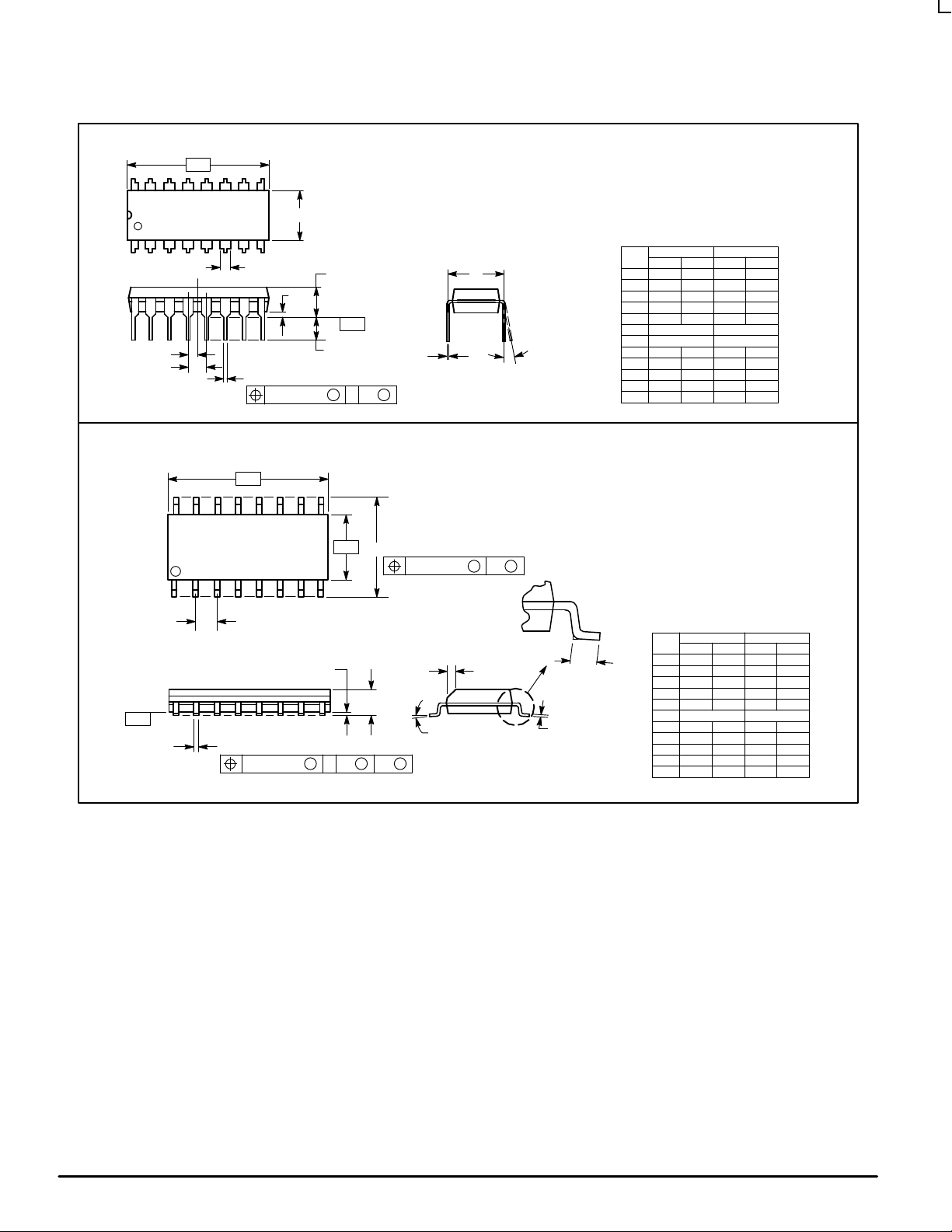
OUTLINE DIMENSIONS
N SUFFIX
–
916
B
F
C
S
SEATING
–T
PLANE
–
K
G
D
16 PL
M M
TA0.25 (0.010)
CASE 648–08
ISSUE R
L
J
M
D SUFFIX
PLASTIC SOIC PACKAGE
PLASTIC PACKAGE
P 8 PL
0.25 (0.010) B
CASE 751B–05
ISSUE J
M M
R X 45°
M
J
–A
–
G
D 16 PL
0.25 (0.010) T B A
916
–B
–
8
K
C
M
S S
NOTES:
1. DIMENSIONING AND TOLERANCING PER ANSI
Y14.5M, 1982.
2. CONTROLLING DIMENSION: INCH.
3. DIMENSION L TO CENTER OF LEADS WHEN
FORMED PARALLEL.
4. DIMENSION B DOES NOT INCLUDE MOLD FLASH.
5. ROUNDED CORNERS OPTIONAL.
INCHES MILLIMETERS
MIN MINMAX MAX
DIM
A
0.740
B
0.250
C
0.145
D
0.015
F
0.040
G
H
J
0.008
K
0.110
L
0.295
M
0
°
S
0.020
NOTES:
1. DIMENSIONING AND TOLERANCING PER ANSI
Y14.5M, 1982.
2. CONTROLLING DIMENSION: MILLIMETER.
3. DIMENSIONS A AND B DO NOT INCLUDE
MOLD PROTRUSION.
4. MAXIMUM MOLD PROTRUSION 0.15 (0.006)
PER SIDE.
5. DIMENSION D DOES NOT INCLUDE DAMBAR
PROTRUSION. ALLOWABLE DAMBAR
PROTRUSION SHALL BE 0.127 (0.005) TOTAL
IN EXCESS OF THE D DIMENSION AT
MAXIMUM MATERIAL CONDITION.
DIM
F
A
B
C
D
F
G
J
K
M
P
R
18.80
6.35
3.69
0.39
1.02
0.21
2.80
7.50
0.51
10.00
4.00
1.75
0.49
1.25
0.25
0.25
7
6.20
0.50
2.54 BSC
1.27 BSC
0
°
°
19.55
6.85
4.44
0.53
1.77
0.38
3.30
7.74
10
1.01
0.386
0.150
0.054
0.014
0.016
0.008
0.004
0
0.229
0.010
0.770
0.270
0.175
0.021
0.070
0.100 BSC
0.050 BSC
0.015
0.130
0.305
10
°
0.040
MILLIMETERS INCHES
MIN MINMAX MAX
9.80
3.80
1.35
0.35
0.40
1.27 BSC 0.050 BSC
0.19
0.10
0
°
5.80
0.25
°
°
0.393
0.157
0.068
0.019
0.049
0.009
0.009
7
0.244
0.019
°
MOTOROLA High–Speed CMOS Logic Data
8
DL129 — Rev 6

ÇÇ
0.10 (0.004)
SEATING
–T–
PLANE
L
U0.15 (0.006) T
PIN 1
IDENT.
U0.15 (0.006) T
D
S
2X L/2
S
MC74HC165A
OUTLINE DIMENSIONS
DT SUFFIX
PLASTIC TSSOP PACKAGE
CASE 948F–01
ISSUE O
16X REFK
0.10 (0.004) V
16
1
M
A
–V–
C
G
S
H
N
S
J
N
DETAIL E
DETAIL E
J1
0.25 (0.010)
F
K
K1
SECTION N–N
M
NOTES:
1. DIMENSIONING AND TOLERANCING PER ANSI
Y14.5M, 1982.
2. CONTROLLING DIMENSION: MILLIMETER.
3. DIMENSION A DOES NOT INCLUDE MOLD FLASH.
PROTRUSIONS OR GATE BURRS. MOLD FLASH OR
GATE BURRS SHALL NOT EXCEED 0.15 (0.006) PER
SIDE.
4. DIMENSION B DOES NOT INCLUDE INTERLEAD
FLASH OR PROTRUSION. INTERLEAD FLASH OR
PROTRUSION SHALL NOT EXCEED
0.25 (0.010) PER SIDE.
5. DIMENSION K DOES NOT INCLUDE DAMBAR
PROTRUSION. ALLOWABLE DAMBAR PROTRUSION
SHALL BE 0.08 (0.003) TOTAL IN EXCESS OF THE K
DIMENSION AT MAXIMUM MATERIAL CONDITION.
6. TERMINAL NUMBERS ARE SHOWN FOR
REFERENCE ONLY.
7. DIMENSION A AND B ARE TO BE DETERMINED AT
DATUM PLANE –W–.
INCHESMILLIMETERS
–W–
DIM MIN MAX MIN MAX
A 4.90 5.10 0.193 0.200
B 4.30 4.50 0.169 0.177
C ––– 1.20 ––– 0.047
D 0.05 0.15 0.002 0.006
F 0.50 0.75 0.020 0.030
G 0.65 BSC 0.026 BSC
H 0.18 0.28 0.007 0.011
J 0.09 0.20 0.004 0.008
J1 0.09 0.16 0.004 0.006
K 0.19 0.30 0.007 0.012
K1 0.19 0.25 0.007 0.010
L 6.40 BSC 0.252 BSC
M 0 8 0 8
____
U
T
9
B
–U–
8
Motorola reserves the right to make changes without further notice to any products herein. Motorola makes no warranty , representation or guarantee regarding
the suitability of its products for any particular purpose, nor does Motorola assume any liability arising out of the application or use of any product or circuit, and
specifically disclaims any and all liability, including without limitation consequential or incidental damages. “T ypical” parameters which may be provided in Motorola
data sheets and/or specifications can and do vary in different applications and actual performance may vary over time. All operating parameters, including “Typicals”
must be validated for each customer application by customer’s technical experts. Motorola does not convey any license under its patent rights nor the rights of
others. Motorola products are not designed, intended, or authorized for use as components in systems intended for surgical implant into the body, or other
applications intended to support or sustain life, or for any other application in which the failure of the Motorola product could create a situation where personal injury
or death may occur. Should Buyer purchase or use Motorola products for any such unintended or unauthorized application, Buyer shall indemnify and hold Motorola
and its officers, employees, subsidiaries, affiliates, and distributors harmless against all claims, costs, damages, and expenses, and reasonable attorney fees
arising out of, directly or indirectly, any claim of personal injury or death associated with such unintended or unauthorized use, even if such claim alleges that
Motorola was negligent regarding the design or manufacture of the part. Motorola and are registered trademarks of Motorola, Inc. Motorola, Inc. is an Equal
Opportunity/Affirmative Action Employer.
Mfax is a trademark of Motorola, Inc.
How to reach us:
USA/EUROPE /Locations Not Listed: Motorola Literature Distribution; JAPAN: Nippon Motorola Ltd.: SPD, Strategic Planning Office, 141,
P.O. Box 5405, Denver, Colorado 80217. 1–303–675–2140 or 1–800–441–2447 4–32–1 Nishi–Gotanda, Shagawa–ku, Tokyo, Japan. 03–5487–8488
Customer Focus Center: 1–800–521–6274
Mfax: RMFAX0@email.sps.mot.com – TOUCHTONE 1–602–244–6609 ASIA/PACIFIC: Motorola Semiconductors H.K. Ltd.; 8B T a i Ping Industrial Park,
Moto rola Fax Back System – US & Canada ONLY 1–800–774–1848 51 Ting Kok Road, Tai Po, N.T., Hong Kong. 852–26629298
– http://sps.motorola.com/mfax/
HOME PAGE: http://motorola.com/sps/
High–Speed CMOS Logic Data
◊
9 MOTOROLA
MC74HC165A/D
DL129 — Rev 6
 Loading...