

Motorola MC74HC165ADT, MC74HC165AD Datasheet
SEMICONDUCTOR TECHNICAL DATA
" #"
#"#" " !"
High–Performance Silicon–Gate CMOS
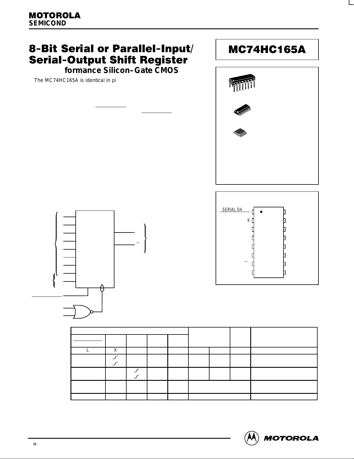
The MC74HC165A is identical in pinout to the LS165. The device inputs
are compatible with standard CMOS outputs; with pullup resistors, they are
compatible with LSTTL outputs.
This device is an 8–bit shift register with complementary outputs from the
last stage. Data may be loaded into the register either in parallel or in serial
form. When the Serial Shift/Parallel Load
asynchronously in parallel. When the Serial Shift/Parallel Load
the data is loaded serially on the rising edge of either Clock or Clock Inhibit
(see the Function Table).
The 2–input NOR clock may be used either by combining two independent
clock sources or by designating one of the clock inputs to act as a clock
inhibit.
• Output Drive Capability: 10 LSTTL Loads
• Outputs Directly Interface to CMOS, NMOS, and TTL
• Operating Voltage Range: 2 to 6 V
• Low Input Current: 1 µA
• High Noise Immunity Characteristic of CMOS Devices
• In Compliance with the Requirements Defined by JEDEC Standard
No. 7A
• Chip Complexity: 286 FETs or 71.5 Equivalent Gates
LOGIC DIAGRAM
11
A
12
B
13
PARALLEL
DATA
INPUTS
SERIAL
DATA
INPUT
SERIAL SHIFT/
PARALLEL LOAD
CLOCK INHIBIT
C
D
E
F
G
H
S
A
CLOCK
14
3
4
5
6
10
1
2
15
Serial Shift/
Parallel Load
L X X X a … h a b h Asynchronous Parallel Load
H
H
H
H
H
H
H L L X X No Change No Clock
X = don’t care QAn – QGn = Data shifted from the preceding stage
input is low, the data is loaded
input is high,
9
Q
SERIAL
H
7
DATA
OUTPUTS
Q
H
PIN 16 = V
PIN 8 = GND
CC
FUNCTION TABLE
Inputs Internal Stages Output
Clock
Clock
Inhibit
L
L
L
L
X
H
H
X
S
A
L
H
L
H
X
X
A – H Q
X
X
X
X
X
X
H
H
16
1
16
1
16
1
ORDERING INFORMATION
MC74HCXXXAN
MC74HCXXXAD
MC74HCXXXADT
PIN ASSIGNMENT
SERIAL SHIFT/
PARALLEL LOAD
CLOCK
Q
A
L
L
Q
An
Q
An
Q
An
Q
An
No Change Inhibited Clock
Q
B
Q
Gn
Q
Gn
Q
Gn
Q
Gn
1
2
E
3
F
4
G
6
H
7
Q
H
8
GND
H
Serial Shift via Clock
Serial Shift via Clock Inhibit
N SUFFIX
PLASTIC PACKAGE
CASE 648–08
D SUFFIX
SOIC PACKAGE
CASE 751B–05
DT SUFFIX
TSSOP PACKAGE
CASE 948F–01
Plastic
SOIC
TSSOP
V
16
CC
CLOCK INHIBIT
15
D
14
C
13
B
125
A
11
S
10
A
Q
9
H
Operation
This document contains information on a product under development. Motorola reserves the right to change or
discontinue this product without notice.
3/98
Motorola, Inc. 1998
1
REV 1
MC74HC165A
Î
Î
Î
Î
Î
Î
Î
Î
Î
Î
Î
Î
Î
Î
Î
Î
Î
Î
Î
Î
Î
Î
Î
Î
Î
Î
Î
Î
Î
Î
Î
Î
Î
Î
Î
Î
Î
Î
Î
Î
Î
Î
Î
Î
Î
Î
Î
Î
Î
Î
Î
Î
Î
Î
Î
Î
Î
Î
Î
Î
Î
Î
Î
Î
Î
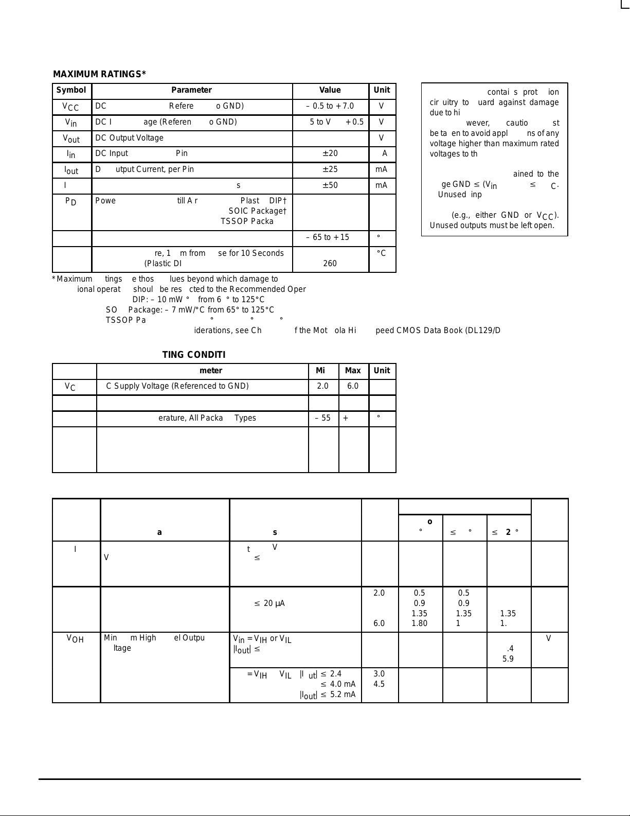
MAXIMUM RATINGS*
Symbol
V
V
I
I
Î
Î
T
Î
Î
DC Supply Voltage (Referenced to GND)
CC
V
DC Input Voltage (Referenced to GND)
in
DC Output Voltage (Referenced to GND)
out
I
DC Input Current, per Pin
in
DC Output Current, per Pin
out
DC Supply Current, VCC and GND Pins
CC
P
Power Dissipation in Still Air Plastic DIP†
D
ОООООООООООО
ОООООООООООО
Storage Temperature
stg
ОООООООООООО
T
Lead Temperature, 1 mm from Case for 10 Seconds
L
ОООООООООООО
*Maximum Ratings are those values beyond which damage to the device may occur.
Functional operation should be restricted to the Recommended Operating Conditions.
†Derating — Plastic DIP: – 10 mW/_C from 65_ to 125_C
SOIC Package: – 7 mW/_C from 65_ to 125_C
TSSOP Package: – 6.1 mW/_C from 65_ to 125_C
For high frequency or heavy load considerations, see Chapter 2 of the Motorola High–Speed CMOS Data Book (DL129/D).
Parameter
SOIC Package†
TSSOP Package†
(Plastic DIP, SOIC or TSSOP Package)
Value
– 0.5 to + 7.0
– 0.5 to VCC + 0.5
– 0.5 to VCC + 0.5
± 20
± 25
± 50
750
500
ÎÎÎÎ
450
ÎÎÎÎ
– 65 to + 150
ÎÎÎÎ
ÎÎÎÎ
260
Unit
V
V
V
mA
mA
mA
mW
Î
Î
_
C
Î
_
C
Î
This device contains protection
circuitry to guard against damage
due to high static voltages or electric
fields. However, precautions must
be taken to avoid applications of any
voltage higher than maximum rated
voltages to this high–impedance circuit. For proper operation, Vin and
V
should be constrained to the
out
range GND v (Vin or V
Unused inputs must always be
tied to an appropriate logic voltage
level (e.g., either GND or VCC).
Unused outputs must be left open.
) v VCC.
out
RECOMMENDED OPERATING CONDITIONS
Symbol
V
CC
Vin, V
T
A
tr, t
ÎÎ
ÎÎ
DC Supply Voltage (Referenced to GND)
DC Input Voltage, Output Voltage (Referenced to GND)
out
Operating Temperature, All Package Types
Input Rise and Fall Time VCC = 2.0 V
f
(Figure 1) VCC = 3.0 V
ОООООООООООО
ОООООООООООО
Parameter
VCC = 4.5 V
VCC = 6.0 V
Min
2.0
0
– 55
0
0
Î
0
Î
DC ELECTRICAL CHARACTERISTICS (Voltages Referenced to GND)
ÎÎ
Symbol
V
IH
ÎÎ
ÎÎ
V
IL
ÎÎ
ÎÎ
V
OH
ÎÎ
ÎÎÎОООООООÎООООООО
ООООООО
Parameter
Minimum High–Level Input
Voltage
ООООООО
ООООООО
Maximum Low–Level Input
Voltage
ООООООО
ООООООО
Minimum High–Level Output
Voltage
ООООООО
ООООООО
Test Conditions
V
= 0.1 V or VCC – 0.1 V
out
|I
| v 20 µA
ООООООО
out
ООООООО
V
= 0.1 V or VCC – 0.1 V
out
|I
| v 20 µA
out
ООООООО
ООООООО
Vin = VIH or V
|I
| v 20 µA
out
ООООООО
Vin = VIH or VIL|I
IL
| v 2.4 mA
out
|I
| v 4.0 mA
out
|I
| v 5.2 mA
out
Max
6.0
V
CC
+ 125
1000
600
Î
500
400
Î
Unit
V
V
_
C
ns
Î
Î
V
CC
ÎÎ
V
2.0
3.0
ÎÎ
4.5
ÎÎ
6.0
2.0
3.0
ÎÎ
4.5
ÎÎ
6.0
2.0
4.5
ÎÎ
6.0
3.0
4.5
ÎÎ
6.0
Guaranteed Limit
– 55 to
ÎÎ
25_C
ÎÎ
1.5
2.1
ÎÎ
ÎÎ
3.15
4.2
ÎÎ
ÎÎ
0.5
0.9
ÎÎ
ÎÎ
1.35
1.80
ÎÎ
ÎÎ
1.9
4.4
ÎÎ
5.9
ÎÎ
2.48
3.98
ÎÎ
ÎÎ
5.48
v
85_C
1.5
2.1
3.15
4.2
0.5
0.9
1.35
1.80
1.9
4.4
5.9
2.34
3.84
5.34
ÎÎ
v
125_C
1.5
2.1
ÎÎ
3.15
ÎÎ
4.2
0.5
0.9
ÎÎ
1.35
ÎÎ
1.80
1.9
4.4
ÎÎ
5.9
2.20
3.70
ÎÎ
5.20
Î
Unit
Î
Î
Î
Î
Î
Î
V
V
V
V
MOTOROLA High–Speed CMOS Logic Data
2
DL129 — Rev 6
MC74HC165A
Î
Î
Î
Î
Î
Î
Î
Î
Î
Î
Î
Î
Î
Î
Î
Î
Î
Î
Î
Î
Î
Î
Î
Î
Î
Î
Î
Î
Î
Î
Î
Î
Î
Î
Î
Î
Î
Î
Î
Î
Î
Î
Î
Î
Î
Î
Î
Î
Î
Î
Î
Î
Î
Î
Î
Î
Î
Î
Î
Î
Î
Î
Î
Î
Î
Î
Î
Î
Î
Î
Î
Î
Î
Î
Î
Î
Î
Î
Î
Î
Î
Î
Î
Î
Î
DC ELECTRICAL CHARACTERISTICS (Voltages Referenced to GND)
Guaranteed Limit
V
V
Symbol
Symbol
V
OL
ÎÎ
ÎÎÎОООООООÎООООООО
I
in
I
CC
ÎÎ
Maximum Low–Level Output
Voltage
ООООООО
Maximum Input Leakage Current
Maximum Quiescent Supply
ООООООО
Current (per Package)
Parameter
Parameter
Test Conditions
Test Conditions
Vin = VIH or V
|I
| v 20 µA
out
ООООООО
Vin = VIH or VIL|I
IL
| v 2.4 mA
out
|I
| v 4.0 mA
out
|I
| v 5.2 mA
out
Vin = VCC or GND
Vin = VCC or GND
ООООООО
I
= 0 µA
out
2.0
4.5
ÎÎ
6.0
3.0
4.5
ÎÎ
6.0
6.0
6.0
ÎÎ
NOTE:Information on typical parametric values can be found in Chapter 2 of the Motorola High–Speed CMOS Data Book (DL129/D).
CC
CC
V
V
– 55 to
25_C
v
0.1
0.1
ÎÎ
0.1
ÎÎ
0.26
0.26
ÎÎ
± 0.1
ÎÎ4ÎÎ
0.26
ÎÎ
± 1.0
85_C
0.1
0.1
0.1
0.33
0.33
0.33
40
v
125_C
0.1
0.1
ÎÎ
0.1
0.40
0.40
ÎÎ
0.40
± 1.0
160
ÎÎ
Unit
Unit
Î
Î
µA
µA
Î
V
AC ELECTRICAL CHARACTERISTICS (C
= 50 pF, Input tr = tf = 6 ns)
L
Guaranteed Limit
ÎÎ
Symbol
f
max
ÎÎ
ÎÎ
t
,
PLH
t
PHL
ÎÎ
ÎÎ
t
,
PLH
t
PHL
ÎÎ
ÎÎ
t
,
PLH
t
PHL
ÎÎ
ÎÎ
t
,
TLH
t
THL
ÎÎ
ÎÎ
C
in
ООООООООООООООО
Parameter
Maximum Clock Frequency (50% Duty Cycle)
(Figures 1 and 8)
ООООООООООООООО
ООООООООООООООО
Maximum Propagation Delay, Clock (or Clock Inhibit) to QH or Q
(Figures 1 and 8)
ООООООООООООООО
ООООООООООООООО
Maximum Propagation Delay, Serial Shift/Parallel Load to QH or Q
(Figures 2 and 8)
ООООООООООООООО
ООООООООООООООО
Maximum Propagation Delay, Input H to QH or Q
(Figures 3 and 8)
ООООООООООООООО
ООООООООООООООО
H
Maximum Output Transition Time, Any Output
(Figures 1 and 8)
ООООООООООООООО
ООООООООООООООО
Maximum Input Capacitance
H
H
V
CC
ÎÎ
2.0
3.0
ÎÎ
4.5
ÎÎ
6.0
2.0
3.0
ÎÎ
4.5
ÎÎ
6.0
2.0
3.0
ÎÎ
4.5
ÎÎ
6.0
2.0
3.0
ÎÎ
4.5
6.0
ÎÎ
2.0
3.0
ÎÎ
4.5
6.0
ÎÎ
—
– 55 to
V
ÎÎ
25_C
ÎÎ
ÎÎ
ÎÎ
ÎÎ
ÎÎ
ÎÎ
ÎÎ
ÎÎ
ÎÎ
ÎÎ
6
18
30
35
150
52
30
26
175
58
35
30
150
52
30
26
75
27
15
13
10
ÎÎ
v
85_C
4.8
17
ÎÎ
24
ÎÎ
28
190
63
ÎÎ
38
ÎÎ
33
220
70
ÎÎ
44
ÎÎ
37
190
63
ÎÎ
38
33
ÎÎ
95
32
ÎÎ
19
16
ÎÎ
10
ÎÎ
v
125_C
ÎÎ
ÎÎ
ÎÎ
ÎÎ
ÎÎ
ÎÎ
ÎÎ
ÎÎ
ÎÎ
ÎÎ
NOTES:
1. For propagation delays with loads other than 50 pF, see Chapter 2 of the Motorola High–Speed CMOS Data Book (DL129/D).
2. Information on typical parametric values can be found in Chapter 2 of the Motorola High–Speed CMOS Data Book (DL129/D).
4
15
20
24
225
65
45
38
265
72
53
45
225
65
45
38
110
36
22
19
10
Î
Unit
MHz
Î
Î
Î
Î
Î
Î
Î
Î
Î
Î
pF
ns
ns
ns
ns
C
PD
Power Dissipation Capacitance (Per Package)*
*Used to determine the no–load dynamic power consumption: PD = CPD V
Motorola High–Speed CMOS Data Book (DL129/D).
High–Speed CMOS Logic Data
DL129 — Rev 6
Typical @ 25°C, VCC = 5.0 V
40
2
f + ICC VCC. For load considerations, see Chapter 2 of the
CC
pF
3 MOTOROLA
 Loading...