

Motorola MC74HC164AD, MC74HC164ADT, MC54HC164AJ Datasheet
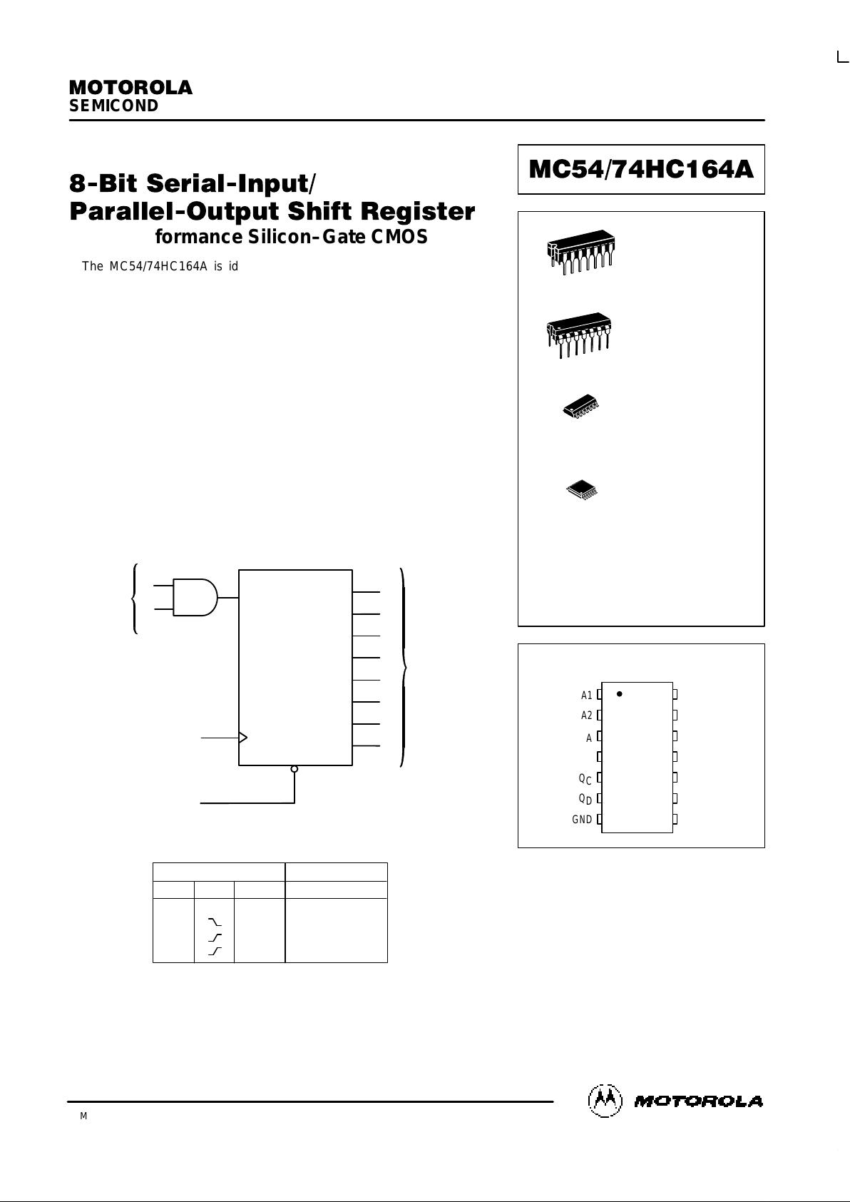
SEMICONDUCTOR TECHNICAL DATA
3–1
REV 0
Motorola, Inc. 1996
3/96
! "!
"!"! ! !
High–Performance Silicon–Gate CMOS
The MC54/74HC164A is identical in pinout to the LS164. The device
inputs are compatible with standard CMOS outputs; with pullup resistors,
they are compatible with LSTTL outputs.
The MC54/74HC164A is an 8–bit, serial–input to p arallel–output s hift
register. Two serial data inputs, A1 and A2, are provided so that one input
may be used as a data enable. Data is entered on each rising edge of the
clock. The active–low asynchronous Reset overrides the Clock and Serial
Data inputs.
• Output Drive Capability: 10 LSTTL Loads
• Outputs Directly Interface to CMOS, NMOS, and TTL
• Operating Voltage Range: 2 to 6 V
• Low Input Current: 1
µA
• High Noise Immunity Characteristic of CMOS Devices
• In Compliance with the Requirements Defined by JEDEC Standard
No. 7A
• Chip Complexity: 244 FETs or 61 Equivalent Gates
LOGIC DIAGRAM
PIN 14 = V
CC
PIN 7 = GND
3
Q
A
4
5
6
10
11
12
13
Q
B
Q
C
Q
D
Q
E
Q
F
Q
G
Q
H
PARALLEL
DATA
OUTPUTS
9
RESET
CLOCK
8
SERIAL
DATA
INPUTS
A1
A2
1
2
DATA
FUNCTION TABLE
Inputs Outputs
Reset Clock A1 A2 QAQB… Q
H
L X X X L L … L
H X X No Change
H H D D QAn… Q
Gn
H D H D QAn… Q
Gn
D = data input
QAn – QGn = data shifted from the preceding
stage on a rising edge at the clock input.
D SUFFIX
SOIC PACKAGE
CASE 751A–03
N SUFFIX
PLASTIC PACKAGE
CASE 646–06
ORDERING INFORMATION
MC54HCXXXAJ
MC74HCXXXAN
MC74HCXXXAD
MC74HCXXXADT
Ceramic
Plastic
SOIC
TSSOP
1
14
1
14
1
14
DT SUFFIX
TSSOP PACKAGE
CASE 948G–01
J SUFFIX
CERAMIC PACKAGE
CASE 632–08
1
14
PIN ASSIGNMENT
11
12
13
14
8
9
105
4
3
2
1
7
6
Q
E
Q
F
Q
G
Q
H
V
CC
CLOCK
RESET
Q
B
Q
A
A2
A1
GND
Q
D
Q
C
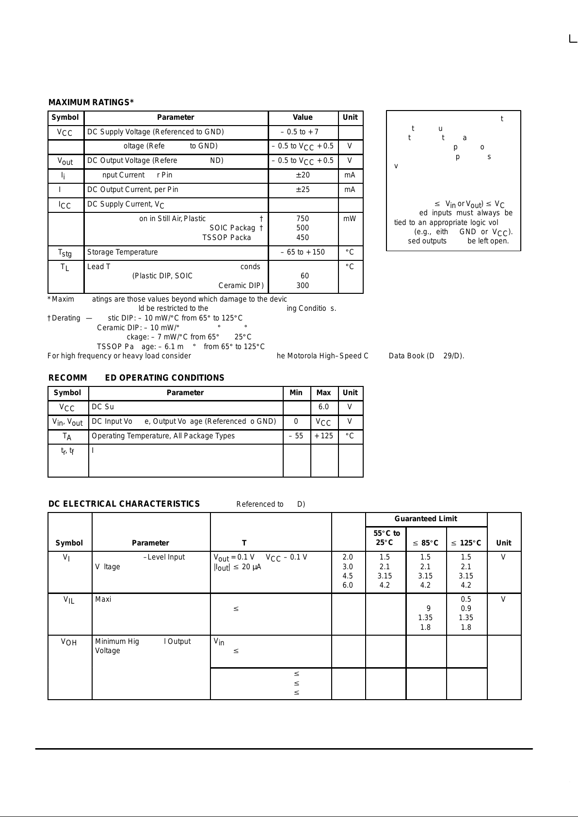
MC54/74HC164A
MOTOROLA High–Speed CMOS Logic Data
DL129 — Rev 6
3–2
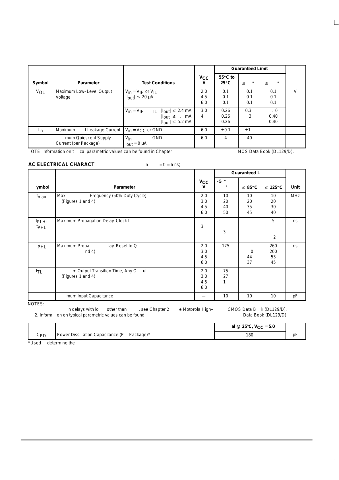
MAXIMUM RATINGS*
Symbol
Parameter
Value
Unit
V
CC
DC Supply Voltage (Referenced to GND)
– 0.5 to + 7.0
V
V
in
DC Input Voltage (Referenced to GND)
– 0.5 to VCC + 0.5
V
V
out
DC Output Voltage (Referenced to GND)
– 0.5 to VCC + 0.5
V
I
in
DC Input Current, per Pin
± 20
mA
I
out
DC Output Current, per Pin
± 25
mA
I
CC
DC Supply Current, VCC and GND Pins
± 50
mA
P
D
Power Dissipation in Still Air,Plastic or Ceramic DIP†
SOIC Package†
TSSOP Package†
750
500
450
mW
T
stg
Storage Temperature
– 65 to + 150
_
C
T
L
Lead Temperature, 1 mm from Case for 10 Seconds
(Plastic DIP, SOIC or TSSOP Package)
(Ceramic DIP)
260
300
_
C
*Maximum Ratings are those values beyond which damage to the device may occur.
Functional operation should be restricted to the Recommended Operating Conditions.
†Derating — Plastic DIP: – 10 mW/_C from 65_ to 125_C
Ceramic DIP: – 10 mW/_C from 100_ to 125_C
SOIC Package: – 7 mW/_C from 65_ to 125_C
TSSOP Package: – 6.1 mW/_C from 65_ to 125_C
For high frequency or heavy load considerations, see Chapter 2 of the Motorola High–Speed CMOS Data Book (DL129/D).
RECOMMENDED OPERATING CONDITIONS
Symbol
Parameter
Min
Max
Unit
V
CC
DC Supply Voltage (Referenced to GND)
2.0
6.0
V
Vin, V
out
DC Input Voltage, Output Voltage (Referenced to GND)
0
V
CC
V
T
A
Operating Temperature, All Package Types
– 55
+ 125
_
C
tr, t
f
Input Rise and Fall Time VCC = 2.0 V
(Figure 1) VCC = 4.5 V
VCC = 6.0 V
0
0
0
1000
500
400
ns
DC ELECTRICAL CHARACTERISTICS (Voltages Referenced to GND)
Guaranteed Limit
Symbol
Parameter
Test Conditions
V
CC
V
–55_C to
25_C
v
85_Cv 125_C
Unit
V
IH
Minimum High–Level Input
Voltage
V
out
= 0.1 V or VCC – 0.1 V
|I
out
| v 20 µA
2.0
3.0
4.5
6.0
1.5
2.1
3.15
4.2
1.5
2.1
3.15
4.2
1.5
2.1
3.15
4.2
V
V
IL
Maximum Low–Level Input
Voltage
V
out
= 0.1 V or VCC – 0.1 V
|I
out
| v 20 µA
2.0
3.0
4.5
6.0
0.5
0.9
1.35
1.8
0.5
0.9
1.35
1.8
0.5
0.9
1.35
1.8
V
V
OH
Minimum High–Level Output
Voltage
Vin = VIH or V
IL
|I
out
| v 20 µA
2.0
4.5
6.0
1.9
4.4
5.9
1.9
4.4
5.9
1.9
4.4
5.9
V
Vin = VIH or VIL|I
out
| v 2.4 mA
|I
out
| v 4.0 mA
|I
out
| v 5.2 mA
3.0
4.5
6.0
2.48
3.98
5.48
2.34
3.84
5.34
2.20
3.70
5.20
This device contains protection
circuitry to guard against damage
due to high static voltages or electric
fields. However, precautions must
be taken to avoid applications of any
voltage higher than maximum rated
voltages to this high–impedance circuit. For proper operation, Vin and
V
out
should be constrained to the
range GND v (Vin or V
out
) v VCC.
Unused inputs must always be
tied to an appropriate logic voltage
level (e.g., either GND or VCC).
Unused outputs must be left open.
MC54/74HC164A
High–Speed CMOS Logic Data
DL129 — Rev 6
3–3 MOTOROLA
DC ELECTRICAL CHARACTERISTICS (Voltages Referenced to GND)
Unit
Guaranteed Limit
V
CC
V
Test Conditions
Parameter
Symbol
Unit
v
125_C
v
85_C
–55_C to
25_C
V
CC
V
Test Conditions
Parameter
Symbol
V
OL
Maximum Low–Level Output
Voltage
Vin = VIH or V
IL
|I
out
| v 20 µA
2.0
4.5
6.0
0.1
0.1
0.1
0.1
0.1
0.1
0.1
0.1
0.1
V
Vin = VIH or VIL|I
out
| v 2.4 mA
|I
out
| v 4.0 mA
|I
out
| v 5.2 mA
3.0
4.5
6.0
0.26
0.26
0.26
0.33
0.33
0.33
0.40
0.40
0.40
I
in
Maximum Input Leakage Current
Vin = VCC or GND
6.0
± 0.1
± 1.0
± 1.0
µA
I
CC
Maximum Quiescent Supply
Current (per Package)
Vin = VCC or GND
I
out
= 0 µA
6.0
4
40
160
µA
NOTE: Information on typical parametric values can be found in Chapter 2 of the Motorola High–Speed CMOS Data Book (DL129/D).
AC ELECTRICAL CHARACTERISTICS (C
L
= 50 pF, Input tr = tf = 6 ns)
Guaranteed Limit
Symbol
Parameter
V
CC
V
–55_C to
25_C
v
85_Cv 125_C
Unit
f
max
Maximum Clock Frequency (50% Duty Cycle)
(Figures 1 and 4)
2.0
3.0
4.5
6.0
10
20
40
50
10
20
35
45
10
20
30
40
MHz
t
PLH
,
t
PHL
Maximum Propagation Delay, Clock to Q
(Figures 1 and 4)
2.0
3.0
4.5
6.0
160
100
32
27
200
150
40
34
250
200
48
42
ns
t
PHL
Maximum Propagation Delay, Reset to Q
(Figures 2 and 4)
2.0
3.0
4.5
6.0
175
100
35
30
220
150
44
37
260
200
53
45
ns
t
TLH
,
t
THL
Maximum Output Transition Time, Any Output
(Figures 1 and 4)
2.0
3.0
4.5
6.0
75
27
15
13
95
32
19
16
110
36
22
19
ns
C
in
Maximum Input Capacitance
—
10
10
10
pF
NOTES:
1. For propagation delays with loads other than 50 pF, see Chapter 2 of the Motorola High–Speed CMOS Data Book (DL129/D).
2. Information on typical parametric values can be found in Chapter 2 of the Motorola High–Speed CMOS Data Book (DL129/D).
Typical @ 25°C, VCC = 5.0 V
C
PD
Power Dissipation Capacitance (Per Package)*
180
pF
*Used to determine the no–load dynamic power consumption: PD = CPD V
CC
2
f + ICC VCC. For load considerations, see Chapter 2 of the
Motorola High–Speed CMOS Data Book (DL129/D).
 Loading...